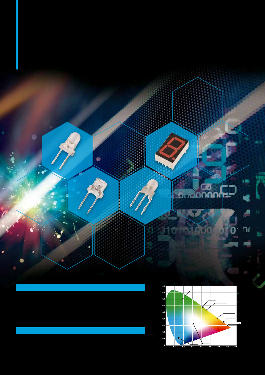
background image

— 95 —

— 95 —

Through-hole LED

Numeric Display

縦型LED/Through-hole LED

数字表示/LED numeric display

縦型LED/Through-hole LED

数字表示/LED numeric display

NAR131SH-F,NAR141SH-F,NAR161H-F,
NAG131SPH-F

NAG161PH-F

CIE1931 Chromaticity Diagram

(y)

(x)

THG

YPY,F□D

FR,F□R,VR

FY,F□Y

FA,F□A

FR,F□R,VR

THW

THB

PG

φ3タイプ/φ3Type LED

3801C,3863X,3

64X,3809X

φ3 2色発光タイプ/Bi- Color Type LED

3312X

1610catalog02-html.html
background image

— 96 —

縦型LEDランプ/THROUGH-HOLE LED

φ

3

FA 

FR 

603 

590 

605

626

624

624


FA

FR 

PG 

F□D

F□R

YPY

F□A

F□D

YPY

F□A

F□R

FY

FY

VR

VR

F□Y 

THW


THB 

470 

THG 

525  567  572  572  588

THW  THB  THG  PG 

F□Y

3 8 6 3 X

3 □ 6 4

X

3 8 0 9 X

3 3 1 2 X

3 8 0 1 C

     ドミナント波長
Dominant Wavelength

丸形2色

Bi-colo

r

R

ound 

S

hape

Type


スペクトル分布/

SPECTRAL 

D

ISTRIBUTION

白 色/White

THW

青 色/Blue

THB

緑 色/Green

THG, PG

黄緑色/Yellow Green

YPY, F□D

黄 色/Yellow

FY, F□Y

橙 色/Orange

FA, F□A

赤 色/Red

VR, FR,

F□R

THW

THB

THG

YPY

F□D

F□

Y

  FY

F□

R

400 

450 

500 

550 

600 

650 

700 

750 

800

波長/ Wavelength λ (nm)

相対放射強度

Relative Intentsity

FR

0.5

0

1.0

P G

  VR


F□

A

FA

セレクションガイド/SELECTION GUIDE

1610catalog02-html.html
background image

— 97 —

発光素子/

LED Die Material

材質/

Material

発光色/

Emitted Color

InGaN

AlGaInP

白色/

White

THW

青色/

Blue

THB

緑色/

Green

THG

黄緑色/

Yellow Green

YPY/F

D

黄色/

Yellow

FY/F

Y

橙色/

Orange

FA/F□A

赤色/

Red

FR/F□R

外形寸法/

Package Size


3

3.1m

m  

リードフレーム/

LED Construction


8,C

0.4mm

反射鏡付長リード/

0.4mm square lead with reflector

レンズカラー/

Lens Color


0

=無色透明/

Water clear


6

=淡着色透明/

Pale color clear

形状追番/

Additional Number of Shape

外観形状/

Outer Shape Suffix


C, X

=丸形/

Roun

d  

F R 3 8 6 3 X


VR PG 3312 X


発光素子/

LED Die Material

材質/

Material

発光色/

Emitted Color

G a P

G a A s P

緑色/

Green

P G

赤色/

Red

V R

外形寸法/

Package Size


3

3.1mm 

リードフレーム/

LED Construction


3

=φ 3 用 3 本足リード/φ

3 with three lead

レンズカラー/

Lens  Color


1

=乳白色拡散/

White diffused

形状追番/

Additional Number of Shape

外観形状/

Outer Shape Suffix


X

=丸形/

Round

テーピングご注意

縦型

LED

のテーピング品をご検討の際には、弊社営業窓口または特約店へご確認 下さい。

Taping precautions

If taped through-hole LEDs are needed, please confirm with our sales or agents. 

縦型

LED

ランプ/

THROUGH-HOLE LED

2

色発光縦型

LED

ランプ/

BI-COLOR THROUGH-HOLE LED

品名表示方法/DESCRIPTION OF PART NUMBER

1610catalog02-html.html
background image

— 98 —

SINGLE-COLOR LED

For further information, please refer to this WEB site.

http://www.stanley-components.com/en/product/vertical.html

φ

3mm TYPE


丸形直付けタイプ/Direct mount round shape type  

0.6MAX.

0.4±0.1

(2.5)

(1)

φ4.2±0.2

φ3.1±0.1

2.9±0.2

6.6±0.3

31MIN.

29MIN.

(2.3)

0.5MAX.

φ4.2±0.1

φ3.1±0.1

(2.5)

2.2±0.2

0.5MAX.

(1.7)

30MIN.

28MIN.

0.6MAX.

0.4±0.1

5.9±0.3

C0.55

(1)

fig.1 

fig.2

外観図/Package dimensions

〈unit:mm〉

発光色別定格・特性/Characteristics 

b

y co

l

or


T

a

=

25℃

品 名

Part No.

材 質

Material

発光色

Emitted Color

絶対最大定格/Absolute Maximum Ratings

電気的光学的特性/Electro-Optical Characteristics

許容損失

Power

Dissipation

Pd

順電流

Continuous

Forward

Current

I

F

パルス順電流

Repetitive

Peak 

Forward

Current 

I

FRM

逆電圧

Reverse

Voltage

V

R

動作温度
Operating

Temperature

Topr

保存温度

Storage

Temperature

Tstg

順電流 
低減率 

Derating

※2

※1

Δ

I

順電圧

Forward Voltage

V

F

逆電流

Reverse Current

I

R

色度座標

Chromaticity Coordinates

x   y    

TYP.

MAX.

I

F

MAX.

V

R

TYP.

TYP.

I

F

THW

InGaN

White

36

10

20

5

-40〜+85 -40〜+100 0.13

2.9

3.3

5

100

5

0.31

0.32

5

単位/Unit

mW

mA

mA

V

mA/℃

V

mA

μA

V

mA


T

a

=

25℃

形 状

Shape

品 名

Part No.

発光色

Emitted Color

レンズ

Lens Color

発光光度 

Luminous Intensity

Iv (mcd)

指向特性

(形状の代表例を掲載しています)

S

patial Distri

b

ution 

E

xamp

l

e

T

he typical distri

b

ution examp

l

e o

f

each shape is shown 

b

e

l

ow.


f

ig

.

MIN.

TYP.

I

F

(mA)

1

THW3801C

White

Water Clear

800

1,600

5

90° 

60° 

30° 

0° 

30° 

60° 

90° 

0.5

2

THW3809X

White

Water Clear

100

200

5

90° 

60° 

30° 

0° 

30° 

60° 

90° 

0.5

※ 1 I

FRM

の条件は

t

w ≦ 1ms  Duty ≦ 1/20 

※ 1 I

FRM

 condition : tw ≦ 1ms and duty cycle ≦ 1/20

※ 2 Ta = 25℃以上の電流低減率 

※ 2 The current derating for operation applies when the temperature is above 25℃

高輝度/High-brightness LED 

NEW

NEW

(質量/Weight:160mg)

(質量/Weight:160mg)

1610catalog02-html.html
background image

— 99 —

For further information, please refer to this WEB site.

http://www.stanley-components.com/en/product/vertical.html

SINGLE-COLOR LED

φ

3mm TYPE

丸形直付けタイプ/Direct mount round shape type 

発光色別定格・特性/Characteristics 

b

y co

l

or

Ta= 25

品 名

Part No.

材 質

Material

発光色

Emitted Color

絶対最大定格/Absolute Maximum Ratings

電気的光学的特性/Electro-Optical Characteristics

許容損失

Power

Dissipation

Pd

順電流

Continuous

Forward

Current

I

F

パルス順電流

Reprtiti

v

e

Peak 

Forward

Current 

I

FRM

逆電圧

Reverse

Voltage

V

R

動作温度
Operating

Temperature

Topr

保存温度

Storage

Temperature

Tstg

順電流 
低減率 

Derating

※2

※1

Δ

I

順電圧

Forward Voltage

V

F

逆電流

Reverse Current

I

R

発光波長/Wavelength

ドミナント
Dominant


λd

TYP

.

ピーク 

P

eak

λp

TYP

.

半値幅

S

pectral 

L

in e


H

a

l

f Width

Δ

λ

TYP

.

TYP.

MAX.

I

F

MAX.

V

R

I

F

InGaN

Blue

38

10

20

5

-40〜+85 -40〜+100

0.13

3.0

3.5

5

100

5

470

465

25

5

InGaN

Green

38

10

20

5

-40〜+85 -40〜+100

0.13

3.0

3.5

5

100

5

530

520

35  

5

単位/Unit

mW

mA

mA

V

mA/℃

V

mA

μA

V

nm

mA

Ta= 25

形 状

Shape

品 名

Part No.

発光色

Emitted Color

レンズ

Lens Color

ピーク発光波長

P

eak

Wa

v

e

l

ength

発光光度 

L

um i nous 

I

ntensity

I

(

m c d

)

指向特性

(形状の代表例を掲載しています)

S

pati al D i stri

b

u ti o n 

E

xam p

l

e

T

h e typi ca l di stri

b

u ti o n exam p

l

e o

f

eac h sh ap e i s sh o wn 

b

e

l

o w.


fig.

λp 

(

n m

)

MIN.

TYP.

I

F

(mA)

(質量/Weight:160mg)

Blue

Water Clear

465

600

1,200

5

3

Green

520

1,400 3,500

5


1 I

FRM

の条件はt

w

≦1ms  Dut

y

≦1/20 

1 I

FRM

 condition : t

w

≦1ms and duty cycl

e

≦1/20

2 Ta

=25℃以上の電流低減率 

※ 2 The current derating for operation applies when the temperature is above 25℃

超高輝度/Ultra High-brightness LED


高輝度/High-brightness LED


Ta= 25

形 状

Shape

品 名

Part No.

発光色

Emitted Color

レンズ

Lens Color

ピーク発光波長

P

eak

Wa

v

e

l

ength

発光光度 

L

um i nous 

I

ntensity

I

(

m c d

)

指向特性

(形状の代表例を掲載しています)

S

pati al D i stri

b

u ti o n 

E

xam p

l

e

T

h e typi ca l di stri

b

u ti o n exam p

l

e o

f

eac h sh ap e i s sh o wn 

b

e

l

o w.


fig.

λp 

(

n m

)

MIN.

TYP.

I

F

(mA)

Blue

Water Clear

465

35

75

5

0.5

4

Green

520

90

180

5


0.6MAX.

0.4±0.1

(2.5)

(1)

φ4.2±0.2

φ3.1±0.1

2.9±0.2

6.6±0.3

31MIN.

29MIN.

(2.3)

0.5MAX.

外観図/Package dimensions

fig.

3

φ4.2±0.1

φ3.1±0.1

(2.5)

2.2±0.2

0.5MAX.

(1.7)

30MIN.

28MIN.

0.6MAX.

0.4±0.1

5.9±0.3

C0.55

(1)

〈unit:mm〉

fig.

4

THB

THG

THB3801C

THG3801C

THB3809X

THG3809X

NEW

NEW

NEW

NEW

0.5

(質量/Weight:160mg)

1610catalog02-html.html
background image

— 100 —

SINGLE-COLOR LED

For further information, please refer to this WEB site.

http://www.stanley-components.com/en/product/vertical.html

φ

3mm TYPE


丸形直付けタイプ/Direct mount round shape type  

発光色別定格・特性/Characteristics 

b

y co

l

or


Ta=25

AlGaInP

Yellow 

Red 

125

50

100

5

-40〜+85 -40〜+100

0.67

2.3

2.5

20

100

5

590

592

20

20

AlGaInP

125

50

100

5

-40〜+85 -40〜+100

0.67

2.2

2.5

20

100

5

625

635

20

20

品 名

Part No.

材 質

Material

発光色

Emitted Color

絶対最大定格/Absolute Maximum Ratings

電気的光学的特性/Electro-Optical Characteristics

許容損失

Power

Dissipation

Pd

順電流

Continuous

Forward

Current

I

F

パルス順電流

Reprtiti

v

e

Peak 

Forward

Current 

I

FRM

逆電圧

Reverse

Voltage

V

R

動作温度
Operating

Temperature

Topr

保存温度

Storage

Temperature

Tstg

順電流 
低減率 

Derating

※2

※1

Δ

I

順電圧

Forward Voltage

V

F

逆電流

Reverse Current

I

R

発光波長/Wavelength

ドミナント
Dominant 

λd

TYP

.

ピーク 

P

eak

λp

TYP

.

半値幅


S

pectral 

L

in e


H

a

l

f Width

Δ

λ

TYP

.

TYP.

MAX.

I

F

MAX.

V

R

I

F

Yellow Green

Yellow 

130

50

200

5

-40〜+85 -40〜+100

0.67

2.1

2.5

20

100

5

572

575

15

20

AlGaInP

AlGaInP
AlGaInP

Red

Ta= 25

形 状

Shape

品 名

Part No.

発光色

Emitted Color

レンズ

Lens Color

ピーク発光波長

P

eak

Wa

v

e

l

ength

発光光度 

L

um i nous 

I

ntensity

I

(

m c d

)

指向特性

(形状の代表例を掲載しています)

S

pati al D i stri

b

u ti o n 

E

xam p

l

e

T

h e typi ca l di stri

b

u ti o n exam p

l

e o

f

eac h sh ap e i s sh o wn 

b

e

l

o w.


fig.

λp 

(

n m

)

MIN.

TYP.

I

F

(mA)

Yellow Green

Pale Yellow

575

592

180

360

20

20

Orange

Pale Orange

609

400

360

800

720

20

Red

Pale Red

635

320

640

20

Pale Yellow

Clear

Yellow

125

20

200

5

-40〜+85 -40〜+100

0.67

1.9

2.4

20

100

5

590

592

15

50

5

1.9

2.4

100

626

635

15

1

AlGaInP

Orange

125
125

50

200
200

5

-40〜+85
-40〜+85

-40〜+100
-40〜+100

0.67
0.67

1.9

2.4

20
20

100

5
5

605

609

15

20

20

20

単位/Unit

mW

mA

mA

V

mA/℃

V

mA

μA

V

nm

mA

高輝度/High-brightness LED 

1


 I

FRM

の条件は

tw

1ms  Duty

1/20 

1 I

FRM

 condition : tw

1ms and duty cycle

1/20

2 Ta

= 25℃以上の電流低減率 

2 The current derating for operation applies when the temperatu

re is above 25℃


Ta= 25

形 状

Shape

品 名

Part No.

発光色

Emitted Color

レンズ

Lens Color

ピーク発光波長

P

eak

Wa

v

e

l

ength

発光光度 

L

um i nous 

I

ntensity

I

(

m c d

)

指向特性

(形状の代表例を掲載しています)

S

pati al D i stri

b

u ti o n 

E

xam p

l

e

T

h e typi ca l di stri

b

u ti o n exam p

l

e o

f

eac h sh ap e i s sh o wn 

b

e

l

o w.


fig.

λp 

(

n m

)

MIN.

TYP.

I

F

(mA)

Yellow 

Clear

Pale Yellow

Pale Red

1

Red

635

592

1,400

1,400

2,800

2,800

20

20

超高輝度/Ultra High-brightness LED 

0.5

〈unit:mm〉

外観図/Package dimensions

φ4.2±0.1

φ3.1±0.1

(2.5)

4±0.2

0.5MAX.

(1.7)

30MIN.

28MIN.

0.6MAX.

0.4±0.1

5.9±0.3

C0.55

(1)

fig. 1

FKY3863X

FKR3863X

YPY3863X

FA3863X

FY3863X

FR3863X

FKY

FKR
YPY

FA

FR

FY

0.5

(質量

/Weight

:160mg)

(質量

/Weight

:160mg)

1610catalog02-html.html
background image

— 101 —

For further information, please refer to this WEB site.

http://www.stanley-components.com/en/product/vertical.html

SINGLE-COLOR LED

φ

3mm TYPE

丸形直付けタイプ、ブローホール対策品

/Direct mount round shape type,  Blowhole-free structure

※ 


(5.5)

(1)

(0.92)

1.7

±0.1

(2.5)

31MIN.

29MIN.

6.5

±0.3

□0.4±

0.1

0.6MAX.

(2.3)

2.9±

0.2

φ3.1±0.1

φ4.2±0.2

fig.

2


〈unit:mm〉

外観図/Package dimensions

Orange

T

a

= 25

品 名

Part No.

材 質

Material

発光色

Emitted Color

絶対最大定格/Absolute Maximum Ratings

電気的光学的特性/Electro-Optical Characteristics

許容損失

Power

Dissipation

Pd

順電流

Continuous

Forward

Current

I

F

パルス順電流

Reprtiti

v

e

Peak 

Forward

Current 

I

FRM

逆電圧

Reverse

Voltage

V

R

動作温度
Operating

Temperature

Topr

保存温度

Storage

Temperature

Tstg

順電流 
低減率 

Derating

※2

※1

Δ

I

順電圧

Forward Voltage

V

F

逆電流

Reverse Current

I

R

発光波長/Wavelength

ドミナント
Dominant  

λd

TYP

.

ピーク 

P

eak

λp

TYP

.

半値幅


S

pectral 

L

in e


H

alf Width

Δ

λ

TYP

.

TYP.

MAX.

I

F

MAX.

V

R

I

F

AlGaInP

Yellow Green

Yellow 

50

20

60

4

-30〜+85 -30〜+100

0.27

1.9

2.5

10

100

4

572

575

15

10

AlGaInP

AlGaInP

T

a

= 25

Yellow Green

Pale Yellow

Clear

575

35

100

10

Yellow

592

125

350

10

Orange

Pale Orange

608

125

350

10

Red

Pale Red

635

55

160

10

50

20

60

4

-30〜+85 -30〜+100

0.27

1.9

2.5

10

100

4

588

592

15

10

50

20

60

4

-30〜+85 -30〜+100

0.27

1.9

2.5

10

100

4

603

608

15

10

AlGaInP

Red

単位/Unit

mW

mA

mA

V

mA/℃

V

mA

μA

V

nm

mA

50

20

60

4

-30〜+85 -30〜+100

0.27

1.9

2.4

10

100

4

624

635

15

10

ブローホール対策品

 ブローホールとは、直付けタイプLEDに多く発生することがあり、はんだ付けの加熱の際に吸湿した基板などの水分が気化しはんだに穴を生じさせます。
 当製品はブローホールの発生を抑制した新構造を採用しています。

Blowhole-free structure


Bl

owho

l

e is a type of defect w

h

ich mos

t

ly


occu

r

s


in


direc

t m

oun

t

ing 

LED.

Mois

t

ure


absorbed by PCB du

r

ing so

l

de

r

ing

, m

igh

ge

t

 vaporization


andpunc

t

ure


holes in


solder

.


Bl

owho

l

e-free is a new structure w

h

ic

can p

r

even

t t

he occur

r

ence


of


blowho

l

e

.

1


 I

FRM

の条件は

t

w ≦ 1ms  Duty ≦

1/20 

1 I

FRM

 condition : tw ≦ 1ms and duty cycle ≦

1/20

2 T

a = 25℃以上の電流低減率 

※ 2 The current derating for operation applies when the temperature is above 25℃

標準輝度/Standard-brightness LED

T

a

= 25

形 状

Shape

品 名

Part No.

発光色

Emitted Color

レンズ

Lens Color

ピーク発光波長

P

eak

Wa

v

elength

発光光度 

L

um i nous 

I

ntensity

I

(

m cd

)

指向特性

(形状の代表例を掲載しています)

S

pati al D i stri bu ti o n 

E

xam pl e

T

h e typi ca l di stri bu ti o n exam pl e o f

eac h sh ap e i s sh o wn bel o w.


fig

.

λp 

(

n m

)

MIN.

TYP.

I

F

(mA)

Yellow 

Pale Yellow

Clear

Pale Red

2

Red

635

592

500

500

1,000

1,000

20

20

超高輝度/Ultra High-brightness 

0.5

形 状

Shape

品 名

Part No.

発光色

Emitted Color

レンズ

Lens Color

ピーク発光波長

P

eak

Wa

v

elength

発光光度 

L

um i nous 

I

ntensity

I

(

m cd

)

指向特性

(形状の代表例を掲載しています)

S

pati al D i stri bu ti o n 

E

xam pl e

T

h e typi ca l di stri bu ti o n exam pl e o f

eac h sh ap e i s sh o wn bel o w.


fig

.

λp 

(

n m

)

MIN.

TYP.

I

F

(mA)

2

AlGaInP

Yellow 

Red 

125

50

100

5

-40〜+85 -40〜+100

0.67

2.3

2.5

20

100

5

590

592

20

20

AlGaInP

125

50

100

5

-40〜+85 -40〜+100

0.67

2.2

2.5

20

100

5

625

635

20

20

FHD
FHY
FHA
FHR

FKY
FKR

FKY3C64X-H

FKR3C64X-H

FHD3C64X-H

FHY3C64X-H

FHA3C64X-H

FHR3C64X-H

0.5

発光色別定格・特性/Characteristics by color

(質量

/

Weight:160mg)

(質量

/

Weight:160mg)

1610catalog02-html.html
background image

— 102 —

BI-COLOR LED

For further information, please refer to this WEB site.

http://www.stanley-components.com/en/product/color.html

φ

3mm TYPE


丸形直付けタイプ/Direct mount round shape type  

発光色別定格・特性/Characteristics 

b

y co

l

or

Ta= 25

形 状

Shape

品 名

Part No.

発光色

Emitted Color

レンズ

Lens Color

ピーク発光波長

P

ea

k

W

a

v

e

l

en

g

th

発光光度 

L

um i nous 

I

ntensity

I

(

m c d

)

指向特性

(形状の代表例を掲載しています)

S

pati al D i stri

b

u ti o n 

E x

am p

l

e

T

h e typi ca l di stri

b

u ti o n e

x

am p

l

e o

f

eac h sh ap e i s sh o

w

b

e

l

o

w

.


fig.

λp 

(

n m

)

MIN.

TYP.

I

F

(mA)

Milky White

 Diffused

0.5

VR

PG

1

Green

560

6

12

20

Red

630

4

8

Ta=25℃

品 名

Part No.

材 質

Material

発光色

Emitted Color

絶対最大定格/Absolute Maximum Ratings

電気的光学的特性/Electro-Optical Characteristics

許容損失

Power

Dissipation

Pd

順電流

Continuous

Forward

Current

I

F

パルス順電流

Repetiti

v

e

Pesk Forward

Current  

I

FRM

逆電圧

Reverse

Voltage

V

R

動作温度
Operating

Temperature

Topr

保存温度

Storage

Temperature

Tstg

順電流 
低減率 

Derating

※2

※1

Δ

I

順電圧

Forward Voltage

V

F

逆電流

Reverse Current

I

R

発光波長/Wavelength

ドミナント

Dominant  

λd

TYP

.

ピーク 

P

ea

k

λp

TYP

.

半値幅


S

pectral 

L

in e


H

a

l

W

idth

Δ

λ

TYP

.

TYP.

MAX.

I

F

MAX.

V

R

I

F

GaP

Green

75

30

100

4

-30〜+85 -30〜+100

0.33

2.1

2.5

20

20

4

567

560

30

20

GaAsP

Red

2.0

2.5

20

624

630

30

単位/Unit

mW

mA

mA

V

mA/℃

V

mA

μA

V

nm

mA

※上記定格は単色点灯時の定格であり、

2

色同時点灯時の絶対最大定格は、


The ratings specified above are under the condition that only one diode is lit.  

 それぞれの定格の

50

%までとする。


  50% Max. of each rating shall be applied when two diodes are 

lit simultaneously. 

1


 I

 FRM

の条件は

t

w ≦

1ms  Duty

1/20 

1 I

FRM

 condition : t

w ≦

1ms and duty cycle

1/20

2 Ta

= 25℃以上の電流低減率 

※ 2 The current derating for operation applies when the temperature is above 25℃

27MIN.

0.7MAX.

5.9

±

0.3

4.6

±

0.3

1.5

±

0.2

1MAX.

(0.5)

1MIN.

φ

3.8

±

0.2

φ

3.1

±

0.1

4.8

±

0.2

(2)

(2)

0.5

±

0.1

Green

Red

(1)

外観図/Package dimensions

fig.1

〈unit:mm〉

VRPG

VRPG3312X

(質量

/Weight

:220mg)

1610catalog02-html.html
background image

— 103 —

1610catalog02-html.html
background image

— 104 —

LED NUMERIC DISPLAY

Ta= 25

文字

サイズ

Size

品 名

Part No.

材 質(発光色)

Material 

(Emitted Color)

絶対最大定格/Absolute Maximum Ratings

電気的光学的特性/Electro-Optical Characteristics

許容損失

Power

Dissipation

順電流

Continuous

Forward

Current

パルス順電流

Repetitive

Peak

Forward

Current 

※1

※2

逆電圧

Reverse

Voltage

動作温度

Operating

Temperature

保存温度
Storage

Temperature

順電流
低減率

Derating

順電圧

Forward Voltage

逆電流

Reverse Current

発光波長/Wavelength

ドミナント

Do

min

a

n

t

λd

ピーク


Peak

λp

I

R

V

F

Pd

I

F

I

FRM

V

R

Topr

Tstg

Δ

I

F

TYP.

MAX.

I

F

MAX.

V

R

TYP.

TYP.

I

F

2.4

37

5

5

5

5

100

630

641

-30〜+85 -30〜+85

10

1.95

15

0.20

100

2.4

37

5

5

5

5

100

570

572

-30〜+85 -30〜+85

1.95

15

0.20

100

mm

単 位/ Units

mW

mA

mA

V

mA/℃

V

mA

μA

V

nm

mA

5

5

AIGalnP(Red)

5

5

2.4

0.20 1.95

5

5

641

630

AlGaInP(Red)

AlGaInP(Red)

100

100

-30

〜+85

-30

〜+85

15

37

Ratings and specifications are for one segment.

●定格・特性は

1

セグメント当りの値です。

1 I

FRM

の条件は

Duty1/5  f=1KHz

1 I

FRM

 condition : Duty1/5 and f=1KHz

2 Ta

= 25℃以上の電流低減率 

2 The current derating for operation applies when the temperatu

re is above 25℃

①表示種類/

Type   N

=7セグメント/

7-Segments     

②コモン/

Common     A

=アノード/

Anode

③発光色/

Emitted Color    R

Red

④ケタ数/

Number of Digit    1

1

ケタ/

Singl

e  

⑤文字高/

Character Height


3

7.5m

m 4 =

10m

m 6=

15m

m   

⑥ケース色/

Case Color    1

=ブラック/

Blac

k 

⑦ケースサイズ/

Case Size    S

=小型/

Small

⑧高輝度/

High Brightness

⑨追番/

Additional Number

Ta= 25

ケースサイズ

Case Size

(W×H )

形 状

Shape

形 状

Shape

品 名/Part Number

発光色

Emitted Color

Emitted Color

発光光度

Luminous Intensity  

 l

v


fig.

アノードコモン/ Anode Common

MIN.

MAX.

I

F

7.0

×

11.0

7.0

×

11.0

ヤバネタイプ/

Arrow Feather Type

1

Red

16.1

5

mm

単 位/Units

mcd

mA

10mm TYPE 

Ta= 25

ケースサイズ

Case Size

(W×H )

品 名/Part Number

発光色


fig.

MIN.

MAX.

I

F

9.6

×

13.0

ヤバネタイプ/

Arrow Feather Type

2

Red

3.9

3.5

18.0

5

mm

単 位/Units

mcd

mA

7.5mm TYPE

アノードコモン/ Anode Common

※3

発光光度

Luminous Intensity  

 l

v

※3

N

A R 1 3 1

S

H -

F


NAR131SH-F

1

Green

5.4

5

1.8

NAG131SPH-F

NAR131SH-F

7.5

AlGaInP(Green)  

NAG131SPH-F

NAR141SH-F

NAR141SH-F

ヤバネタイプ/

Arrow Feather Type

発光色別定格・特性/Ch

ara

c

teri

s

ti

cs by c

olor

単色発光/SINGLE COLOR

NEW

品名表示方法/DESCRIPTION OF PART NUMBER

(質量

/Weight

:513mg)

(質量

/Weight

:513mg)

(質量

/Weight

:1,041mg)

1610catalog02-html.html
background image

— 105 —

For further information, please refer to this WEB site.

http://www.stanley-components.com/en/product/lednumber.html

※寸法はリード根元寸法

※寸法はリード根元寸法

6

fig.1

寸法公差 :  ±

0.25

Tolerance :  ±

0.25

fig.2

寸法公差 :  ±

0.25

Tolerance :  ±

0.25

外観図/Package dimensions 

〈unit:mm〉

※ The length of lead base.

※ The length of lead base.

はんだ付け推奨パターン

Recommended Soldering Pad

はんだ付け推奨パターン

Recommended Soldering Pad

(5.37)

(5.37)

(2)

(8)

(7.55)

(7.6)

(2.54)

(10.16)

1610catalog02-html.html
background image

— 106 —

LED NUMERIC DISPLAY

Ta= 25

文字

サイズ

Size

品 名

Part No.

材 質(発光色)

Material 

(Emitted Color)

絶対最大定格/Absolute Maximum Ratings

電気的光学的特性/Electro-Optical Characteristics

許容損失

Power

Dissipation

順電流

Continuous

Forward

Current

パルス順電流

Repetitive

Peak

Forward

Current 

※1

※2

逆電圧

Reverse

Voltage

動作温度

Operating

Temperature

保存温度
Storage

Temperature

順電流
低減率

Derating

順電圧

Forward Voltage

逆電流

Reverse Current

発光波長/Wavelength

ドミナント

Do

min

a

n

t

λd

ピーク


Peak

λp

I

R

V

F

Pd

I

F

I

FRM

V

R

Topr

Tstg

Δ

I

F

TYP.

MAX.

I

F

MAX.

V

R

TYP.

TYP.

I

F

2.4

37

5

10

10

5

100

630

641

-30〜+85 -30〜+85

2.0

15

0.20

100

2.4

37

5

10

10

5

100

570

572

-30〜+85 -30〜+85

2.0

15

0.20

100

mm

単 位/ Units

mW

mA

mA

V

mA/℃

V

mA

μA

V

nm

mA

AlGaInP(Red)

Ratings and specifications are for one segment.

●定格・特性は

1

セグメント当りの値です。

1 I

FRM

の条件は

Duty1/5  f=1KHz

1 I

FRM

 condition : Duty1/5 and f=1KHz

2 Ta

= 25℃以上の電流低減率 

2 The current derating for operation applies when the temperatu

re is above 25℃

NAR161H-F

15

AlGaInP(Green)  

NAG161PH-F

発光色別定格・特性/Ch

ara

c

teri

s

ti

cs b

c

olor


Ta= 25

ケースサイズ

Case Size

(W×H )

形 状

Shape

品 名/Part Number

発光色

Emitted Color

発光光度

Luminous Intensity  

 l

v


fig.

アノードコモン/ Anode Common

MIN.

MAX.

I

F

12.5

×

19.0

ヤバネタイプ/

Arrow Feather Type

mm

単 位/Units

mcd

mA

15mm TYPE


※3

1

Green

10.5

10

3.5

NAG161PH-F

ヤバネタイプ/

Arrow Feather Type

12.5

×

19.0

(質量/

weight

:2.187mg)

(質量/

weight

:2.187mg)

1

Red

6.8

31.9

10

NAR161H-F

NEW

1610catalog02-html.html
background image

— 107 —

For further information, please refer to this WEB site.

http://www.stanley-components.com/en/product/lednumber.html

外観図/Package dimensions 

〈unit:mm〉

1 2 3

4

10 9 8 7 6

8.78

12.5

(10.16)

15.24

19

5

5

6.6

φ1.9

4

8

(2.54)

15.24

0.5±0.1

0.25±0.1

e

c

g

d

a

b

f

DP

3

8

a

7

b
6

c

4

d

2

e

1

f

10

g

9

D.

P

5

Anode Common

DIAGRAM

φ0.8±0.1(穴/Hole)

φ1.5(ランド/Land)

(15.24)

(2.54)

1

fig. 1

寸法公差 :  ±

0.25

Tolerance :  ±

0.25

※寸法はリード根元寸法

はんだ付け推奨パターン

Recommended Soldering Pad

※ The length of lead base.

(10.16)

1610catalog02-html.html
background image

— 108 —

LEDデバイスの取り扱い注意事項

1

当社のLEDデバイスは、光半導体特性を生かし、より高い信頼性を確保するように設計されていますが、使用される条件により左右される場合が

ありますので、注意・配慮していただきたい事項について説明します。

記載されていない条件での使用や不明な点については、当社窓口にご相談ください。

以下のフローチャートは設計から組立てまでの代表的なものです。

縦型LEDランプ標準実装フロー

(フローはんだ付け)

①基本設計

②基板設計

③LED製品

④インサータ実装
 インサート
 クリンチ
 カット

⑤フローはんだ


(洗浄)

組立完了

基本設計

1-1.

安全設計について

LEDデバイスは、推奨する条件において故障発生がないように設計されていますが、一般に光半導体製品は誤動作をしたり、故障することがあ

ります。ご使用に際し、LEDデバイスが誤動作や故障したとしても火災、人身事故、社会的損害が生じることのないようにフェール・セーフ

等の安全設計を考慮してください。

1-2.

絶対最大定格について

LEDデバイスは過剰なストレス(温度、電流、電圧等)が加わると破壊する危険性がありますので、絶対最大定格として制限しています。こ

れは瞬時たりとも超過してはならない限界値であり、各項目の一つでも超えることのないようご使用ください。

1-3.

実使用設計について

①LEDデバイスのより高い信頼性を確保するために、実使用温度に合わせた順電流や消費電力のディレーティングを行うことや、特性上の変

動分を加味してマージンを考慮していただくことが必要です。

②LEDデバイスを安定動作させるため、また過電流によるデバイスの焼損を防ぐために直列保護抵抗を回路上に組み入れてください。また、

マトリックス回路でご使用になる場合には事前にご相談ください。

③LEDは標準電流(選別電流)での使用を推奨いたします。低い電流値でご使用になられる場合は2mA以上での使用を推奨いたします。低電流域

でのVFはばらつきが大きくなるため、2mA未満で使用になりますと、点灯ばらつきが大きくなる場合があります。

④可視光LEDデバイスは表示用途を前提としております。表示以外の機能用途

では適さない場合もあり、推奨しておりません。機能用途(センサ用、通信

用光源等)でご使用の際は事前にご相談ください。

⑤複数のLEDを並列回路で使用される場合、バラツキ低減の為に各ラインごと

に直列抵抗を組み入れることをお勧めします。(但し、抵抗器の公差、LEDの

VF差によりばらつきが見られる場合があります)(図1)

⑥実装基板上で複数の同一LEDデバイスを同時に使用する際には、光度ラン

ク、色調ランクを合わせてご使用することをお勧めします。

1-4.

その他

製品によっては素子にGaAs、GaAIAs等の砒素化合物を含みますが、自然環境中に放出されたとしても通常の条件で砒素が容易に溶出するこ

とはないことが確認されています。但し、廃棄する際は、廃棄物の処理及び清掃に関する法律(廃掃法)第14条第1項に基づく産業廃棄物処理

業の許可を持つ専門の業者に委託して廃棄処理してください。

基板設計

2-1.

縦型

LED

ランプの基板設計

①基板ピッチの推奨ランド径は図2のとおりです。
②基板上の取り付け穴の間隔(ピッチ)は、リードのピッチと合わ

せてください。

③直付けタイプの縦型LEDランプは、片面基板、もしくはスルーホ

ールを使用しない両面基板をお奨めします。

2

2.5

0.95

0.1

0

単位:mm
端子径:

0.4mm


0.5mm

2

2.5

或いは

■実装される基板材質、集積度、配線配置等によっても異なります。

図 2

1610catalog02-html.html
background image

— 109 —

HANDLING PRECAUTIONS

fig.1

Stanley LED Lamps have semiconductor characteristics and are designed to ensure high reliability. However, the performance may vary depending 

on usage conditions. Described below are some of the precautions which may influence the performance of Stanley LED Lamps. Please contact 

your local Stanley representative regarding any conditions or issues not noted below.

The flow-chart diagram below shows the basic design-assembly process.

Through-hole LED Standard Mounting Flow


(Flow Soldering)

Basic Design

Circuit Board

  ③

LED Products

Mounting Inserter


Insert


Clinch


Cut

Flow Soldering

(Cleaning)

Assembly Complete

Basic Design

1-1.Safety

All LED Lamps are designed to operate without failure in recommended usage conditions. However, all semiconductor components are prone to 

unexpected malfunctions and failures. Please take the necessary precautions to prevent fire, injury and other damage should any malfunction or 

failure arise.

1-2.Absolute Maximum Rating

Absolute Maximum Ratings are set to prevent LED Lamps from failing due to excess stress (temperature, current, voltage, etc.). Usage 

conditions must not exceed the ratings for a moment, nor do reach one item of  Absolute Maximum Rating simultaneously.

①In order to ensure high reliability from LED Lamps, variable factors that arise in actual usage conditions should be taken into account for 

designing. (Derating of TYP., MAX Forward Voltage, etc.)

②Please insert straight protective resistors into the circuit in order to stabilize LED Lamp operation and also to prevent the device from igniting 

due to excess current. Please contact Stanley for information on using the LED product in a matrix circuit.

③The LED Lamps is recommended to use with standard current.We recommend at least 2mA when LED Lamps are used with low current. 

Since VF varies widely with low current, if using the LED lamps with less than 2mA, it might vary considerably in flux and color. 

The visual LED devices are designed on the assumption for display. They might be unsuitable by the function usages except display, so we 

do not recommend using. Please consult us beforehand if they are used by 

the function usage (source of light for the sensor and the communication, 

etc.).

⑤We recommend putting in a series resistance of each line for the difference 

decrease when tow or more LEDs are used by the parallel circuit. (But flux 

and color variance due to the difference of resistance and VF value may be 

caused.) 

(fig.1)

⑥When two or more LED lamps are mounted in one substrate, please adjust 

the ranks of luminous intensity and color tone.

1-4.Safety of Chemicals

Some products contain Arsenic compounds such as GaAs and GaAIAs in the die, however the products are designed to prevent any leakage of 

these materials under normal conditions, even if they should be released into a natural environment. However, when disposing of the products, 

please commission a specialist holding an industrial waste disposal 

license in accordance to your local waste product disposal and 

cleaning law.

Board Design

2-1.Board Design for Through-hole LED

①Recommended land, diameter of board pitch is shown on the 

right.(fig.2)

②The positioning pitch on the board must be the same as the lead.

③When using a direct mount type device, Stanley recommends 

using a one-sided board, or double-sided board that does not use

    a through-hole.

2

2.5

0.95

0.1

0

Unit

:mm

Lead width

0.4mm


0.5mm

2

2.5

or

■It differs according to nounted substrate material, integration, and

    wiring arrangement.

fig.2

1-3.Actual Usage Design

1610catalog02-html.html
background image

— 110 —

LEDデバイスの取り扱い注意事項

リード径

基板の穴径

ランド径

0.25

×


0.5mm

φ

0.

8 ±

0.1mm

φ

1.5mm

図3-1

図3-2

図3-3

図4-1

2mm以上

スペーサー

図3-4

タイバー部

2-2.LED

数字表示の基板設計

①基板ピッチの推奨穴径は右記のとおりです。

②基板上の取り付け穴の間隔(ピッチ)は、リードのピッチ

と合わせてください。

③リード根元からはんだ付け位置までの距離を2mm以上確保

する必要性があり、製品を基板に直付けする場合は、基板

表面と穴部にパターンを作らない構造(片面基板と同じ構

造)をお奨めします。

縦型

LED

ランプのリードフォーミング

について

①折り曲げはリード根元より2mm以上離れた位置で

行ってください。また、折り曲げは同一カ所につき

1回までとしてください。(図3-1)

②フォーミングの際にはリード根元が支点となり根

元に機械的応力が加わるような方法は避け、リー

ド根元を治具等でしっかり固定した状態で行って

ください。(図3-2)

③リードのタイバー部でのフォーミングは、安定し

たフォーミング形状を形成できない可能性がある

ため、タイバー部を避けてフォーミングすること

をお奨めします。(図3-3)

 (タイバー位置は製品により異なりますので、事

前にご確認ください。)

④フォーミングピッチは取りつけ基板のLED挿入穴

ピッチに合わせて行ってください。

⑤フォーミングを行う場合は、必ずはんだ付け前に行ってください。

⑥リードに応力の加わる状態での取り付けは行なわないでください。(図3-4)

縦型

LED

ランプの実装について

①縦型LEDランプ(直付けタイプを除く)の基板への直付けについては、は

んだ付け時の基板の反り・リードカット・クリンチ等の応カによって樹脂

部の破損等につながりますので、基本的には保証できません。(やむを得

ず実施される場合には事前に問題のないことを充分ご確認のうえご使用下

さい。)

②直付けタイプ以外の縦型LEDランプの位置決めは、ストッパー付きタイプ

の採用やスペーサー等を用いて行ってください。(図 4-1)

図4-3

図4-4

接着剤

圧入

リードと固定

アノード側:4

5

度以上

カソード側:

15

度以上

③ケース等を用いての位置決めは、ケース・基板・LED寸法公差を考慮のうえリードに応カが加わらないように配慮してください。また、

LEDをケース等に入れてご使用になる場合、LEDとケースの固定はリード部分で行い、LED樹脂部とケースを圧入や接着剤で固定する方法

は避けてください。(図 4-3)

④インサータでの実装においては、挿入プッシャー圧をできるだけ低くし、クリ
 ンチは部品を保持できる最低角度でおこなってください。プッシャー圧は0.2MPa
 以下、クリンチ角度はインサート後の状態でアノード側45度以上、カソード側15度
 以上をお奨めします。(図4-4)
⑤直付けタイプの場合、クリンチ後にリードに過度のストレスが加わった状態をさけ、

    L

EDの樹脂部が可動する状態で実装下さい(実装基板が大きい、もしくは反りがある


場合に、実装基板内の場所によってクリンチの状態が変わり、過剰な応力により樹脂部

    が破損する場合があります)。

1610catalog02-html.html
background image

— 111 —

HANDLING PRECAUTIONS

Lead

Through-Hole Diameter on PCB

Land

fig.4-1

Spacer

fig.3-1

fig.3-2

fig.3-3

fig.3-4

Tie-bar

2mm or 
more

2-2. Board Design for  LED Numeric Display

①Recommended diameter of board pitch is shown on the right.
②The positioning pitch on the board must be the same as the lead.
③The length from lead-base to soldering point should be more 

than 2mm. For direct soldering onto PC board, patterning should 
be made on the rear side only (the same as single sided board 
structure). Patterning with the front side and the inside of hole is 

not recommended.

Lead Forming  of the Through-hole LED

①The lead should be bent at a point 2mm away from the root


of lead. One place shall be bent only once.(fig.3-1)

②During forming, a jig or radio pliers should be firmly fixed 

to the root of lead, to which no mechanical stress should 

be applied.(fig.3-2)

③Please avoid bending at the tie-bar part of lead during 

forming because there is a possibility that the stable 

forming shape can not be formed. (fig.3-3) 

 (The tie-bar position is different according to the 

product, and affirm it beforehand, please.) 

④Forming pitch should be adjusted to the device insertion 

hole-pitch on the PCB.

⑤All forming must be performed prior to soldering.
⑥Avoid excessive stress to the lead when mounting.

(fig.3-4)

Mounting Through-hole LED

①Stanley does not guarantee direct mounting of the through-hole LEDs to the 
    boards. Directly mounting the through-hole LEDs (excluding direct mount type) 

could lead to damaging the LED resin from board warp, lead cutting and clinching 
during the soldering process. (If direct mounting must be performed, please take 
all necessary precautions to make sure there are no problems)

②To determine the mount positions of all through-hole LEDs other than the direct 

mount type, please use a spacer or LEDs equipped with stopper. (fig.4-1)

0.25

×


0.5mm

φ

0.

0.1mm

φ

1.5mm

fig.4-4

45 degree

or more

   for 

A

node

15 degree

or more

 for Cathode

fig.4-3

A

dhe

s

i

v

e

I

n

s

erting 

w

ith pre

s

ure

Fi

x

ed to lead

③To determine mount positions of LEDs using a casing, please take into account the dimensions of the casing, board, device to avoid 

excessive stress on the lead. Please fix the LED within the casing using the lead, and do not use adhesives, resin, or any other 

materials to fix the LED position.(fig.4-3)

④With regard to using an inserter (automation), please adjust the insertion pressure to 
 the lowest possible setting, and minimize the clinch angle as far as it can hold the
   component. Stanley recommends the pusher pressure of 0.2 MPa or less, the clinch 


angle of 45 degrees or more for the inserted Anode lead  and the clinch angle of 1

5 degree

s


or more for the i

nserted 

Cathode l

ead.(The po

lari

ty of BR products 

i

s reversed.) (f

ig.4-4

)

⑤In case of flush mount, it is recommended to solder in movable resin situation, and

    please avoid stress to the lead after clinch.In case of mounting to large boards or
    warped boards,each  LED's clinching condition varies according to its mounting point in the boards,and excessive stress may damage 

its resin parts.

1610catalog02-html.html
background image

— 112 —

LEDデバイスの取り扱い注意事項

はんだ付けについて

①はんだ付けの際に加わる熱ストレスは、その大小で製品の信頼性に大きく影響しますが、加熱方法によりその程度が異なります。また、形

状等の異なる部品との混載をされる場合は、熱ストレスを受けやすい部品(面実装LED等)を基準に置かれることをお奨めします。(推奨
条件:はんだパッド温度>パッケージ温度)

②はんだ付け直後の常温復帰前の状態においては、樹脂を始めとした構成部材が安定復帰していませんので、機械的応力を加えると製品の破

損が予想されます。特にはんだ付け後の基板同士の重ね合わせや基板が反るような保管は避けてください。また、硬いものでの摩擦も避     
けてください。

③はんだゴテ法においてコテ先をクリーニングした直後は、コテ先温度が下がっていますので設定温度に復帰したことを確認してからお使い

ください。また、はんだ付け直後、はんだが十分固化する前に製品をずらすような力をかけないようにしてください。(はんだ付け性能や
はんだ付け品質が低下します。)

5-1.

縦型

LED

ランプのはんだ付けについて

①樹脂部を直接はんだ槽に浸せきさせることは避けてください。
②樹脂部に100℃以上の熱を加えないでください。
③リフローによるはんだ付けには適していません。
④タイバーカット部は鉄が露出している為、タイバーカット部が酸化し、はんだ付け性が低下している恐れがあります。はんだ付け部とタイ
   

   バーカット部が重なる場合は、はんだ付け性をご確認頂いた上でご使用下さい。

5-2.

はんだ付け条件について

以下の表は、はんだ付け上限値を示したもので一般的な鉛フリー(レス)はんだに対応したものですが、高い信頼性を確保するためにこの条件

より加熱温度を低く、かつ加熱時間を短くしていただくことはとても有効です。

タ イ プ

はんだゴテ使用

ディップ

リフロ−炉

はんだ付け位置定義

縦型LEDランプ

こて先温度:

4

00℃以下

時 間:

3

秒以内


位 置:リード根元より

       1

.6mm

以上 


VRPG33

1

2

X は

3mm

以上


予 備 加 熱:100℃以下
 

(樹脂部表面温度)

はんだ槽温度:

265

℃以下

浸 漬 時 間:

5

秒以内


位 置:リード根元より

       1

.6mm

以上 


VRPG33

1

2X

3mm

以上

不 可

数字表示

こて先温度:

4

00℃以下

時 間:

3

秒以内


位 置:リード根元より


2.

0

mm

以上

予 備 加 熱:100℃以下
 

(樹脂部表面温度)


6

0 秒以内

はんだ漕温度:

265

℃以下

浸 漬 時 間:

5

秒以内


位 置:リード根元より


2.

0

mm

以上

不 可

● 上記は代表的な数値です。

製品によっては異なるものもございますので、

保証値については別途仕様書を請求のうえご確認ください。

※1:両面スルーホール基板において、

ホール内にパターンをひかないよう基板設計いただきますと、

片面基板と同じはんだ付け位置としてご利用い

ただけます。

(図5-1)

はんだ付け位置

はんだ付け位置

両面スルーホール基板

片面基板

はんだ付け位置

はんだ付け位置

両面スルーホール基板

片面基板

MIN

2.

0

mm

MIN

2.

0

mm

レジスト

パターン

基材

リード

図5-1

LED

※ 1

※ 1

1610catalog02-html.html
background image

— 113 —

HANDLING PRECAUTIONS

Soldering

①Heat stress during soldering will greatly influence the reliability of LEDs, however that effect will vary on heating method. Also, 

if components of varying shape are soldered together, it is recommended to set the soldering pad temperature according to the 
component most vulnerable to heat (eg. surface mount LED).

  (Recommended condition : Soldering pad temperature > Package temperature)
②Because LED parts including the resin are not stable immediately after soldering (when they are not at room temperature), any 

mechanical stress may cause damage to the product. Please avoid such stress after soldering, especially stacking of the boards which 
may cause the boards to warp and any other types of friction with hard materials.

③During the soldering process with a soldering pad, if the pad has just been cleaned, please make sure the pad reaches appropriate 

temperature before resuming the solder process. Also, please avoid pressure which could dislocate the components until the solder is 
cool and hard, as it may influence solder performance and quality.

5-1.Soldering Through-hole LED

①Please avoid dipping the resin directly into the solder bath.
②Please do not apply the heat of 100℃ or more to the resin.
③It is not suitable for reflow soldering.
④The tie‐bar cutting part might get oxidized because iron has been exposed. Please avoid soldering on the tie‐bar cutting part because 
    the solder ability decreases when oxidization occurs.When the soldering part and tie‐bar cutting part overlaps, please confirm the solder 
    ability before using.  


5-2.Soldering Requirement

The chart below represents the maximum ratings for soldering using typical lead free solder. However, lowering the heating temperature and
decreasing heating time is very effective in ensuring higher reliability. 

Types

Manual Soldering

Dip Soldering

Reflow 

Soldering

Soldering Position

Th

ro

u

g

h

-

h

ol

e LED

 T

e

mp

er

atu

r

e at t

i

o

iro

n :


4

00℃ max. 


Solderin

g t

i

me : 

3

s max.

    P

o

s

i

t

io

n : At 

le

ast 1.6 mm  

 away f

ro

m the 

roo

o

le

a

d

 (VRPG

33

1

2X


re

qu

ire

s at  


le

ast 

3

mm away f

ro

m the  


roo

o

le

a

d

)

P

re-

h

e

at

in

g :

100℃ max 

(R

e

sin su

r

face t

e

mp

er

atu

re

)  

Bath temp

er

atu

r

e : 

265

℃ max

D

i

pp

in

g t

i

me : 

5

s max


P

o

s

i

t

io

n :  At 

le

ast 1.6 mm away      

f

ro

m the 

roo

o

le

a

d

(VRPG

33

1

2

re

qu

ire

s at 

le

ast 

3

mm away f

ro

m the 

roo

o

le

a

d

)


No

R

e

c

o

mm

ended

N

ume

ri

c D

i

sp

l

ay

 Temp

er

ature at t

i

o

iron

 :


4

00℃ max. 


Solderin

g t

i

me : 

3

s max.


P

o

s

i

t

io

n : At 

le

ast 

2

.0mm

 away f

ro

m the 

roo

o

le

a

d

.

 P

re-

h

e

at

in

g :

 100℃ max


(R

e

sin su

r

face t

e

mp

er

atu

re

)  


6

0s max

  Bath temp

er

ature : 

265

℃ max

  D

i

pp

in

g t

i

me : 

5

s max


P

o

s

i

t

io

n : At 

le

ast 

2

.0mm 

  away f

ro

m the 

roo

o

le

a

d

.

No

R

e

c

o

mm

ended

● The above table represents the typical values of main parts. Recommended specification of some parts shall be different from them.
 Please require specification sheets of each parts when checking the actual specification.

※1 : In case of double-sided through-hole PCBs,if PCBs are designed by not connecting the pattern by plated through-holes, the double-sided  
through-hole PCBs can be mount on same positions as single-sided PCBs.(fig.5-1)

Solderin

g P

o

s

i

t

ion

Solderin

g P

o

s

i

t

ion

D

o

uble 

Side

d B

o

a

rd

Singl

Side

d B

o

a

rd

Solderin

g P

o

s

i

t

ion

Solderin

g P

o

s

i

t

ion

D

o

uble 

Side

d B

o

a

rd

Singl

Side

d B

o

a

rd

MIN. 

2

.0mm

MIN. 

2

.0mm

fig.5-1

Resist

Wiring 

pattern 

Substrate

Lead

LED

※ 1

※ 1

1610catalog02-html.html
background image

— 114 —

LEDデバイスの取り扱い注意事項

洗浄について

①フロン代替洗浄剤を含めて薬品によってはレンズやケース表面が侵され、変色・くもり・クラック等を生じますので、ご使用にあたっては

事前に以下の表を参考に充分確認のうえ採用してください。また、最終洗浄を含む水洗浄をおこなう場合は、純水(水道水は不可)を使用

し、洗浄後に強制乾燥をしてLEDに付着した水分を完全に除去してください。

薬 品 名

可・不可

 フロン代替洗浄剤

LEDランプ

面表示

数字表示

エチルアルコール

クリンスルー

750H

×

×

イソプロピルアルコール

パインアルファー

ST-100SX

×

×

純  水

トリクロールエチレン

×

クロロセン

×

アセトン

×

シンナー

×

②1回の洗浄条件は3分以内を目安にし、洗浄液にあった温度で行ってください。一般的な液温は30℃〜50℃です。また、超音波を併用される

場合は、パッケージ内のボンディング・ワイヤが共振し信頼性に影響する場合がありますので、振動源にLEDデバイスが直接触れないよう

にし、量産条件にて問題のないことを事前にご確認ください。通常、数十KHz付近にて共振点が存在するとの報告もあります。また、槽の

形状、製品の位置により共振点も変わりますので、充分考慮のうえ実施されることをお奨めします。

 <ご参考>JEITA規格標準試験条件

     ①超音波周波数:25KHz±4KHz or 40KHz(+8KHz / -4KHz)

     ②出力:10W/リットル〜30W/リットル

     ③時間:60秒±5秒、温度:40℃以下

     乾燥については、90℃以下で30秒以下をお奨めいたします。なお、洗浄、乾燥いずれも4回以内としてください。

③LED面表示器・数字表示器に用いているケース及び捺印はアルコール類によって侵される恐れがあります。そのためLED 面表示器・数字表示

器全体に渡る洗浄は行わず、リードのみを洗浄してください。また洗浄の際にアルコール類が飛散する場合もありますので、ケースに付着し

ないようご注意ください。アルコール類を用いたケースの拭き取り洗浄も行わないでください。

その他

②梱包袋未開封状態の場合の製品保証期間は、温度+5~+30℃湿度70%以下の条件において12ヶ月以内となっております。

③梱包袋を開封後、長期間保存しますとリードやはんだ付け用端子が変色しますので、開封後は極力早目に使用して下さい。また、保管時に

濡れたり、水分に触れたりしないようにすると同時に、急激な温度変化等による水分結露の発生も避けて下さい。

⑤製品最小梱包形態で表示している製品ラベル上のロット番号をお控えいただくと、万が−の不具合が生じた時の処置、対策が早く行えます。

⑥LEDの出力を上げた状態で直接光源を見ると、目を痛める場合がありますのでご注意ください。

⑦製品実装後に超音波溶着等の工程がある場合、パッケージ内部の接合部(ダイボンド部、ボンディングワイヤ接合部)の信頼性に影響する

可能性がありますので、予め問題の無い事を確認のうえご使用ください。

⑧発光色ごとに光度減衰率が異なるため、発光色の異なる複数の素子を使用している製品は、各色の累積点灯時間点灯時間が同じであっても、

使用時間の経過に伴い混色時の色味が初期段階と異なる事があります。

⑨当カタログに記載されていない内容やご不明な点については、当社窓口までお問合せください。

①基板への実装後、

製品への実装基板等の衝突は避けて下さい。

また、

機械的強度の保証は行っておりません。

④ LED製品の端子には、銀メッキが施されているものがあります。段ボールやゴム製品などからは、製品のリードフレーム上に処理された銀

メッキを腐食させる成分を含むアウトガスを発生させる事例が多く報告されています。(主に還元性硫黄ガス成分:

H

2S、S 8、CH 3SHなど)


当該アウトガスは、半田付け性を妨げる 要因等 になりますので、製品の保管においては、段ボールやゴム製品から隔離することを お願いい
たします。 また 、開封後の製品は更に環境の影響を受けやすくなるため、水分や同アウトガスの影響を受けないよう保管お願いいたします。

1610catalog02-html.html
background image

— 115 —

HANDLING PRECAUTIONS

Cleaning

①Some chemicals, including Freon substitute detergent could corrode, oxidize, cloud or crack the optical characteristics of the lens or the 

casing surface. Please review the reference chart below carefully before cleaning. If water needs to be used for cleaning (including the final 

cleaning process), please use pure water (not tap water), and completely dry the component .

Chemicals

Adaptability

 Freon substitute detergent

T

hrou

g

h

-

ho

l

LED

Lig

ht 

Ba

M

odu

le

N

umer

i

Di

sp

la

y

Ethyl alcohol

Clean through 750H

×

×

Isopropyl alcohol

Pine alpha ST-100SX

×

×

Pure water

Trichloroethylene

×

Chlorothene

×

Acetone

×

Thinner

×

②Please keep each cleaning process under 3 minutes at temperatures adjusted to the detergent used (Typically 30℃ to 50℃). When using 

ultrasonic waves, the bonding wire in the package can have an effect on the resonance reliability. Please take care that the device doesn't 

touch the vibrating source directly, and ensure that it will not cause problems in production before using it. Resonance is usually known to 

occur at around 10〜20KHz, but before using the device, please take into account that, this range will vary depending on the bath design and 

device position.

 <Reference>JEITA standard test requirement

     ①Ultrasonic Wave Frequency:25KHz±4KHz or 40KHz(+8KHz / -4KHz)

     ②Output:10W / Litre〜30W / Litre

     ③Duration:60s±5s,Temperature:Under 40℃

     Drying should be performed under 90℃ and 30s. Both Cleaning and Drying should not be performed over 4 times.

③Avoid cleaning the entire LED Numeric display. Only the lead part is assumed to be acceptable. Because alcohols might violate the stamping 

and case of LED Numeric display. Be careful that case won't be splashed by alcohols during cleaning. Also, please do not wipe the case by  

using alcohols.

Other

②Products warranty period:12 months(Moisture-proof package unopened, Temp:+5~ +30℃,Humidity:under 70%)
③Once the package is open please use as soon as possible, as keeping an opened package for a long time could cause the lead or electrodes 

to oxidize. For storage, please avoid wetness and humidity, while taking care to avoid condensation caused by sudden temperature changes.

⑤In case of product failures, the lot number on the product package label will help speed up disposal measures.
⑥Please refrain from looking directly at the light source of LED Lamp at high output, as it may harm your vision.
⑦When there is a proess of supersonic wave welding etc after mounting the product, there is a possibility of affecting on the reliability of 

junction part in package (junction part of die bonding and wire bonding). Please use after affirming beforehand there is no problem.

⑧The LED Lamps have each flux decay ratio depending on color rays.The color of the LED lamp consisting of multiple LED dies with different 

color ray, might be different from the initial stage according to the using time, even though the accumulated usage time of each color is same.

⑨Please contact Stanley in regards to any information not listed on this catalog.

①After mounting the product to the substrate, please avoid any shock to the product and substrate. Mechanical strength is not assured.

④A Iot of cases where the out gas including the element to make them corrode the silver pIating processed from the corrugated cardbord used for 

 packing and the rubber, etc. on to the lead-frame in the product is generated are reported.

 (Reduction property suIfur gas composition chiefly:H 2S, S 8, CH 3SH, etc.) Because the out concerned gas causes soldering 

to be distuebed, the products should be isoIated it from the corrugated cardbord and the rubber, etc. in keeping. And after opening the package, 

the LED Lamps easily influence form ambient atmosphere, the LED Lamps should be stored adequately to avoid moisture and said gas as much 

as possible.

1610catalog02-html.html
background image

— 116 —

InGaN製品の取り扱いについて

1MΩ

帯電防止服

導電性靴

導電性マット

リストストラップ

イオナイザー

InGaN素子を搭載した製品は、

静電気放電や電源のOn/Off時などのサージ電圧に対して非常に敏感な性質があり、素子の損傷や信頼性低下を引き

起こすことがあります。

損傷した製品は逆電流(リーク電流)

が著しく大きくなったり、

順方向における低電流領域の立上り電圧が低下し発光特性異

常を示します。

当社InGaN製品は、

EIAJ ED

‐4701/300試験方法30

4

(HBM : C=100pF、

R2=1.5kΩの人体帯電モデル)における1,000V以上を満足されていない製品

もあり、

梱包形態においても帯電防止材料を使用していますが、

製品出荷時の品質を確保するために以下の注意や対策が必要です。

(※1000Vは代表的な値であり、

製品によって異なる場合がございますので、

別途仕様書を請求のうえご確認ください。

設計上の注意

InGaN製品を使用した回路を設計をされる場合には、

電源のOn/Off時に発生するサージ電圧が製品に直接かからないような保護回路をご検討く

ださい。

作業時の帯電防止、

および放電防止対策

静電気帯電した人体が製品に接触した際の放電や、

製品が周囲帯電物から誘導帯電した場合や摩擦により帯電した場合に金属と接触することでお

こる放電により、

素子が破壊されることがありますので以下の内容をお奨めします。

①帯電した絶縁物を近づけないでください。

③本製品が摩擦されるような工程は避けてください。

④製造装置や測定機器など接地できるものは必ず接地しサージ発生防止対策を行ってください。

⑤導電性マット

(通常、

10

8

10

9

Ω程度)

やイオナイザーなどの除電装置を設置してESD保護区域を作ってください。

Ω

M

1

す。

⑦導電性床のもとで導電性の作業服や導電性靴を着用してください。
⑧製品を直接取り扱う際は金属製ピンセットよりセラミック製ピンセットが有効です。

はんだゴテを使うときはコテ先のアースを取ってくだ

さい。

また、

製造治具にベークライトなどの絶縁物を使用しないでください。

作業環境

①乾燥状態になると静電気が発生しやすくなります。

製品保管においては乾燥状態が求められますが、はんだ付け後の作業時においては湿度

50%以上をお奨めします。

②作業環境としての静電気レベルは、

ICなどの静電気に敏感な電子部品と同じ150V以下の環境をお奨めします。


(150Vは代表的な値であり、

製品によって異なる場合がございますので、別途仕様書を請求のうえご確認ください。

③製品保管用の容器などは導電性のものをお奨めします。

1610catalog02-html.html
background image

— 117 —

PRECAUTIONS FOR ESD SENSITIVE LEDS(InGaN PRODUCTS)

1MΩ

Conductive
Clothes

Conductive
Shooes

Conductive
Mattress

Wrist-strup

Ionizer

LED lamp with an InGaN die is highly sensitive to voltage surges generated by the On/Off status change and discharges of static electricity 

through friction with synthetic materials, which may cause severe damage to the die or undermine its reliability. Damaged products may 

experience conditions such as extremely high reverse current, or a  decrease of forward rise voltage, deteriorating its optical characteristic.

Stanley InGaN products are designed to withstand up to 1,000V under the EIAJ ED-4701/300 Test #304 (HBM)((Electrification model: C=100pF, 

R2=1.5KΩ)), and are packed with anti-static components. However, the following precautions and measures are vital in ensuring product quality 

during shipment.

(1000V is the representative value. Because it is likely to differ according to the product, please affirm it beforehand after the request of the 

specification.)

Design Precautions

If InGaN products are incorporated into the circuit design, please make sure that surge voltage generated during the On/Off state change will not 

circulate directly to the product, by installing a protective circuit.

Electrification / Static Electricity protection measures during operation

Stanley recommends the following precautions in order to avoid product (die) damage from static electricity, when an operator and other materials 

electrified by friction come into contact with the product.

①Do not place electrified non-conductive materials near the LED product.

②Avoid LED products from coming into contact with metallic materials (Should the metallic material be electrified, the sudden surge voltage will 

most likely damage the product).

③Avoid a working process which may cause the LED product to rub against other materials.

④Install ground wires for any equipment, where they can be installed, with measures to avoid static electricity surges.

⑤Prepare a ESD Protective area by placing a Conductive Mattress (10

8

〜10

9

Ω)and Ionizer to remove any static electricity.

⑥Operators should wear a protective wrist-strap. (Typically, protective wrist-strap will be equipped with 1MΩ resistors in series connection.)
⑦Operators should wear conductive work-clothes, shoes and work on a conductive floor.

⑧To handle the products directly, Stanley recommends the use of ceramic, and not metallic, tweezers. If a soldering iron is used, the ground 

wire should be removed from the iron. And do not use any tooling jig of the insulator like bakelite.

Operating Environment

①A dry environment is more likely to cause static electricity. Although a dry environment is ideal for storage of LED products, during the 

soldering process, Stanley recommends an environment with approximately 50% humidity.

②Recommended static electricity level in the working environment is 150V, which is the same value as Integrated Circuits (which are sensitive 

to static electricity).


(150V is the representative value. Because it is likely to differ according to the product, please affirm it beforehand after the request of the 

specification.)

③Container made of conductive material is recommended for storing the products.

1610catalog02-html.html
background image

— 118 —

用語説明・構造図

用語説明

LED

半導体

PN

接合、

またはそれと類似構造の接合に順方向電流を通じて自然放出光だけを発するデバイス

可視

LED

人間の目に光として感じる

380nm

780nm

の波長の光を有する

LED

LED

ランプ

縦型

LED

ランプ

プリント基板などの穴にリードを挿入して実装し、主にリードフレームなどに

LED

素子をのせて樹脂封止したデバイス

面実装L

ED

表面実装用で基板やリードフレームなどに

LED

素子をのせて樹脂封止したデバイス

LED

数字表示

複数の線状を主体とした表示部を並べ、その点灯の組合せによって、主に数字を表現できるように構成した

LED

表示器

指向特性

LED

の中心軸を原点とする空間各方向への光の放射分布特性

項 目

記号

定  義

単位


許容損失

Pd

順電流と、

それにより生ずる順電圧で消費される電力の最大損失値

mW

順電流

I

F

連続的にアノード側からカソード側に流すことのできる電流の最大値

mA

パルス順電流

I

FRM

パルス幅、

デューティ比で規定された繰り返しパルス点灯の駆動時における最大順電流

mA

電流低減率

Δ

I

F

周囲温度

1

℃あたりの上昇に対する許容順電流の減少割合

mA/


順電圧

V

F

順方向に電流を流したときのアノード・カソード間の電圧降伏値

V

逆電流

I

R

アノード・カソード間に順方向とは逆に電圧をかけたときに生ずる電流

μ

A

発光光度

Iv

点光源とみなした場合に

LED

から発する光軸上の単位立体あたりの光量

mcd

光束

φ

v

点光源とみなした場合にすべての方向に発する

LE

Dの総光量

Im

ピーク波長

λ

p

発光スペクトル分布において放射量分光密度の最大値に対する波長

nm

ドミナント波長

λ

d

色度座標上の白色点と

LED

発光色度点と結んだ直線がスペクトル軌跡と交わる点の波長

nm

色度座標

x,y

LED

発光色の刺激値を二次元直交座標系で表したもので一般的に

xy

座標系を用いる

スペクトル半値幅

Δ

λ

放射強度がピーク値の

50

%以上となる波長の範囲

nm

指向半値角

2

θ

1/2

指向特性において中心軸での光の強度の

50

%である方向の内角

deg.

デューティ比

D

R

矩形波上の電流において

1

サイクルに相当する時間に占めるオン時間の割合

構造図

縦型

LED

ランプ

数字表示

ボンディングワイヤ

LE

D素子

エポキシ樹脂

ランプハウス

LE

D素子

エポキシ樹脂

リード

リード

1610catalog02-html.html
background image

— 119 —

DESCRIPTION OF TERMINOLOGY / STRUCTURAL DRAWING

DESCRIPTION OF TERMINOLOGY

LED

A device that emits spontaneous emitted light using a forward current flowing through semiconductor PN junction 

or similar structural junction.

Visible LED

LED that emits wavelength 380

780nm, visible to the human eye.

LED

Lamp

Through-hole LED

LED Lamp containing an LED die on a lead frame, encased in a resin, mounted onto a circuit board by means of 

lead insertion into the lead holes on the board.

Surface Mount LED

LED Lamp containing a LED die on lead frames of substrate encased by resin mounted by means of surface 

mounting.

LED Numeric Display

LED display unit, which is a combination of line-shaped display unit designed to display mainly numbers.

 Spatial Distribution

The spatial distribution characteristics of radiant power in various directions around the flux at the

mechanical center axis of LED.

Items

Symbol

Definition

Units

A

bs

ol

ut

e

M

ax

im

um 

Ra

ting

s

Power Dissipation

Pd

Power dissipated by forward current and forward voltage

mW

Continuous Forward Current

I

F

Current from anode to cathode

mA

Repetitive Peak Forward Current

I

FRM

Forward peak current driven during repetitive pulse lighting. We specify pulse width and duty ratio.

mA

Current Derating

Δ

I

F

Forward current decrease ratio versus 1

℃ 

increase in operating environment temperature

mA/

E

le

ct

ro-

op

ti

ca

l

C

ha

ra

ct

er

is

ti

cs

Forward Voltage

V

F

Voltage drop when forward current flows from anode to cathode

V

Reverse Current

I

R

Leakeage current when bias current is applied from cathode to anode

μ

A

Luminous Intensity

Iv

The luminous flux produced by a light source in a given direction

mcd

Total Flux

φ

v

The measurement of total light emitted by a light source in lumens

Im

Peak Wavelength

λ

p

Wavelength at which radiant intensity is the greatest

nm

Dominant Wavelength

λ

d

Quantitative measurement of LED's color as perceived by the human eye.

nm

Chromaticity Coordinates

x,y

Coordinates of a particular light source plotted on the CIE standard color diagram

Spectral Line Half Width

Δ

λ

Wavelength in which radiant intensity becomes more than 50% of its peak value

nm

Half Intensity Angle

2

θ

1/2

Radiant intensity distribution in 2

π 

area on optical axis

deg.

Duty Ratio

D

R

Ratio of ON-time within one cycle period of pulse lighting

STRUCTURAL DRAWING

Through-hole LED

LED Numeric Display

Bonding wire

LED die

Epoxy resin

Lamp housing

LED die

Epoxy resin

Lead

Lead

1610catalog02-html.html
background image

— 120 —

信頼性試験・測定方法

信頼性試験項目

試験項目

準拠規格

定  義

試料数

動作耐久試験

EIAJ ED-4701/100

試験方法

101

Ta=25

℃ I

F

=

最大定格電流 

t=1000h

25

耐はんだ熱試験

EIAJ ED-4701/300

試験方法

302

260

±

5

℃ 

10sec    

D

E

L


m

m

3

25

温度サイクル試験

EIAJ ED-4701/100

試験方法

105

n

i

m

5

1


n

i

m

0

3


5


n

i

m

5

1


n

i

m

0

3


25

耐湿放置試験

EIAJ ED-4701/100

試験方法

103

Ta=60

±

2

℃ 

RH=90

±

5

% 

t=1000h

25

高温放置試験

EIAJ ED-4701/200

試験方法2

01

Ta=

定格の最高保存温度 

t=1000h

25

低温放置試験

EIAJ ED-4701/200

試験方法2

02

Ta=

定格の最低保存温度 

t=1000h

25

リード引張り試験

(縦型

LED

ランプのみ)

EIAJ ED-4701/400

試験方法

401

10

N 

10

s 

1

回 

0.4

5N

10

振動試験

EIAJ ED-4701/400

試験方法

403

98.1m/s

10G


100

2000H

z 

20

分掃引 

X

Y

Z

各方向 

2h

10

故障判定基準

項 目

測定条件

寿命終止点

単 位

上限

下限

光 度 Iv

各製品の発光光度のI

F

L×0.5

mcd

順電圧 V

F

各製品の順電圧のI

F

U×1.2

V

逆電流 I

R

各製品の逆電流のV

R

U×2.5

μA

U:規格最大値 L:規格最小値

測定方法

-90°

+90°

LED

316mm

(0.001sr)

(0.01sr)

LED

A

100mm

発光光度

指向性

暗室

暗室

受光素子

回転点灯治具

※上記は代表例です。詳しくは個別仕様表をご参照ください。

1610catalog02-html.html
background image

— 121 —

RELIABILTY TEST AND MEASURING METHOD

RELIABILITY TEST ITEMS

Test Item

Standards

Test Condition

Sample Quantity

Operating Life

EIAJ ED-4701/100

Test Method 101

Ta=25

℃ I

F

=Maximum Rated Curren

t 

t=1000h

25

Resistance to Soldering Heat

EIAJ ED-4701/300

Test Method 302

260

±

5

℃ 

10sec    3mm from package base

(For Through-hole LED ONLY)

25

Temperature Cycling

EIAJ ED-4701/100

Test Method 105

n

i

m

5

1


e

r

u

t

a

r

e

p

m

e

T

 l

a

m

r

o

N

n

i

m

0

3


e

r

u

t

a

r

e

p

m

e

T


e

g

a

r

o

t

S


d

e

t

a

R


m

u

m

i

n

i

M

s

e

l

c

y

c


5


n

i

m

5

1


e

r

u

t

a

r

e

p

m

e

T

 l

a

m

r

o

N

n

i

m

0

3


e

r

u

t

a

r

e

p

m

e

T


e

g

a

r

o

t

S


d

e

t

a

R


m

u

m

i

x

a

M

25

Wet High Temp. Storage Life

EIAJ ED-4701/100

Test Method 103

Ta=60

±

2

℃ 

RH=90

±

5

% 

t=1000h

25

High Temp. Storage Life

EIAJ ED-4701/200

Test Method 201

Ta=Maximun Rated Storage Temperatur

e 

t=1000h

25

Low Temp. Storage Life

EIAJ ED-4701/200

Test Method 202

Ta=Minimum Rated Storage Temperatur

e 

t=1000h

25

Lead Tension

 (For Through-hole LED ONLY)

EIAJ ED-4701/400

Test Method 401


e

m

i

t

1


c

e

s

0

1


N

0

1

0.4 : 5N

10

Vibration, Variable Frequency

EIAJ ED-4701/400

Test Method 403

98.1m/s

2

(10G)  100

2000Hz  100 to 2000Hz sweep for 20 min., 2 hours for 

each direction X, Y, Z

10

FAILURE JUDGMENT STANDARD

Item

Measurement conditions

End of service life

Units

Maximum

Minimum

Luminous Intensity Iv

I

F

 Value of each product Luminous Intensity

L×0.5

mcd

Forward Voltage V

F

I

F

 Value of each product Forward Voltage

U×1.2

V

Reverse Current I

R

V

R

 Value of each product Reverse Voltage

U×2.5

μA

U:Standard maximum value L:Standard minimum value

MEASURING METHOD

-90°

+90°

LED

316mm

(0.001sr)

(0.01sr)

LED

A

100mm

Luminous Intensity

Spatial Distribution

Dark Room

C

on

st

an

Cu

rr

en

Po

w

er 

Su

ppl

y

Dark Room

Detector

Rotary lighting stand

Detector

※ Above chart represents standard example. Please refer to each specification for details.

1610catalog02-html.html
background image

— 122 —

製品一覧表/INDEX BY PART NUMBER

品名/Part No.

FA3863X

FHA3C64X-H

FHD3C64X-H

FHR3C64X-H

FHY3C64X-H

FKR3863X

FKR3C64X-H

FKY3863X

FKY3C64X-H

FR3863X

FY3863X

NAG131SPH-F

NAG161PH-F

NAR131SH-F

NAR141SH-F

NAR161H-F

THB3801C

THB3809X

THG3801C

THG3809X

THW3801C

THW3809X

VRPG3312X

YPY3863X

F

N

T

V

Y

Page

100

101

101

101

101

100

101

100

101

100

100

104

106

104

104

106

99

99

99

99

98

98

102

100

1610catalog02-html.html
background image
1610catalog02-html.html
background image

August 2016

2016

8

ST

ANLEY LED DEVICES  CA

TALOGUE 2016-2017

http://www.stanley-components.com/

福岡県福岡市中央区舞鶴2-1-10 オフィスニューガイア福岡赤坂ビル6F