Product Specification – Oct 24, 2017 V.5
DATA SHEET
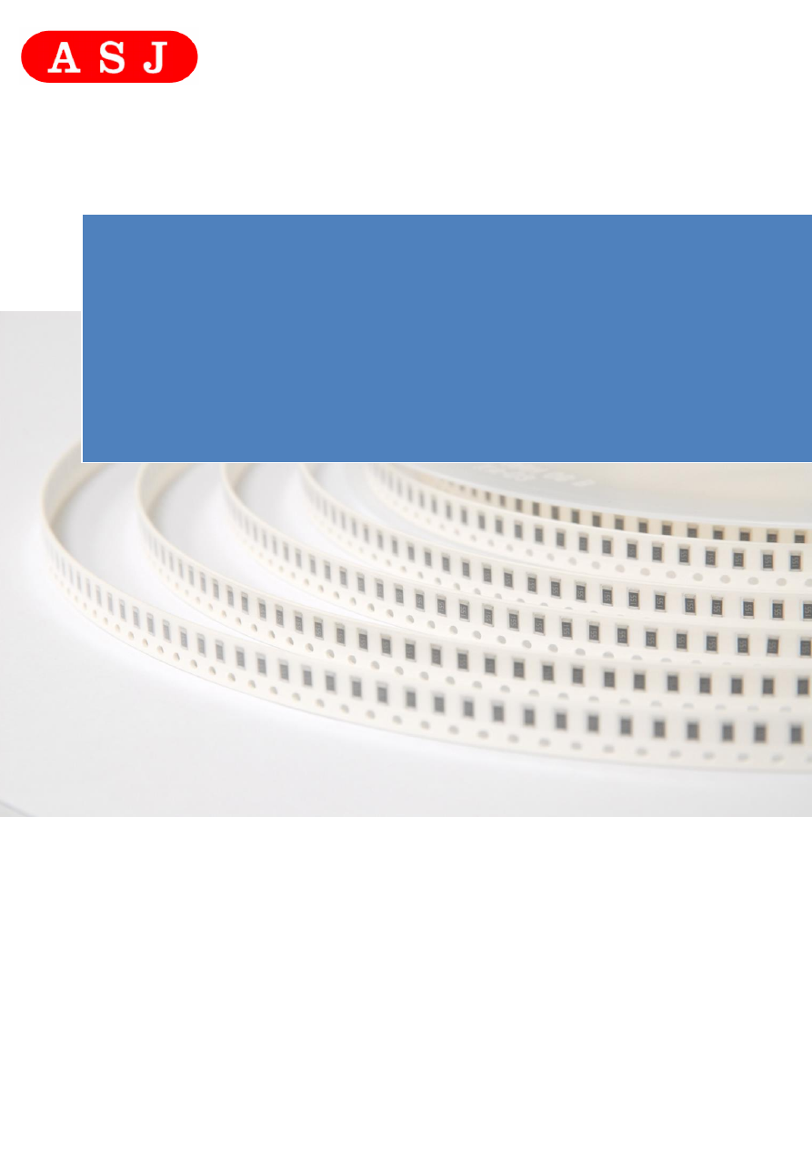
High Power Rating Chip Resistor
CPW Series
0.1% TO 5%, TCR -200 TO +400
SIZE: 0201/0402/0603/0805/1206/1210/2010/2512
RoHs Compliant
Towards Excellence in
Quality, Service & Innovation
Product Specification – Oct 24, 2017 V.5
DATA SHEET
High Power Rating Chip Resistor
CPW Series
0.1% TO 5%, TCR -200 TO +400
SIZE: 0201/0402/0603/0805/1206/1210/2010/2512
RoHs Compliant
Towards Excellence in
Quality, Service & Innovation