background image

High Precision Bulk Metal

®

 Foil Surface Mount Voltage Divider, 

TCR Tracking of < 0.5 ppm/°C, Tolerance Match of 0.01 %

and Stability of ± 0.005 % (50 ppm)

DSM

Vishay Foil Resistors


Document Number: 63088

For any questions, contact: 

foil@vishaypg.com

www.vishayfoilresistors.com

Revision: 22-Apr-2013

1

INTRODUCTION

Bulk Metal

®

 Foil (BMF) technology out-performs all other 

resistor technologies available today for applications that 
require high precision and high stability.

This technology has been invented, patented and pioneered 
by Vishay Foil Resistors (VFR). Products based on this 
technology are the most suitable for a wide range of 
appilcations.

BMF technology allows the production of customer oriented 
products designed to satisfy challenging and specific 
technical requirements. Model DSM offers low TCR (both 
absolute and tracking), excellent load life stability, tight 
tolerance, excellent ratio stability, and low current noise, all in 
one package.

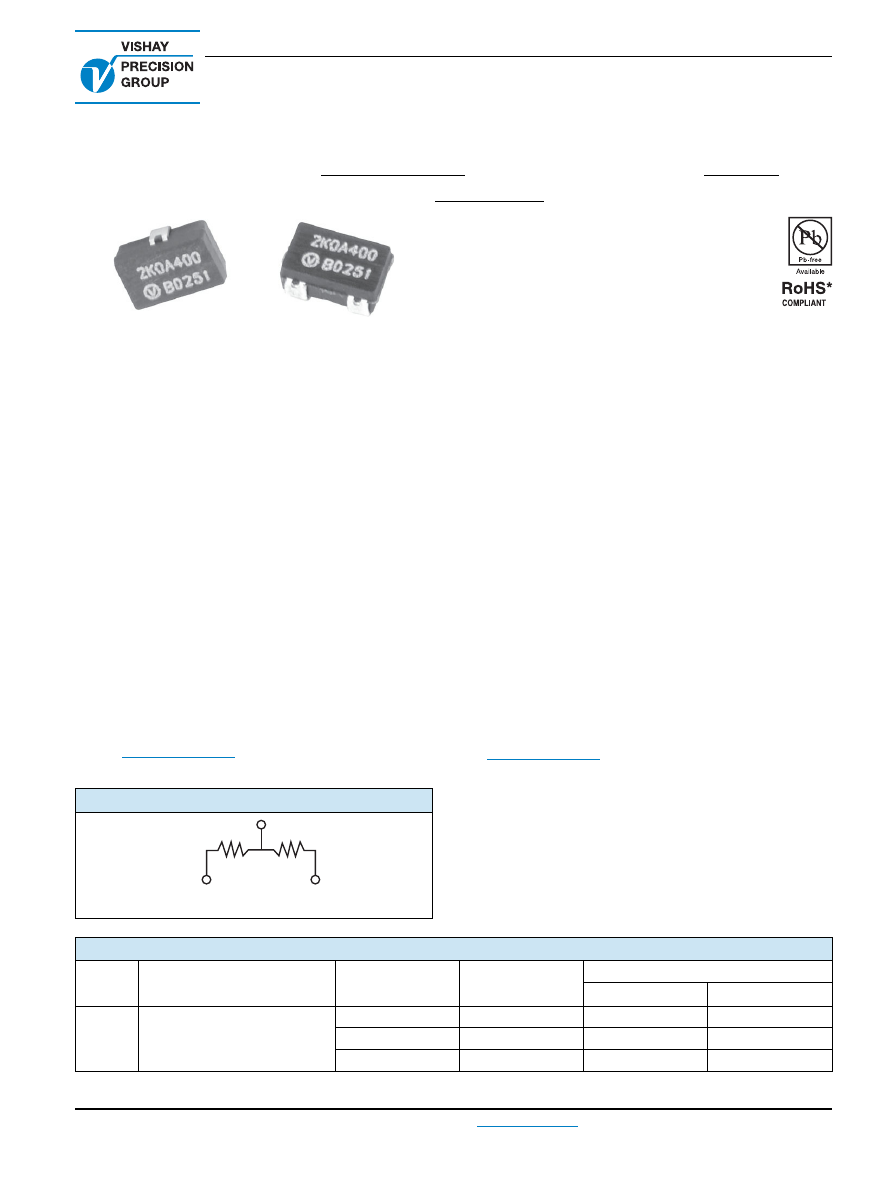
The DSM surface mount divider provides a matched pair of 
Bulk Metal

®

 Foil resistors in a small epoxy molded package. 

The electrical specification of this integrated construction 
offers improved performance and better real estate utilization 
over discrete resistors and matched pairs.

VFR’s application engineering department is available to 
advise and make recommendations. For non-standard 
technical requirements and special applications, please 
contact 

foil@vishaypg.com

.

FIGURE 1 - SCHEMATIC

OPTION 1

SAME OHMIC VALUE,

SAME ABSOLUTE TOLERANCE

R

1

OPTION 2

RESISTOR PAIR

R

1

/R

2

 - DIFFERENT VALUES

R

2

FEATURES

Temperature coefficient of resistance (TCR):

Absolute: 2 ppm/°C typical

(- 55 °C to + 125 °C, + 25 °C ref.)

Tracking: 0.5 ppm/°C typical

Tolerance: absolute: ± 0.02 %; match: 0.01 %

Power rating: to 70 °C: entire package: 0.1 W

each resistor: 0.05 W

Ratio stability: 0.005 % (0.05 W at 70 °C, 2000 h)

Resistance range: 100 

 to 12 k

 per resistor

Large variety of resistance ratios: 1:120

Vishay Foil resistors are not restricted to standard 
values/ratios; specific “as required” values/ratios can be 
supplied at no extra cost or delivery (e.g. 1K234/2K345 vs. 
1K/2K)

Thermal stabilization time < 1 s (nominal value achieved 
within 10 ppm of steady state value)

Electrostatic discharge (ESD) at least to 25kV

Short time overload: 0.005 %

Non inductive, non capacitive design

Rise time: 1 ns effectively no ringing

Current noise: < 0.010 µV

RMS

/V  of applied voltage 

( - 40 dB)

Voltage coefficient: 0.1 ppm/V

Non inductive: 0.08 µH

Non hot spot design

Terminals: silver coated copper alloy (see Table 5)

Compliant to RoHS directive 2002/95/EC

Prototype quantities available in just 5 working days 
or sooner. For more information, please contact 

foil@vishaypg.com

For better performances, please see DSMZ datasheet 
(Z-Foil)

TABLE 1 - MODEL DSM SPECIFICATIONS

MODEL

ABSOLUTE TCR

(- 55 °C TO + 125 °C, + 25 °C REF.)

TYPICAL + MAX. SPREAD

RESISTANCE 

RATIO

TCR TRACKING

TOLERANCE

ABSOLUTE

MATCH

DSM

± 2 ppm/°C ± 3 ppm/°C

R1/R2 = 1

1.0 ppm/°C

± 0.02 %

0.01 %

1 < R1/R2 

 10

2.0 ppm/°C

± 0.05 %

0.02 %

10 < R1/R2 

 120

3.0 ppm/°C

± 0.1 %

0.05 %

* Pb containing terminations are not RoHS compliant, exemptions may apply

DSM-html.html
background image

FIGURE 2 - POWER DERATING CURVE

125

- 55

90 

80 

- 60

- 40

- 20

0

20 

40 

60 

80 

100  120 

70

140

70 

60 

50 

40 

30 

20 

10 

100

110

Ambient Temperature  (°C) 

P

er

cent o

f Rated 

W

atta

g

DSM

Vishay Foil Resistors


www.vishayfoilresistors.com

For any questions, contact: 

foil@vishaypg.com

Document Number: 63088

2

Revision: 22-Apr-2013

FIGURE 4 - TRIMMING TO VALUES

(Conceptual Illustration)

Mutual Inductance
Reduction due
to Opposing
Current in
Adjacent Lines

Current Path

Before Trimming

Note:

 Foil shown in black, etched spaces in white

Interloop Capacitance
Reduction in Series

Trimming Process

Removes this Material

from Shorting Strip Area

Changing Current Path

and Increasing

Resistance

Current Path

After Trimming

FIGURE 3 - RECOMMENDED LAND 

0.063 ± 0.004

(1.6 ± 0.1)

0.100 ± 0.004

(2.54 ± 0.1)

0.040 ± 0.004

(1.02 ± 0.1)

0.071 ± 0.004

(1.8 ± 0.1)

0.100 ± 0.004

(2.54 ± 0.1)

0.035 ± 0.004

(0.89 ± 0.1)

FIGURE 5 - TYPICAL RESISTANCE/ 

TEMPERATURE CURVE

(For more details, see table 1)

- 55

- 50

- 25

0

+ 25

+ 50

+ 75

+ 100

+ 125

± 2 ppm/°C
(+ 25 °C reference)

+ 150

+ 100

+ 50

0

- 50

- 100

- 150

- 200

Δ

R

R

(ppm)

Ambient Temperature  (°C)

FIGURE 6 - DIMENSIONS AND IMPRINTING

w

P

P

t

H

TH

L

S

TW

TW

W

E

I

V


T

N

O

R

F

W

E

I

V


E

D

I

S

STAND OFF

TW

BOTTOM VIEW

1

2

3

10K Q 10K

(1) (2)

B0219

VALUE R1

RATIO TOLERANCE CODE

VALUE R2

DATE CODE

TOP VIEW

1

2

3

Notes

(1)

  If the resistance value of R1 and R2 

contains more than 6 characters 
together, the VCODE will be printed 
instead (see Resistance Value Code 
List for Popular Ratios Table) 
followed by the ratio tolerance code. 

(2)

  R1—between PIN1 and PIN3

R2—between PIN2 and PIN3.

DIMENSIONS

L

W

H

TW 

TH 

INCHES

0.160 ± 0.008 0.106 ± 0.008 0.063 ± 0.008 0.031 ± 0.005  0.031 ± 0.004  0.043 ± 0.008  0.100 ± 0.008  0.005 ± 0.002 

MILLIMETERS

4.06 ± 0.20

2.69 ± 0.20

1.60 ± 0.20

0.79 ± 0.13 

0.79 ± 0.10

1.09 ± 0.20

2.54 ± 0.20

0.13 ± 0.05 

DSM-html.html
background image

TABLE 3 - PERFORMANCE SPECIFICATIONS

 (Test Method Per MIL-PRF-914)

SPECIFICATIONS

TYPICAL LIMITS

Power Rating

 at 70 °C 

Entire package: 0.1 W 
Each resistor: 0.05 W

Maximum Working Voltage

 (each resistor) 

25 V 

Working Temperature Range

- 65 °C to + 125 °C 

Thermal Shock


R = 0.01 % (100 ppm) 

25 x (- 65 °C to + 125 °C) 

Ratio = 0.005 % (50 ppm) 

Thermal Shock 

5 x (- 65 °C to + 125 °C) and 

R = 0.015 % (150 ppm) 

Power Conditioning 

Ratio = 0.01 % (100 ppm) 

1.5 rated power at 25 °C, 100 h

DWV

 atmospheric pressure, 200 V (A.C.), 1 min

Successfully passed 

Insulation Resistance

 100 V (D.C.), 1 min

> 10

4

 M


Resistance to Soldering Heat 

R = 0.01 % (100 ppm) 

Ratio = 0.005 % (50 ppm) 

Moisture Resistance 

R = 0.02 % (200 ppm) 

+ 65 °C to - 10 °C; 90 % to 98 % RH; 0.1 x rated power, 240 h

Ratio = 0.005 % (50 ppm) 

Shock (Specified Pulse)

R = 0.005 % (50 ppm) 

100 G 

Ratio = 0.0025 % (25 ppm) 

Vibration, High Frequency 

R = 0.01 % (100 ppm) 

(10 Hz to 2000 Hz), 20 G 

Ratio = 0.005 % (50 ppm) 

High Temperature Exposure 

R = 0.01 % (100 ppm) 

100 h at 125 °C

Ratio = 0.005 % (50 ppm) 

Low Temperature Storage 

R = 0.005 % (50 ppm) 

24 h at - 65 °C 

Ratio = 0.005 % (50 ppm) 

Load Life Stability 

R = 0.005 % (50 ppm) 

2000 h at + 70 °C; rated power 

Ratio = 0.005 % (50 ppm) 

Short Time Overload 

R = 0.005 % (50 ppm) 

6.25 x rated power; 5 s

Ratio = 0.0025 % (25 ppm) 

Low Temperature Operation 

R = 0.005 % (50 ppm) 

Ratio = 0.0025 % (25 ppm) 

Weight 

0.04 g 

DSM

Vishay Foil Resistors


Document Number: 63088

For any questions, contact: 

foil@vishaypg.com

www.vishayfoilresistors.com

Revision: 22-Apr-2013

3

FIGURE 7 - DSM 10K/10K, 20 UNITS, LOAD LIFE 

0.05 W each value, at + 70 °C

+ 60

+ 40

+ 50

+ 30

+ 20

0

- 10

- 30

- 40

- 50

Δ

Ratio (ppm)

Time (h)

250

500

1000

2000

+ 10

- 20

DSM-html.html
background image

DSM

Vishay Foil Resistors


www.vishayfoilresistors.com

For any questions, contact: 

foil@vishaypg.com

Document Number: 63088

4

Revision: 22-Apr-2013

FIGURE 8 - DSM 10K/10K, 20 UNITS, HIGH TEMPERATURE EXPOSURE,

100 h at 125 °C, followed by low temperature storage, 24 h at - 65 °C

+ 80

+ 60

+ 40

0

- 20

- 40

Δ

Ratio (ppm)

High Temperature Exposure

Low Temperature Storage

+ 20

TABLE 4 - RESISTANCE VALUE CODE LIST FOR POPULAR RATIOS

(other values available upon request)

VCODES

R1/R2

RATIO

R1

R2

VCODES

R1/R2

RATIO

R1

R2

V0052

100

10K

100R

V0080

2.5

1K

400R

V0065

50

10K

200R

V0081

500R

200R

V0066

5K

100R

V0082

2

10K

5K

V0067
V0068

25

10K

5K

400R
200R

V0083

2K

1K

V0084

1K

500R

V0085

400R

200R

V0069

20

10K

500R

V0086

200R

100R

V0070

2K

100R

V0087

1.25

500R

400R

V0071

10

10K

1K

V0001
V0002
V0059
V0004
V0091
V0090
V0089
V0088

1

10K

5K
2K
1K

500R
400R
200R
100R

10K

5K
2K
1K

500R
400R
200R
100R

V0072

2K

200R

V0073

1K

100R

V0074

5

5K

1K

V0075

2K

400R

V0076

1K

200R

V0077

500R

100R

V0246

4

10K

2K5

V0078

2K

500R

V0079

400R

100R

DSM-html.html
background image

TABLE 5 - GLOBAL PART NUMBER INFORMATION

 (1)

NEW GLOBAL PART NUMBER:  Y1485V0067BA9W  (preferred part number format)

DENOTES PRECISION

VCODE

TOLERANCE MATCH

PACKAGING

Y

RESISTANCE

VALUE CODE

T

= 0.01 %

Q

= 0.02 %

A

= 0.05 %

R

= tape and reel

W

= waffle pack

L

= bulk pack

PRODUCT CODE

RESISTANCE TOLERANCE

CHARACTERISTICS

1485

 = DSM

Q

 = ± 0.02 %

A

 = ± 0.05 %

B

 = ± 0.10 %

0

 = silver plated or HSD tin/lead

9

 = silver plated or HSD lead (Pb)-free

1 to 999

 = custom

FOR EXAMPLE: ABOVE GLOBAL ORDER Y1485 V0067 B A 9 W:
TYPE: DSM

VALUES: 10K/400R

ABSOLUTE TOLERANCE: ± 0.1 %

TOLERANCE MATCH: 0.05 %

TERMINATION:  silver plated or HSD lead (Pb)-free 

AER: standard

PACKAGING: waffle pack

HISTORICAL PART NUMBER:  DSM  10K 400R  TCR2  B  A   S   W  (will continue to be used)

DSM

10K 400R

TCR2

B

A

S

W

MODEL

OHMIC VALUE

TCR

CHARACTERISTIC

ABSOLUTE

TOLERANCE

TOLERANCE

MATCH

TERMINATION

PACKAGING

R

1

 = 10 k

R

2

 = 400 

Q

 = ± 0.02 %

A

 = ± 0.05 %

B

 = ± 0.10 %

= 0.01 %

= 0.02 %

= 0.05 %

S

 = silver plated or 

HSD lead 

(Pb)-free

B

 = silver plated or 

HSD tin/lead

T

= tape and reel

W

= waffle pack

B

= bulk pack

DSM

Vishay Foil Resistors


Document Number: 63088

For any questions, contact: 

foil@vishaypg.com

www.vishayfoilresistors.com

Revision: 22-Apr-2013

5

Note

(1)

For non-standard requests or additional values, please contact application engineering.

4

8

5

V

0

6

7

0

Y

1

A

9

B

W

DSM-html.html
background image

Vishay Precision Group

Document No.: 63999

Revision: 27-Apr-2011

www.vishaypg.com

1

Legal Disclaimer Notice

Disclaimer

Legal Disclaimer Notice

Disclaimer

Document No.: 63999

Revision: 27-Apr-2011

ALL PRODUCTS, PRODUCT SPECIFICATIONS AND DATA ARE SUBJECT TO CHANGE WITHOUT NOTICE.

Vishay Precision Group, Inc., its affiliates, agents, and employees, and all persons acting on its or their 
behalf (collectively, “Vishay Precision Group”), disclaim any and all liability for any errors, inaccuracies or 
incompleteness contained herein or in any other disclosure relating to any product.

The product specifications do not expand or otherwise modify Vishay Precision Group’s terms and 
conditions of purchase, including but not limited to, the warranty expressed therein.

Vishay Precision Group makes no warranty, representation or guarantee other than as set forth in the terms 
and conditions of purchase. 

To the maximum extent permitted by applicable law, Vishay Precision 

Group disclaims (i) any and all liability arising out of the application or use of any product, (ii) any and 
all liability, including without limitation special, consequential or incidental damages, and (iii) any and 
all implied warranties, including warranties of fitness for particular purpose, non-infringement and 
merchantability.

Information provided in datasheets and/or specifications may vary from actual results in different 
applications and performance may vary over time. Statements regarding the suitability of products for 
certain types of applications are based on Vishay Precision Group’s knowledge of typical requirements that 
are often placed on Vishay Precision Group products. It is the customer’s responsibility to validate that a 
particular product with the properties described in the product specification is suitable for use in a particular 
application.

No license, express, implied, or otherwise, to any intellectual property rights is granted by this document, or 
by any conduct of Vishay Precision Group.

The products shown herein are not designed for use in life-saving or life-sustaining applications unless 
otherwise expressly indicated. Customers using or selling Vishay Precision Group products not expressly 
indicated for use in such applications do so entirely at their own risk and agree to fully indemnify Vishay 
Precision Group for any damages arising or resulting from such use or sale. Please contact authorized 
Vishay Precision Group personnel to obtain written terms and conditions regarding products designed for 
such applications.

Product names and markings noted herein may be trademarks of their respective owners.