Altera Corporation
Section I–1
Preliminary
Section I. Cyclone FPGA
Family Data Sheet
This section provides designers with the data sheet specifications for
Cyclone devices. The chapters contain feature definitions of the internal
architecture, configuration and JTAG boundary-scan testing information,
DC operating conditions, AC timing parameters, a reference to power
consumption, and ordering information for Cyclone devices.
This section contains the following chapters:
■
Chapter 1. Introduction
■
Chapter 2. Cyclone Architecture
■
Chapter 3. Configuration & Testing
■
Chapter 4. DC & Switching Characteristics
■
Chapter 5. Reference & Ordering Information
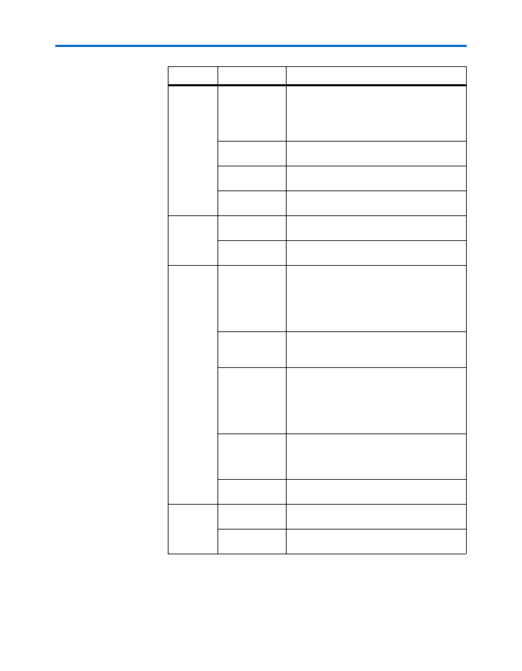
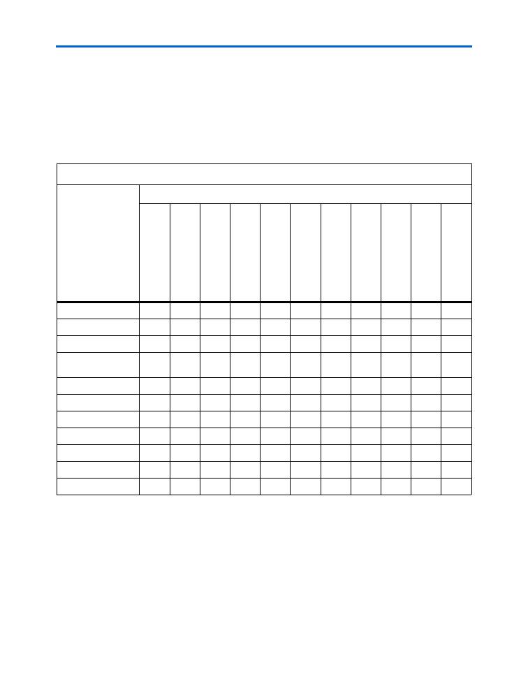
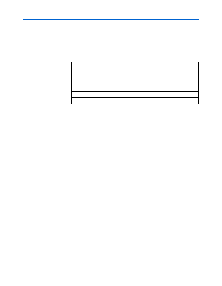
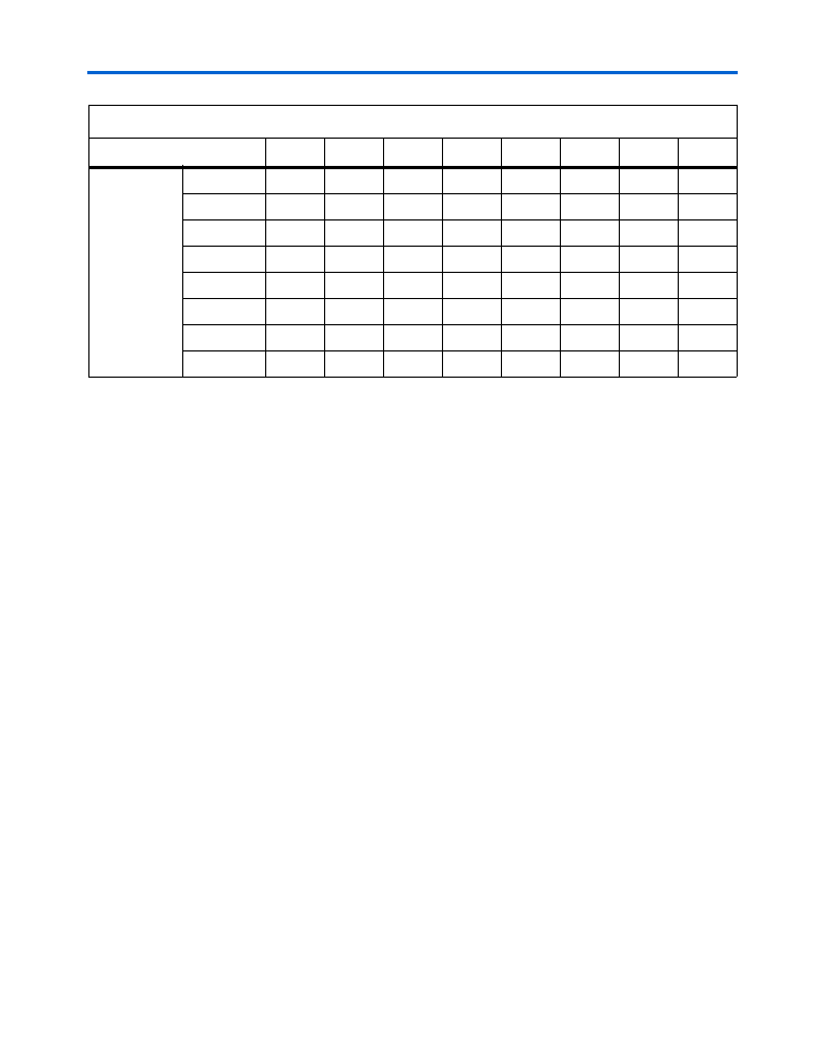
Revision History
The table below shows the revision history for
Chapters 1
through
5
.
Chapter(s)
Date / Version
Changes Made
1
October 2003
v1.2
Added 64-bit PCI support information.
September 2003
v1.1
Updated LVDS data rates to 640 Mbps from
311 Mbps.
Updated RSDS feature information.
May 2003
v1.0
Added document to Cyclone Device Handbook.
FPGA_cyc-html.html
Section I–2
Altera Corporation
Preliminary
Cyclone FPGA Family Data Sheet
Cyclone Device Handbook, Volume 1
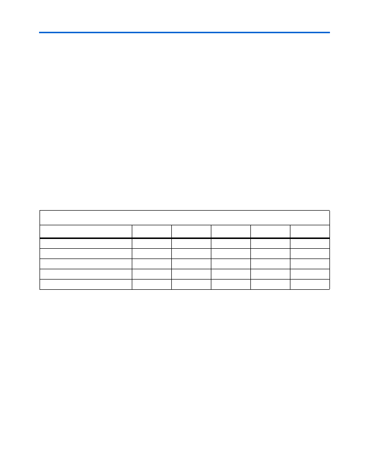
2
February 2005
v1.3
Updated JTAG chain limits. Added test vector
information.
Corrected Figure 2-12.
Added a note to Tables 2-17 through 2-21
regarding violating the setup or hold time.
October 2003
v1.2
Updated phase shift information.
Added 64-bit PCI support information.
September 2003
v1.1
Updated LVDS data rates to 640 Mbps from
311 Mbps.
May 2003
v1.0
Added document to Cyclone Device Handbook.
3
February 2005
V1.1
Updated JTAG chain limits. Added information
concerning test vectors.
May 2003
v1.0
Added document to Cyclone Device Handbook.
4
February 2005
v1.4
Updated information on Undershoot voltage.
Updated Table 4-2.
Updated Table 4-3.
Updated the undershoot voltage from 0.5 V to
2.0 V in Note 3 of Table 4-16.
Updated Table 4-17.
January 2004
v.1.3
Added extended-temperature grade device
information. Updated Table 4-2.
Updated I
C C 0
information in Table 4-3.
October 2003
v.1.2
Added clock tree information in Tab;e 4-19.
Finalized timing information for EP1C3 and
EP1C12 devices. Updated timing information in
Tables 4-25 through 4-26 and Tables 4-30
through 4-51.
Updated PLL specifications in Table 4-52.
July 2003
v1.1
Updated timing information. Timing finalized for
EP1C6 and EP1C20 devices. Updated
performance information. Added PLL Timing
section.
May 2003
v1.0
Added document to Cyclone Device Handbook.
5
February 2005
v1.1
Updated Figure 5-1.
May 2003
v1.0
Added document to Cyclone Device Handbook.
Chapter(s)
Date / Version
Changes Made
FPGA_cyc-html.html
FPGA_cyc-html.html
1–2
Altera
Corporation
Preliminary
October 2003
Cyclone Device Handbook, Volume 1
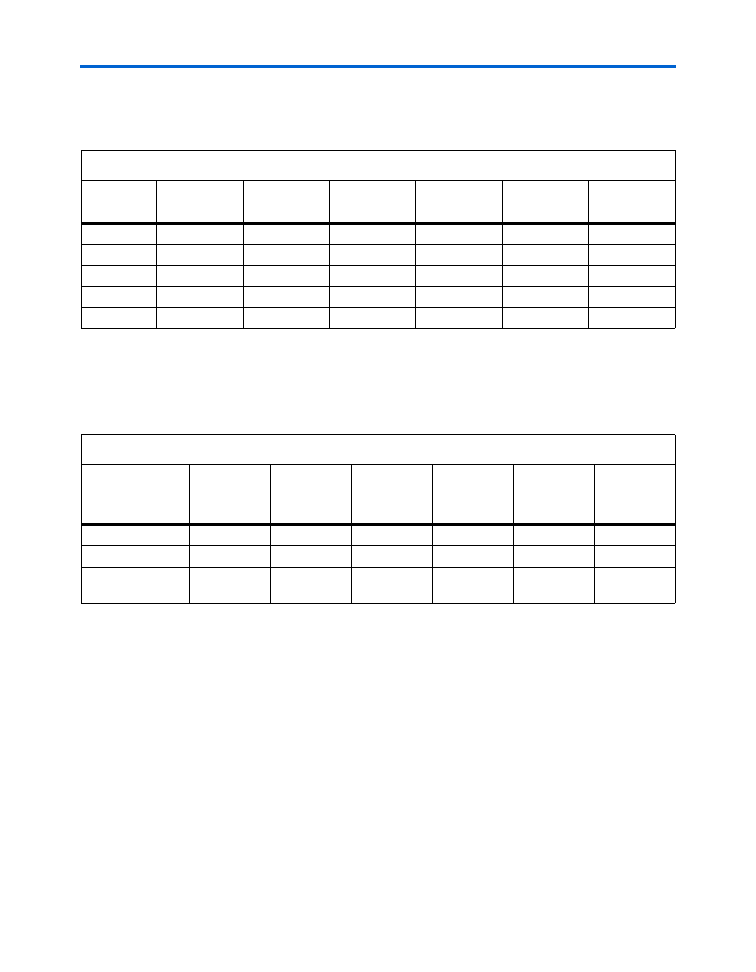
Features
The Cyclone device family offers the following features:
■
2,910 to 20,060 LEs, see
Table 1–1
■
Up to 294,912 RAM bits (36,864 bytes)
■
Supports configuration through low-cost serial configuration device
■
Support for LVTTL, LVCMOS, SSTL-2, and SSTL-3 I/O standards
■
Support for 66- and 33-MHz, 64- and 32-bit PCI standard
■
High-speed (640 Mbps) LVDS I/O support
■
Low-speed (311 Mbps) LVDS I/O support
■
311-Mbps RSDS I/O support
■
Up to two PLLs per device provide clock multiplication and phase
shifting
■
Up to eight global clock lines with six clock resources available per
logic array block (LAB) row
■
Support for external memory, including DDR SDRAM (133 MHz),
FCRAM, and single data rate (SDR) SDRAM
■
Support for multiple intellectual property (IP) cores, including
Altera
®
MegaCore
®
functions and Altera Megafunctions Partners
Program (AMPP
SM
) megafunctions.
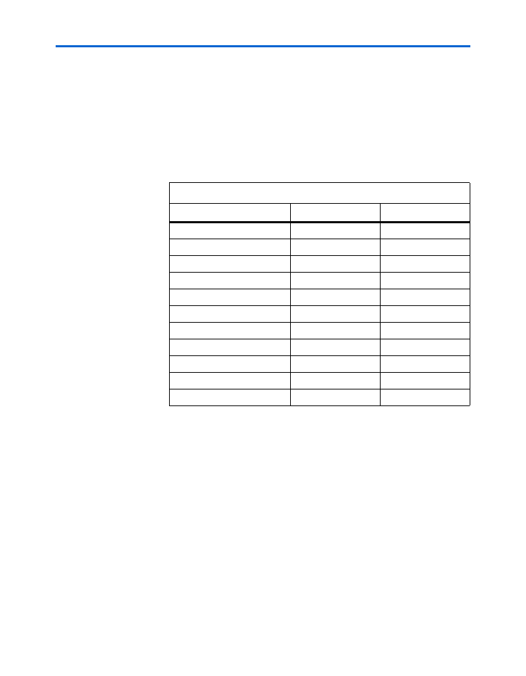
Table 1–1. Cyclone Device Features
Feature
EP1C3
EP1C4
EP1C6
EP1C12
EP1C20
LEs
2,910
4,000
5,980
12,060
20,060
M4K RAM blocks (128
×
36 bits)
13
17
20
52
64
Total RAM bits
59,904
78,336
92,160
239,616
294,912
PLLs
1
2
2
2
2
Maximum user I/O pins
(1)
104
301
185
249
301
Note to
Table 1–1
:
(1)
This parameter includes global clock pins.
FPGA_cyc-html.html
Altera Corporation
1–3
October 2003
Preliminary
Features
Cyclone devices are available in quad flat pack (QFP) and space-saving
FineLine BGA
®
packages (see
Table 1–2
through
1–3
).
Table 1–2. Cyclone Package Options & I/O Pin Counts
Device
100-Pin TQFP
(1)
144-Pin TQFP
(1)
,
(2)
240-Pin PQFP
(1)
256-Pin
FineLine BGA
324-Pin
FineLine BGA
400-Pin
FineLine BGA
EP1C3
65
104
EP1C4
249
301
EP1C6
98
185
185
EP1C12
173
185
249
EP1C20
233
301
Notes to
Table 1–2
:
(1)
TQFP: thin quad flat pack.
PQFP: plastic quad flat pack.
(2)
Cyclone devices support vertical migration within the same package (i.e., designers can migrate between the
EP1C3 device in the 144-pin TQFP package and the EP1C6 device in the same package)
Table 1–3. Cyclone QFP & FineLine BGA Package Sizes
Dimension
100-Pin
TQFP
144-Pin
TQFP
240-Pin
PQFP
256-Pin
FineLine
BGA
324-Pin
FineLine
BGA
400-Pin
FineLine
BGA
Pitch (mm)
0.5
0.5
0.5
1.0
1.0
1.0
Area (mm
2
)
256
484
1,024
289
361
441
Length
×
width
(mm
×
mm)
16
×
16
22
×
22
34.6
×
34.6
17
×
17
19
×
19
21
×
21
FPGA_cyc-html.html

1–4
Altera
Corporation
Preliminary
October 2003
Cyclone Device Handbook, Volume 1
FPGA_cyc-html.html

Altera Corporation
2–1
February 2005
Preliminary
2. Cyclone Architecture
Functional
Description
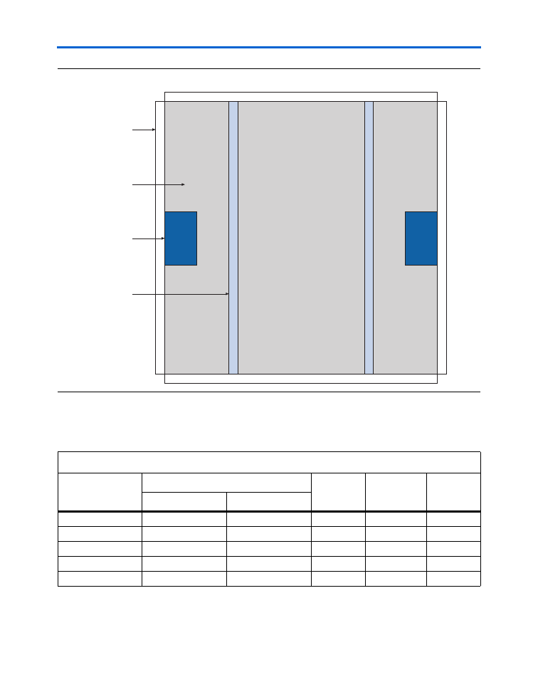
Cyclone devices contain a two-dimensional row- and column-based
architecture to implement custom logic. Column and row interconnects of
varying speeds provide signal interconnects between LABs and
embedded memory blocks.
The logic array consists of LABs, with 10 LEs in each LAB. An LE is a
small unit of logic providing efficient implementation of user logic
functions. LABs are grouped into rows and columns across the device.
Cyclone devices range between 2,910 to 20,060 LEs.
M4K RAM blocks are true dual-port memory blocks with 4K bits of
memory plus parity (4,608 bits). These blocks provide dedicated true
dual-port, simple dual-port, or single-port memory up to 36-bits wide at
up to 200 MHz. These blocks are grouped into columns across the device
in between certain LABs. Cyclone devices offer between 60 to 288 Kbits of
embedded RAM.
Each Cyclone device I/O pin is fed by an I/O element (IOE) located at the
ends of LAB rows and columns around the periphery of the device. I/O
pins support various single-ended and differential I/O standards, such as
the 66- and 33-MHz, 64- and 32-bit PCI standard and the LVDS I/O
standard at up to 640 Mbps. Each IOE contains a bidirectional I/O buffer
and three registers for registering input, output, and output-enable
signals. Dual-purpose DQS, DQ, and DM pins along with delay chains
(used to phase-align DDR signals) provide interface support with
external memory devices such as DDR SDRAM, and FCRAM devices at
up to 133 MHz (266 Mbps).
Cyclone devices provide a global clock network and up to two PLLs. The
global clock network consists of eight global clock lines that drive
throughout the entire device. The global clock network can provide
clocks for all resources within the device, such as IOEs, LEs, and memory
blocks. The global clock lines can also be used for control signals. Cyclone
PLLs provide general-purpose clocking with clock multiplication and
phase shifting as well as external outputs for high-speed differential I/O
support.
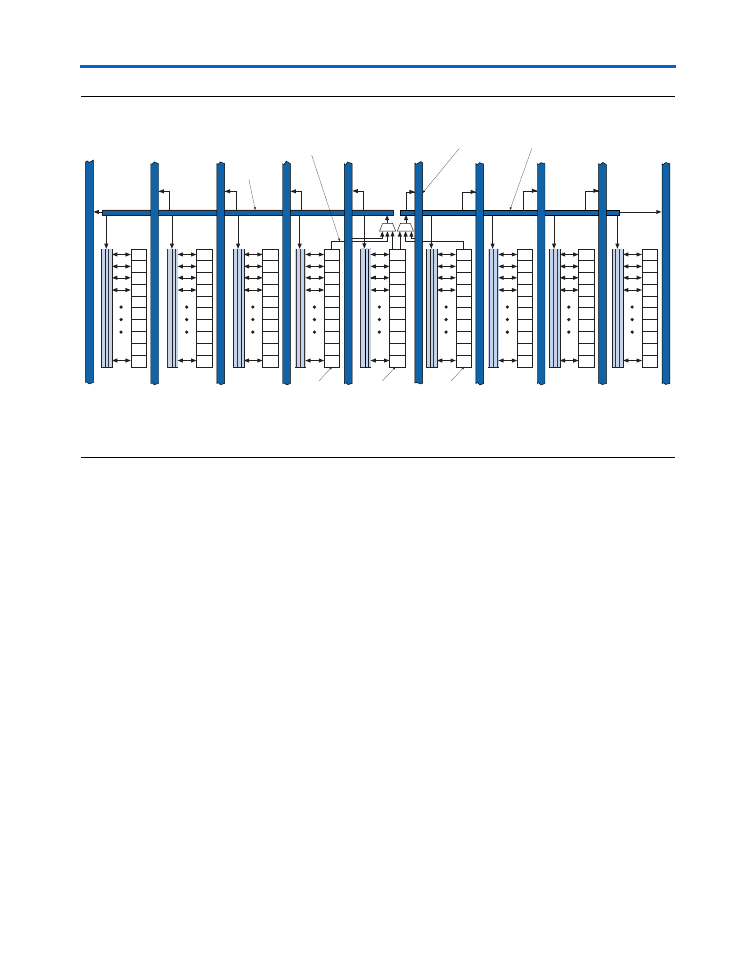
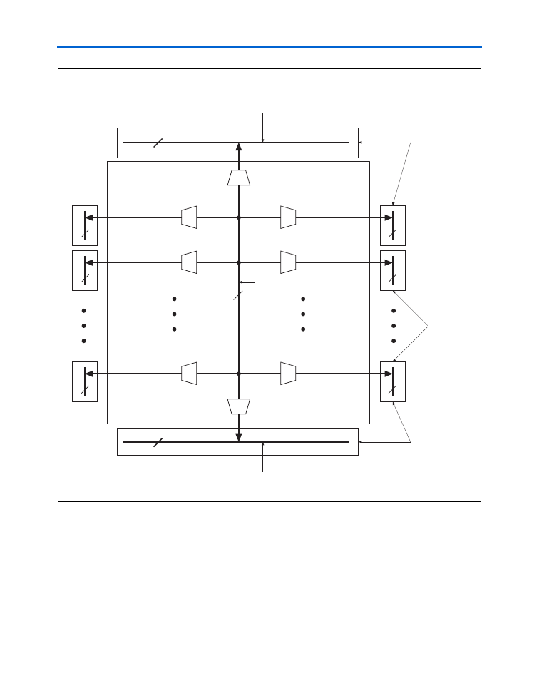
Figure 2–1
shows a diagram of the Cyclone EP1C12 device.
C51002-1.3
FPGA_cyc-html.html
2–2
Altera
Corporation
Preliminary
February 2005
Cyclone Device Handbook, Volume 1
Figure 2–1. Cyclone EP1C12 Device Block Diagram
The number of M4K RAM blocks, PLLs, rows, and columns vary per
device.
Table 2–1
lists the resources available in each Cyclone device.
Logic Array
PLL
IOEs
M4K Blocks
EP1C12 Device
Table 2–1. Cyclone Device Resources
Device
M4K RAM
PLLs
LAB Columns
LAB Rows
Columns
Blocks
EP1C3
1
13
1
24
13
EP1C4
1
17
2
26
17
EP1C6
1
20
2
32
20
EP1C12
2
52
2
48
26
EP1C20
2
64
2
64
32
FPGA_cyc-html.html
Altera Corporation
2–3
February 2005
Preliminary
Logic Array Blocks
Logic Array
Blocks
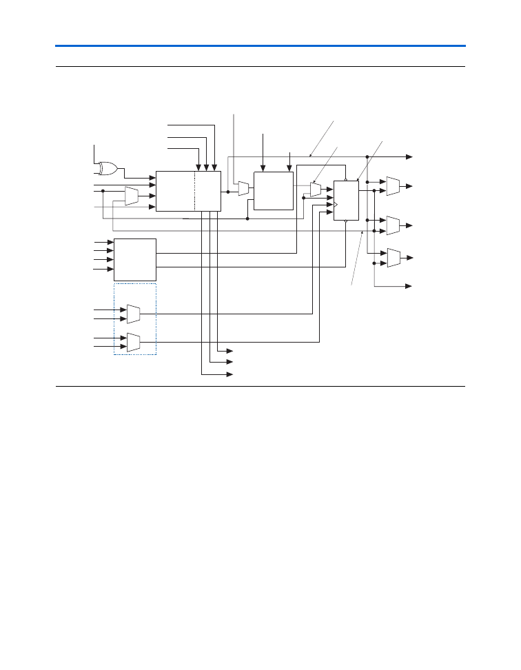
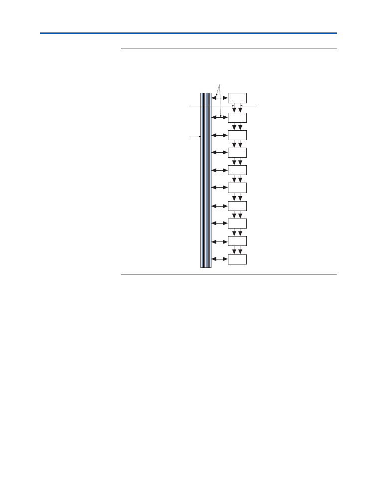
Each LAB consists of 10 LEs, LE carry chains, LAB control signals, a local
interconnect, look-up table (LUT) chain, and register chain connection
lines. The local interconnect transfers signals between LEs in the same
LAB. LUT chain connections transfer the output of one LE's LUT to the
adjacent LE for fast sequential LUT connections within the same LAB.
Register chain connections transfer the output of one LE's register to the
adjacent LE's register within an LAB. The Quartus
®
II Compiler places
associated logic within an LAB or adjacent LABs, allowing the use of
local, LUT chain, and register chain connections for performance and area
efficiency.
Figure 2–2
details the Cyclone LAB.
Figure 2–2. Cyclone LAB Structure
LAB Interconnects
The LAB local interconnect can drive LEs within the same LAB. The LAB
local interconnect is driven by column and row interconnects and LE
outputs within the same LAB. Neighboring LABs, PLLs, and M4K RAM
blocks from the left and right can also drive an LAB's local interconnect
through the direct link connection. The direct link connection feature
minimizes the use of row and column interconnects, providing higher
Direct link
interconnect from
adjacent block
Direct link
interconnect to
adjacent block
Row Interconnect
Column Interconnect
Local Interconnect
LAB
Direct link
interconnect from
adjacent block
Direct link
interconnect to
adjacent block
FPGA_cyc-html.html
2–4
Altera
Corporation
Preliminary
February 2005
Cyclone Device Handbook, Volume 1
performance and flexibility. Each LE can drive 30 other LEs through fast
local and direct link interconnects.
Figure 2–3
shows the direct link
connection.
Figure 2–3. Direct Link Connection
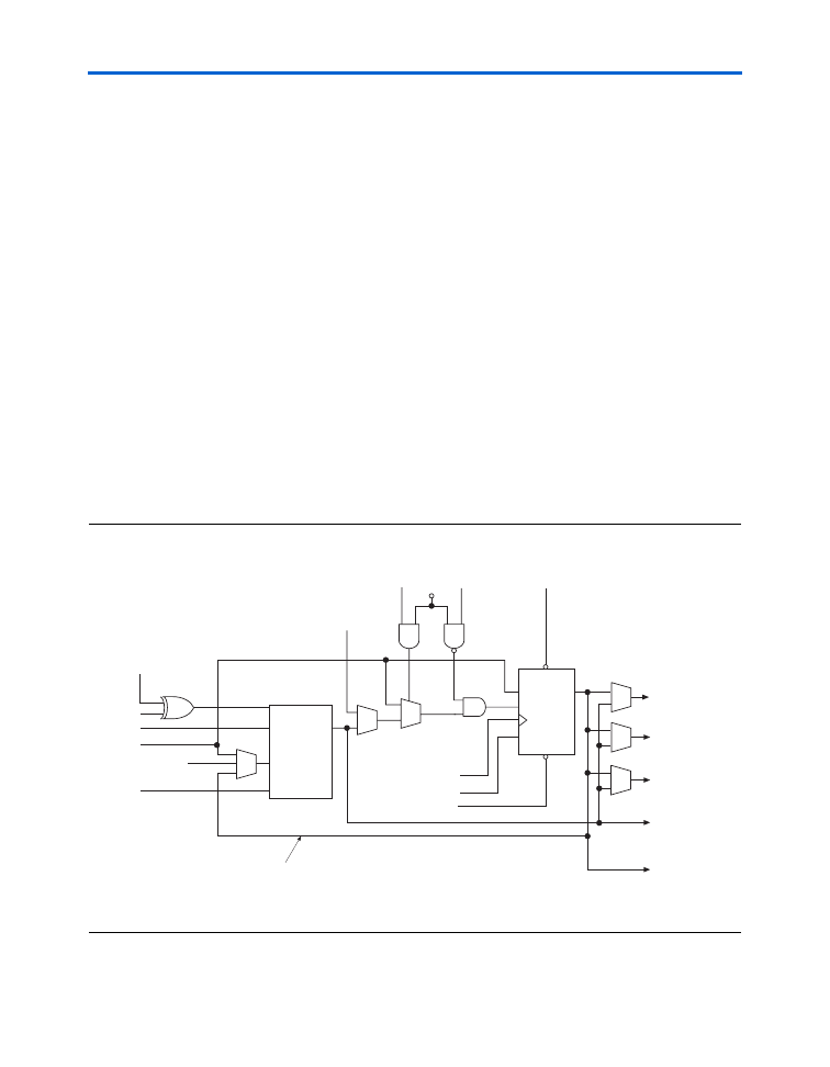
LAB Control Signals
Each LAB contains dedicated logic for driving control signals to its LEs.
The control signals include two clocks, two clock enables, two
asynchronous clears, synchronous clear, asynchronous preset/load,
synchronous load, and add/subtract control signals. This gives a
maximum of 10 control signals at a time. Although synchronous load and
clear signals are generally used when implementing counters, they can
also be used with other functions.
Each LAB can use two clocks and two clock enable signals. Each LAB's
clock and clock enable signals are linked. For example, any LE in a
particular LAB using the
labclk1
signal will also use
labclkena1
. If
the LAB uses both the rising and falling edges of a clock, it also uses both
LAB-wide clock signals. De-asserting the clock enable signal will turn off
the LAB-wide clock.
Each LAB can use two asynchronous clear signals and an asynchronous
load/preset signal. The asynchronous load acts as a preset when the
asynchronous load data input is tied high.
LAB
Direct link
interconnect
to right
Direct link interconnect from
right LAB, M4K memory
block, PLL, or IOE output
Direct link interconnect from
left LAB, M4K memory
block, PLL, or IOE output
Local
Interconnect
Direct link
interconnect
to left
FPGA_cyc-html.html
Altera Corporation
2–5
February 2005
Preliminary
Logic Elements
With the LAB-wide
addnsub
control signal, a single LE can implement a
one-bit adder and subtractor. This saves LE resources and improves
performance for logic functions such as DSP correlators and signed
multipliers that alternate between addition and subtraction depending
on data.
The LAB row clocks [5..0] and LAB local interconnect generate the LAB-
wide control signals. The MultiTrack
TM
interconnect's inherent low skew
allows clock and control signal distribution in addition to data.
Figure 2–4
shows the LAB control signal generation circuit.
Figure 2–4. LAB-Wide Control Signals
Logic Elements
The smallest unit of logic in the Cyclone architecture, the LE, is compact
and provides advanced features with efficient logic utilization. Each LE
contains a four-input LUT, which is a function generator that can
implement any function of four variables. In addition, each LE contains a
programmable register and carry chain with carry select capability. A
single LE also supports dynamic single bit addition or subtraction mode
selectable by an LAB-wide control signal. Each LE drives all types of
interconnects: local, row, column, LUT chain, register chain, and direct
link interconnects. See
Figure 2–5
.
labclkena1
labclk2
labclk1
labclkena2
asyncload
or labpre
syncload
Dedicated
LAB Row
Clocks
Local
Interconnect
Local
Interconnect
Local
Interconnect
Local
Interconnect
Local
Interconnect
Local
Interconnect
labclr1
labclr2
synclr
addnsub
6
FPGA_cyc-html.html
2–6
Altera
Corporation
Preliminary
February 2005
Cyclone Device Handbook, Volume 1
Figure 2–5. Cyclone LE
Each LE's programmable register can be configured for D, T, JK, or SR
operation. Each register has data, true asynchronous load data, clock,
clock enable, clear, and asynchronous load/preset inputs. Global signals,
general-purpose I/O pins, or any internal logic can drive the register's
clock and clear control signals. Either general-purpose I/O pins or
internal logic can drive the clock enable, preset, asynchronous load, and
asynchronous data. The asynchronous load data input comes from the
data3
input of the LE. For combinatorial functions, the LUT output
bypasses the register and drives directly to the LE outputs.
Each LE has three outputs that drive the local, row, and column routing
resources. The LUT or register output can drive these three outputs
independently. Two LE outputs drive column or row and direct link
routing connections and one drives local interconnect resources. This
allows the LUT to drive one output while the register drives another
output. This feature, called register packing, improves device utilization
because the device can use the register and the LUT for unrelated
labclk1
labclk2
labclr2
labpre/aload
Carry-In1
Carry-In0
LAB Carry-In
Clock &
Clock Enable
Select
LAB Carry-Out
Carry-Out1
Carry-Out0
Look-Up
Table
(LUT)
Carry
Chain
Row, column,
and direct link
routing
Row, column,
and direct link
routing
Programmable
Register
PRN/ALD
CLRN
D
Q
ENA
Register Bypass
Packed
Register Select
Chip-Wide
Reset
labclkena1
labclkena2
Synchronous
Load and
Clear Logic
LAB-wide
Synchronous
Load
LAB-wide
Synchronous
Clear
Asynchronous
Clear/Preset/
Load Logic
data1
data2
data3
data4
LUT chain
routing to next LE
labclr1
Local Routing
Register chain
output
ADATA
addnsub
Register
Feedback
Register chain
routing from
previous LE
FPGA_cyc-html.html

Altera Corporation
2–7
February 2005
Preliminary
Logic Elements
functions. Another special packing mode allows the register output to
feed back into the LUT of the same LE so that the register is packed with
its own fan-out LUT. This provides another mechanism for improved
fitting. The LE can also drive out registered and unregistered versions of
the LUT output.
LUT Chain & Register Chain
In addition to the three general routing outputs, the LEs within an LAB
have LUT chain and register chain outputs. LUT chain connections allow
LUTs within the same LAB to cascade together for wide input functions.
Register chain outputs allow registers within the same LAB to cascade
together. The register chain output allows an LAB to use LUTs for a single
combinatorial function and the registers to be used for an unrelated shift
register implementation. These resources speed up connections between
LABs while saving local interconnect resources.
“MultiTrack
Interconnect” on page 2–12
for more information on LUT chain and
register chain connections.
addnsub Signal
The LE's dynamic adder/subtractor feature saves logic resources by
using one set of LEs to implement both an adder and a subtractor. This
feature is controlled by the LAB-wide control signal
addnsub
. The
addnsub
signal sets the LAB to perform either A + B or A
−
B. The LUT
computes addition; subtraction is computed by adding the two's
complement of the intended subtractor. The LAB-wide signal converts to
two's complement by inverting the B bits within the LAB and setting
carry-in = 1 to add one to the least significant bit (LSB). The LSB of an
adder/subtractor must be placed in the first LE of the LAB, where the
LAB-wide
addnsub
signal automatically sets the carry-in to 1. The
Quartus II Compiler automatically places and uses the adder/subtractor
feature when using adder/subtractor parameterized functions.
LE Operating Modes
The Cyclone LE can operate in one of the following modes:
■
Normal mode
■
Dynamic arithmetic mode
Each mode uses LE resources differently. In each mode, eight available
inputs to the LE
⎯
the four data inputs from the LAB local interconnect,
carry-in0
and
carry-in1
from the previous LE, the LAB carry-in
from the previous carry-chain LAB, and the register chain
connection
⎯
are directed to different destinations to implement the
desired logic function. LAB-wide signals provide clock, asynchronous
FPGA_cyc-html.html
2–8
Altera
Corporation
Preliminary
February 2005
Cyclone Device Handbook, Volume 1
clear, asynchronous preset/load, synchronous clear, synchronous load,
and clock enable control for the register. These LAB-wide signals are
available in all LE modes. The
addnsub
control signal is allowed in
arithmetic mode.
The Quartus II software, in conjunction with parameterized functions
such as library of parameterized modules (LPM) functions, automatically
chooses the appropriate mode for common functions such as counters,
adders, subtractors, and arithmetic functions. If required, you can also
create special-purpose functions that specify which LE operating mode to
use for optimal performance.
Normal Mode
The normal mode is suitable for general logic applications and
combinatorial functions. In normal mode, four data inputs from the LAB
local interconnect are inputs to a four-input LUT (see
Figure 2–6
). The
Quartus II Compiler automatically selects the carry-in or the
data3
signal as one of the inputs to the LUT. Each LE can use LUT chain
connections to drive its combinatorial output directly to the next LE in the
LAB. Asynchronous load data for the register comes from the
data3
input of the LE. LEs in normal mode support packed registers.
Figure 2–6. LE in Normal Mode
Note to
Figure 2–6
:
(1)
This signal is only allowed in normal mode if the LE is at the end of an adder/subtractor chain.
data1
4-Input
LUT
data2
data3
cin (from cout
of previous LE)
data4
addnsub (LAB Wide)
clock (LAB Wide)
ena (LAB Wide)
aclr (LAB Wide)
aload
(LAB Wide)
ALD/PRE
CLRN
D
Q
ENA
ADATA
sclear
(LAB Wide)
sload
(LAB Wide)
Register chain
connection
LUT chain
connection
Register
chain output
Row, column, and
direct link routing
Row, column, and
direct link routing
Local routing
Register Feedback
(1)
FPGA_cyc-html.html

Altera Corporation
2–9
February 2005
Preliminary
Logic Elements
Dynamic Arithmetic Mode
The dynamic arithmetic mode is ideal for implementing adders, counters,
accumulators, wide parity functions, and comparators. An LE in dynamic
arithmetic mode uses four 2-input LUTs configurable as a dynamic
adder/subtractor. The first two 2-input LUTs compute two summations
based on a possible carry-in of 1 or 0; the other two LUTs generate carry
outputs for the two chains of the carry select circuitry. As shown in
Figure 2–7
, the LAB carry-in signal selects either the
carry-in0
or
carry-in1
chain. The selected chain's logic level in turn determines
which parallel sum is generated as a combinatorial or registered output.
For example, when implementing an adder, the sum output is the
selection of two possible calculated sums:
data1 + data2 + carry-in0
or
data1 + data2 + carry-in1
The other two LUTs use the
data1
and
data2
signals to generate two
possible carry-out signals
⎯
one for a carry of 1 and the other for a carry
of 0. The
carry-in0
signal acts as the carry select for the
carry-out0
output and
carry-in1
acts as the carry select for the
carry-out1
output. LEs in arithmetic mode can drive out registered and unregistered
versions of the LUT output.
The dynamic arithmetic mode also offers clock enable, counter enable,
synchronous up/down control, synchronous clear, synchronous load,
and dynamic adder/subtractor options. The LAB local interconnect data
inputs generate the counter enable and synchronous up/down control
signals. The synchronous clear and synchronous load options are LAB-
wide signals that affect all registers in the LAB. The Quartus II software
automatically places any registers that are not used by the counter into
other LABs. The
addnsub
LAB-wide signal controls whether the LE acts
as an adder or subtractor.
FPGA_cyc-html.html
2–10
Altera
Corporation
Preliminary
February 2005
Cyclone Device Handbook, Volume 1
Figure 2–7. LE in Dynamic Arithmetic Mode
Note to
Figure 2–7
:
(1)
The
addnsub
signal is tied to the carry input for the first LE of a carry chain only.
Carry-Select Chain
The carry-select chain provides a very fast carry-select function between
LEs in dynamic arithmetic mode. The carry-select chain uses the
redundant carry calculation to increase the speed of carry functions. The
LE is configured to calculate outputs for a possible carry-in of 0 and carry-
in of 1 in parallel. The
carry-in0
and
carry-in1
signals from a lower-
order bit feed forward into the higher-order bit via the parallel carry chain
and feed into both the LUT and the next portion of the carry chain. Carry-
select chains can begin in any LE within an LAB.
The speed advantage of the carry-select chain is in the parallel pre-
computation of carry chains. Since the LAB carry-in selects the
precomputed carry chain, not every LE is in the critical path. Only the
propagation delays between LAB carry-in generation (LE 5 and LE 10) are
now part of the critical path. This feature allows the Cyclone architecture
to implement high-speed counters, adders, multipliers, parity functions,
and comparators of arbitrary width.
data1
LUT
data2
data3
addnsub
(LAB Wide)
clock (LAB Wide)
ena (LAB Wide)
aclr (LAB Wide)
ALD/PRE
CLRN
D
Q
ENA
ADATA
Register chain
connection
LUT
LUT
LUT
Carry-Out1
Carry-Out0
LAB Carry-In
Carry-In0
Carry-In1
(1)
sclear
(LAB Wide)
sload
(LAB Wide)
LUT chain
connection
Register
chain output
Row, column, and
direct link routing
Row, column, and
direct link routing
Local routing
aload
(LAB Wide)
Register Feedback
FPGA_cyc-html.html
Altera Corporation
2–11
February 2005
Preliminary
Logic Elements
Figure 2–8
shows the carry-select circuitry in an LAB for a 10-bit full
adder. One portion of the LUT generates the sum of two bits using the
input signals and the appropriate carry-in bit; the sum is routed to the
output of the LE. The register can be bypassed for simple adders or used
for accumulator functions. Another portion of the LUT generates carry-
out bits. An LAB-wide carry-in bit selects which chain is used for the
addition of given inputs. The carry-in signal for each chain,
carry-in0
or
carry-in1
, selects the carry-out to carry forward to the carry-in
signal of the next-higher-order bit. The final carry-out signal is routed to
an LE, where it is fed to local, row, or column interconnects.
Figure 2–8. Carry Select Chain
LE4
LE3
LE2
LE1
A1
B1
A2
B2
A3
B3
A4
B4
Sum1
Sum2
Sum3
Sum4
LE10
LE9
LE8
LE7
A7
B7
A8
B8
A9
B9
A10
B10
Sum7
LE6
A6
B6
Sum6
LE5
A5
B5
Sum5
Sum8
Sum9
Sum10
0
1
0
1
LAB Carry-In
LAB Carry-Out
LUT
LUT
LUT
LUT
data1
LAB Carry-In
data2
Carry-In0
Carry-In1
Carry-Out0
Carry-Out1
Sum
FPGA_cyc-html.html

2–12
Altera
Corporation
Preliminary
February 2005
Cyclone Device Handbook, Volume 1
The Quartus II Compiler automatically creates carry chain logic during
design processing, or you can create it manually during design entry.
Parameterized functions such as LPM functions automatically take
advantage of carry chains for the appropriate functions.
The Quartus II Compiler creates carry chains longer than 10 LEs by
linking LABs together automatically. For enhanced fitting, a long carry
chain runs vertically allowing fast horizontal connections to M4K
memory blocks. A carry chain can continue as far as a full column.
Clear & Preset Logic Control
LAB-wide signals control the logic for the register's clear and preset
signals. The LE directly supports an asynchronous clear and preset
function. The register preset is achieved through the asynchronous load
of a logic high. The direct asynchronous preset does not require a NOT-
gate push-back technique. Cyclone devices support simultaneous preset/
asynchronous load and clear signals. An asynchronous clear signal takes
precedence if both signals are asserted simultaneously. Each LAB
supports up to two clears and one preset signal.
In addition to the clear and preset ports, Cyclone devices provide a chip-
wide reset pin (
DEV_CLRn
) that resets all registers in the device. An
option set before compilation in the Quartus II software controls this pin.
This chip-wide reset overrides all other control signals.
MultiTrack
Interconnect
In the Cyclone architecture, connections between LEs, M4K memory
blocks, and device I/O pins are provided by the MultiTrack interconnect
structure with DirectDrive
TM
technology. The MultiTrack interconnect
consists of continuous, performance-optimized routing lines of different
speeds used for inter- and intra-design block connectivity. The Quartus II
Compiler automatically places critical design paths on faster
interconnects to improve design performance.
DirectDrive technology is a deterministic routing technology that ensures
identical routing resource usage for any function regardless of placement
within the device. The MultiTrack interconnect and DirectDrive
technology simplify the integration stage of block-based designing by
eliminating the re-optimization cycles that typically follow design
changes and additions.
The MultiTrack interconnect consists of row and column interconnects
that span fixed distances. A routing structure with fixed length resources
for all devices allows predictable and repeatable performance when
FPGA_cyc-html.html

Altera Corporation
2–13
February 2005
Preliminary
MultiTrack Interconnect
migrating through different device densities. Dedicated row
interconnects route signals to and from LABs, PLLs, and M4K memory
blocks within the same row. These row resources include:
■
Direct link interconnects between LABs and adjacent blocks
■
R4 interconnects traversing four blocks to the right or left
The direct link interconnect allows an LAB or M4K memory block to
drive into the local interconnect of its left and right neighbors. Only one
side of a PLL block interfaces with direct link and row interconnects. The
direct link interconnect provides fast communication between adjacent
LABs and/or blocks without using row interconnect resources.
The R4 interconnects span four LABs, or two LABs and one M4K RAM
block. These resources are used for fast row connections in a four-LAB
region. Every LAB has its own set of R4 interconnects to drive either left
or right.
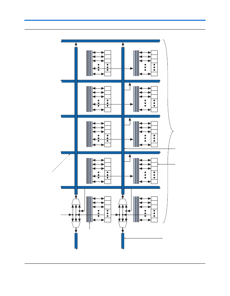
Figure 2–9
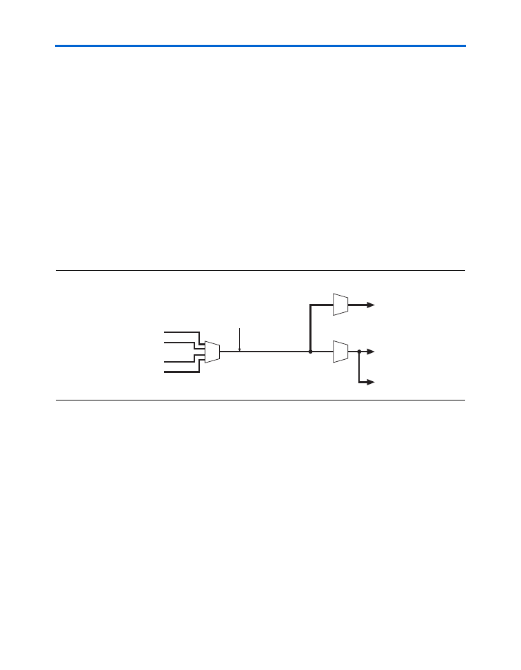
shows R4 interconnect connections from an LAB. R4
interconnects can drive and be driven by M4K memory blocks, PLLs, and
row IOEs. For LAB interfacing, a primary LAB or LAB neighbor can drive
a given R4 interconnect. For R4 interconnects that drive to the right, the
primary LAB and right neighbor can drive on to the interconnect. For R4
interconnects that drive to the left, the primary LAB and its left neighbor
can drive on to the interconnect. R4 interconnects can drive other R4
interconnects to extend the range of LABs they can drive. R4
interconnects can also drive C4 interconnects for connections from one
row to another.
FPGA_cyc-html.html
2–14
Altera
Corporation
Preliminary
February 2005
Cyclone Device Handbook, Volume 1
Figure 2–9. R4 Interconnect Connections
Notes to
Figure 2–9
:
(1)
C4 interconnects can drive R4 interconnects.
(2)
This pattern is repeated for every LAB in the LAB row.
The column interconnect operates similarly to the row interconnect. Each
column of LABs is served by a dedicated column interconnect, which
vertically routes signals to and from LABs, M4K memory blocks, and row
and column IOEs. These column resources include:
■
LUT chain interconnects within an LAB
■
Register chain interconnects within an LAB
■
C4 interconnects traversing a distance of four blocks in an up and
down direction
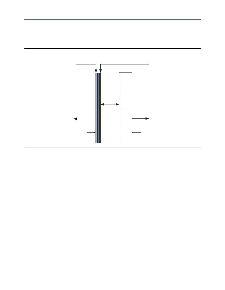
Cyclone devices include an enhanced interconnect structure within LABs
for routing LE output to LE input connections faster using LUT chain
connections and register chain connections. The LUT chain connection
allows the combinatorial output of an LE to directly drive the fast input
of the LE right below it, bypassing the local interconnect. These resources
can be used as a high-speed connection for wide fan-in functions from LE
1 to LE 10 in the same LAB. The register chain connection allows the
register output of one LE to connect directly to the register input of the
next LE in the LAB for fast shift registers. The Quartus II Compiler
automatically takes advantage of these resources to improve utilization
and performance.
Figure 2–10
shows the LUT chain and register chain
interconnects.
Primary
LAB (2)
R4 Interconnect
Driving Left
Adjacent LAB can
Drive onto Another
LAB's R4 Interconnect
C4 Column Interconnects (1)
R4 Interconnect
Driving Right
LAB
Neighbor
LAB
Neighbor
FPGA_cyc-html.html
Altera Corporation
2–15
February 2005
Preliminary
MultiTrack Interconnect
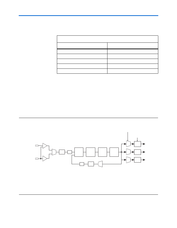
Figure 2–10. LUT Chain & Register Chain Interconnects
The C4 interconnects span four LABs or M4K blocks up or down from a
source LAB. Every LAB has its own set of C4 interconnects to drive either
up or down.
Figure 2–11
shows the C4 interconnect connections from an
LAB in a column. The C4 interconnects can drive and be driven by all
types of architecture blocks, including PLLs, M4K memory blocks, and
column and row IOEs. For LAB interconnection, a primary LAB or its
LAB neighbor can drive a given C4 interconnect. C4 interconnects can
drive each other to extend their range as well as drive row interconnects
for column-to-column connections.
LE 1
LE 2
LE 3
LE 4
LE 5
LE 6
LE 7
LE 8
LE 9
LE 10
LUT Chain
Routing to
Adjacent LE
Local
Interconnect
Register Chain
Routing to Adjacent
LE's Register Input
Local Interconnect
Routing Among LEs
in the LAB
FPGA_cyc-html.html
2–16
Altera
Corporation
Preliminary
February 2005
Cyclone Device Handbook, Volume 1
Figure 2–11. C4 Interconnect Connections
Note (1)
Note to
Figure 2–11
:
(1)
Each C4 interconnect can drive either up or down four rows.
C4 Interconnect
Drives Local and R4
Interconnects
Up to Four Rows
Adjacent LAB can
drive onto neighboring
LAB's C4 interconnect
C4 Interconnect
Driving Up
C4 Interconnect
Driving Down
LAB
Row
Interconnect
Local
Interconnect
FPGA_cyc-html.html
Altera Corporation
2–17
February 2005
Preliminary
MultiTrack Interconnect
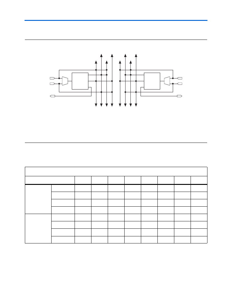
All embedded blocks communicate with the logic array similar to LAB-
to-LAB interfaces. Each block (i.e., M4K memory or PLL) connects to row
and column interconnects and has local interconnect regions driven by
row and column interconnects. These blocks also have direct link
interconnects for fast connections to and from a neighboring LAB.
Table 2–2
shows the Cyclone device's routing scheme.
Table 2–2. Cyclone Device Routing Scheme
Source
Destination
LUT Chain
Re
gister Cha
in
Local Inte
rconn
ect
Direct L
ink
Interconnect
R4
In
terconnect
C4 Interconnect
LE
M4
K RAM Bloc
k
PLL
Col
u
mn IO
E
Ro
w I
O
E
LUT Chain
v
Register Chain
v
Local Interconnect
v
v
v
v
v
Direct Link
Interconnect
v
R4 Interconnect
v
v
v
C4 Interconnect
v
v
v
LE
v
v
v
v
v
v
M4K RAM Block
v
v
v
v
PLL
v
v
v
Column IOE
v
Row IOE
v
v
v
FPGA_cyc-html.html
2–18
Altera
Corporation
Preliminary
February 2005
Cyclone Device Handbook, Volume 1
Embedded
Memory
The Cyclone embedded memory consists of columns of M4K memory
blocks. EP1C3 and EP1C6 devices have one column of M4K blocks, while
EP1C12 and EP1C20 devices have two columns (see
Table 1–1 on
page 1–2
for total RAM bits per density). Each M4K block can implement
various types of memory with or without parity, including true dual-port,
simple dual-port, and single-port RAM, ROM, and FIFO buffers. The
M4K blocks support the following features:
■
4,608 RAM bits
■
200 MHz performance
■
True dual-port memory
■
Simple dual-port memory
■
Single-port memory
■
Byte enable
■
Parity bits
■
Shift register
■
FIFO buffer
■
ROM
■
Mixed clock mode
1
Violating the setup or hold time on the address registers could corrupt the
memory contents. This applies to both read and write operations.
Memory Modes
The M4K memory blocks include input registers that synchronize writes
and output registers to pipeline designs and improve system
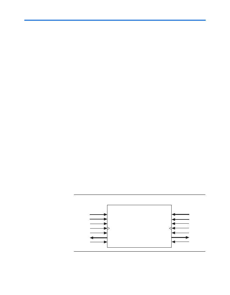
performance. M4K blocks offer a true dual-port mode to support any
combination of two-port operations: two reads, two writes, or one read
and one write at two different clock frequencies.
Figure 2–12
shows true
dual-port memory.
Figure 2–12. True Dual-Port Memory Configuration
data
A
[ ]
address
A
[ ]
wren
A
clock
A
clocken
A
q
A
[ ]
aclr
A
data
B
[ ]
address
B
[ ]
wren
B
clock
B
clocken
B
q
B
[ ]
aclr
B
A
B
FPGA_cyc-html.html
Altera Corporation
2–19
February 2005
Preliminary
Embedded Memory
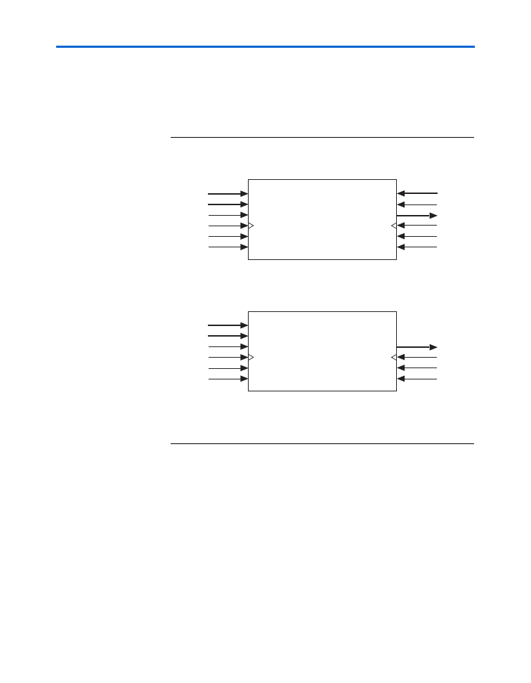
In addition to true dual-port memory, the M4K memory blocks support
simple dual-port and single-port RAM. Simple dual-port memory
supports a simultaneous read and write. Single-port memory supports
non-simultaneous reads and writes.
Figure 2–13
shows these different
M4K RAM memory port configurations.
Figure 2–13. Simple Dual-Port & Single-Port Memory Configurations
Note to
Figure 2–13
:
(1)
Two single-port memory blocks can be implemented in a single M4K block as long
as each of the two independent block sizes is equal to or less than half of the M4K
block size.
The memory blocks also enable mixed-width data ports for reading and
writing to the RAM ports in dual-port RAM configuration. For example,
the memory block can be written in
×
1 mode at port A and read out in
×
16
mode from port B.
The Cyclone memory architecture can implement fully synchronous
RAM by registering both the input and output signals to the M4K RAM
block. All M4K memory block inputs are registered, providing
synchronous write cycles. In synchronous operation, the memory block
generates its own self-timed strobe write enable (
wren
) signal derived
from a global clock. In contrast, a circuit using asynchronous RAM must
generate the RAM
wren
signal while ensuring its data and address
signals meet setup and hold time specifications relative to the
wren
data[ ]
wraddress[ ]
wren
inclock
inclocken
inaclr
rdaddress[ ]
rden
q[ ]
outclock
outclocken
outaclr
data[ ]
address[ ]
wren
inclock
inclocken
inaclr
q[ ]
outclock
outclocken
outaclr
Single-Port Memory
(1)
Simple Dual-Port Memory
FPGA_cyc-html.html

2–20
Altera
Corporation
Preliminary
February 2005
Cyclone Device Handbook, Volume 1
signal. The output registers can be bypassed. Pseudo-asynchronous
reading is possible in the simple dual-port mode of M4K blocks by
clocking the read enable and read address registers on the negative clock
edge and bypassing the output registers.
When configured as RAM or ROM, you can use an initialization file to
pre-load the memory contents.
Two single-port memory blocks can be implemented in a single M4K
block as long as each of the two independent block sizes is equal to or less
than half of the M4K block size.
The Quartus II software automatically implements larger memory by
combining multiple M4K memory blocks. For example, two 256
×
16-bit
RAM blocks can be combined to form a 256
×
32-bit RAM block. Memory
performance does not degrade for memory blocks using the maximum
number of words allowed. Logical memory blocks using less than the
maximum number of words use physical blocks in parallel, eliminating
any external control logic that would increase delays. To create a larger
high-speed memory block, the Quartus II software automatically
combines memory blocks with LE control logic.
Parity Bit Support
The M4K blocks support a parity bit for each byte. The parity bit, along
with internal LE logic, can implement parity checking for error detection
to ensure data integrity. You can also use parity-size data words to store
user-specified control bits. Byte enables are also available for data input
masking during write operations.
Shift Register Support
You can configure M4K memory blocks to implement shift registers for
DSP applications such as pseudo-random number generators, multi-
channel filtering, auto-correlation, and cross-correlation functions. These
and other DSP applications require local data storage, traditionally
implemented with standard flip-flops, which can quickly consume many
logic cells and routing resources for large shift registers. A more efficient
alternative is to use embedded memory as a shift register block, which
saves logic cell and routing resources and provides a more efficient
implementation with the dedicated circuitry.
The size of a
w
×
m
×
n
shift register is determined by the input data width
(
w
), the length of the taps (
m
), and the number of taps (
n
). The size of a
w
×
m
×
n
shift register must be less than or equal to the maximum number
of memory bits in the M4K block (4,608 bits). The total number of shift
FPGA_cyc-html.html
Altera Corporation
2–21
February 2005
Preliminary
Embedded Memory
register outputs (number of taps
n
×
width
w
) must be less than the
maximum data width of the M4K RAM block (
×
36). To create larger shift
registers, multiple memory blocks are cascaded together.
Data is written into each address location at the falling edge of the clock
and read from the address at the rising edge of the clock. The shift register
mode logic automatically controls the positive and negative edge
clocking to shift the data in one clock cycle.
Figure 2–14
shows the M4K
memory block in the shift register mode.
Figure 2–14. Shift Register Memory Configuration
Memory Configuration Sizes
The memory address depths and output widths can be configured as
4,096
×
1, 2,048
×
2, 1,024
×
4, 512
×
8 (or 512
×
9 bits), 256
×
16 (or 256
×
18
bits), and 128
×
32 (or 128
×
36 bits). The 128
×
32- or 36-bit configuration
m
-Bit Shift Register
w
w
m
-Bit Shift Register
m
-Bit Shift Register
m
-Bit Shift Register
w
w
w
w
w
w
w
×
m
×
n
Shift Register
n Number
of Taps
FPGA_cyc-html.html
2–22
Altera
Corporation
Preliminary
February 2005
Cyclone Device Handbook, Volume 1
is not available in the true dual-port mode. Mixed-width configurations
are also possible, allowing different read and write widths.
Tables 2–3
and
2–4
summarize the possible M4K RAM block configurations.
When the M4K RAM block is configured as a shift register block, you can
create a shift register up to 4,608 bits (
w
×
m
×
n
).
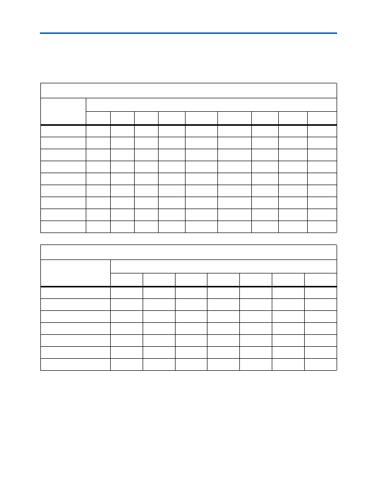
Table 2–3. M4K RAM Block Configurations (Simple Dual-Port)
Read Port
Write Port
4K
×
1
2K
×
2
1K
×
4
512
×
8
256
×
16
128
×
32
512
×
9 256
×
18 128
×
36
4K
×
1
v
v
v
v
v
v
2K
×
2
v
v
v
v
v
v
1K
×
4
v
v
v
v
v
v
512
×
8
v
v
v
v
v
v
256
×
16
v
v
v
v
v
v
128
×
32
v
v
v
v
v
v
512
×
9
v
v
v
256
×
18
v
v
v
128
×
36
v
v
v
Table 2–4. M4K RAM Block Configurations (True Dual-Port)
Port A
Port B
4K
×
1
2K
×
2
1K
×
4
512
×
8
256
×
16
512
×
9
256
×
18
4K
×
1
v
v
v
v
v
2K
×
2
v
v
v
v
v
1K
×
4
v
v
v
v
v
512
×
8
v
v
v
v
v
256
×
16
v
v
v
v
v
512
×
9
v
v
256
×
18
v
v
FPGA_cyc-html.html
Altera Corporation
2–23
February 2005
Preliminary
Embedded Memory
Byte Enables
M4K blocks support byte writes when the write port has a data width of
16, 18, 32, or 36 bits. The byte enables allow the input data to be masked
so the device can write to specific bytes. The unwritten bytes retain the
previous written value.
Table 2–5
summarizes the byte selection.
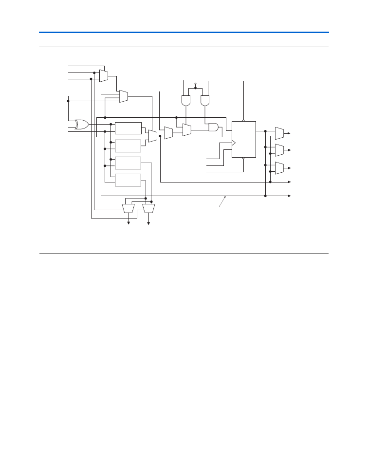
Control Signals & M4K Interface
The M4K blocks allow for different clocks on their inputs and outputs.
Either of the two clocks feeding the block can clock M4K block registers
(
renwe
, address, byte enable,
datain
, and output registers). Only the
output register can be bypassed. The six
labclk
signals or local
interconnects can drive the control signals for the A and B ports of the
M4K block. LEs can also control the
clock_a
,
clock_b
,
renwe_a
,
renwe_b
,
clr_a
,
clr_b
,
clocken_a
, and
clocken_b
signals, as
shown in
Figure 2–15
.
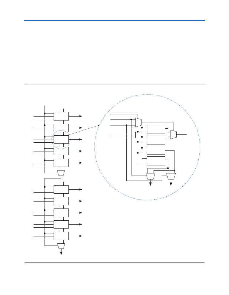
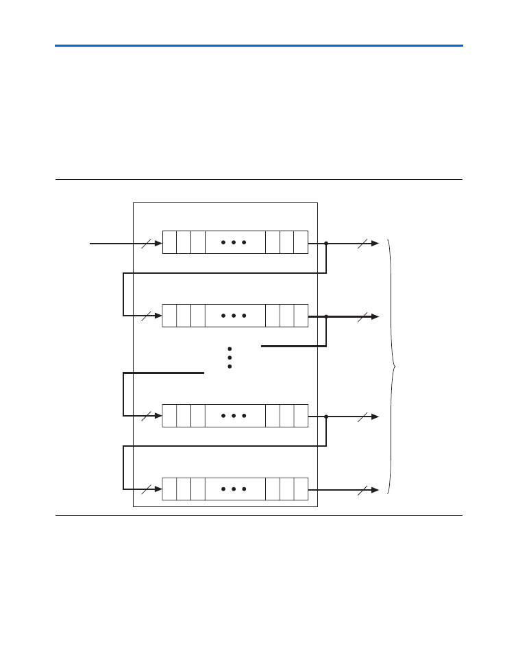
The R4, C4, and direct link interconnects from adjacent LABs drive the
M4K block local interconnect. The M4K blocks can communicate with
LABs on either the left or right side through these row resources or with
LAB columns on either the right or left with the column resources. Up to
10 direct link input connections to the M4K block are possible from the
left adjacent LABs and another 10 possible from the right adjacent LAB.
M4K block outputs can also connect to left and right LABs through 10
direct link interconnects each.
Figure 2–16
shows the M4K block to logic
array interface.
Table 2–5. Byte Enable for M4K Blocks
Notes (1)
,
(2)
byteena[3..0]
datain
×
18
datain
×
36
[0] = 1
[8..0]
[8..0]
[1] = 1
[17..9]
[17..9]
[2] = 1
–
[26..18]
[3] = 1
–
[35..27]
Notes to
Table 2–5
:
(1)
Any combination of byte enables is possible.
(2)
Byte enables can be used in the same manner with 8-bit words, i.e., in
×
16 and
×
32
modes.
FPGA_cyc-html.html
2–24
Altera
Corporation
Preliminary
February 2005
Cyclone Device Handbook, Volume 1
Figure 2–15. M4K RAM Block Control Signals
Figure 2–16. M4K RAM Block LAB Row Interface
clocken_a
renwe_a
clock_a
alcr_a
alcr_b
renwe_b
Dedicated
LAB Row
Clocks
Local
Interconnect
Local
Interconnect
Local
Interconnect
Local
Interconnect
Local
Interconnect
clocken_b
clock_b
6
Local
Interconnect
Local
Interconnect
Local
Interconnect
Local
Interconnect
Local
Interconnect
dataout
M4K RAM
Block
datain
address
10
Direct link
interconnect
from adjacent LAB
Direct link
interconnect
to adjacent LAB
Direct link
interconnect
from adjacent LAB
Direct link
interconnect
to adjacent LAB
M4K RAM Block Local
Interconnect Region
C4 Interconnects
R4 Interconnects
LAB Row Clocks
Clocks
Byte enable
Control
Signals
6
FPGA_cyc-html.html
Altera Corporation
2–25
February 2005
Preliminary
Embedded Memory
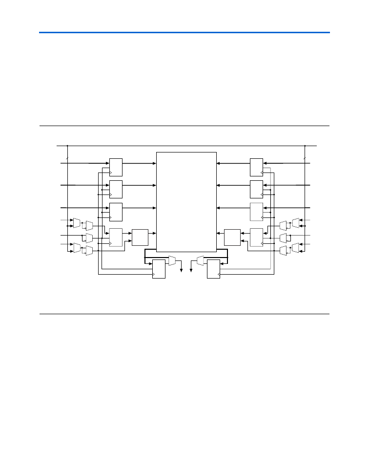
Independent Clock Mode
The M4K memory blocks implement independent clock mode for true
dual-port memory. In this mode, a separate clock is available for each port
(ports A and B). Clock A controls all registers on the port A side, while
clock B controls all registers on the port B side. Each port, A and B, also
supports independent clock enables and asynchronous clear signals for
port A and B registers.
Figure 2–17
shows an M4K memory block in
independent clock mode.
Figure 2–17. Independent Clock Mode
Notes (1)
,
(2)
Notes to
Figure 2–17
:
(1)
All registers shown have asynchronous clear ports.
(2)
Violating the setup or hold time on the address registers could corrupt the memory contents. This applies to both
read and write operations.
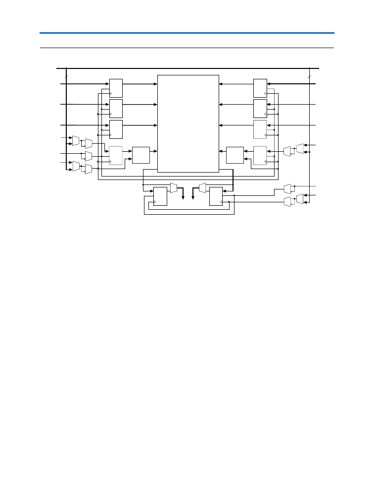
Input/Output Clock Mode
Input/output clock mode can be implemented for both the true and
simple dual-port memory modes. On each of the two ports, A or B, one
clock controls all registers for inputs into the memory block: data input,
wren
, and address. The other clock controls the block's data output
registers. Each memory block port, A or B, also supports independent
clock enables and asynchronous clear signals for input and output
registers.
Figures 2–18
and
2–19
show the memory block in input/output
clock mode.
6
D
ENA
Q
D
ENA
Q
D
ENA
Q
data
A
[ ]
address
A
[ ]
Memory Block
256 ´ 16 (2)
512 ´ 8
1,024 ´ 4
2,048 ´ 2
4,096 ´ 1
Data In
Address A
Write/Read
Enable
Data Out
Data In
Address B
Write/Read
Enable
Data Out
clken
A
clock
A
D
ENA
Q
wren
A
6 LAB Row Clocks
q
A
[ ]
6
data
B
[ ]
address
B
[ ]
clken
B
clock
B
wren
B
q
B
[ ]
ENA
A
B
ENA
D
Q
D
ENA
Q
byteena
A
[ ]
Byte Enable A
Byte Enable B
byteena
B
[ ]
ENA
D
Q
ENA
D
Q
ENA
D
Q
D
Q
Write
Pulse
Generator
Write
Pulse
Generator
FPGA_cyc-html.html
2–26
Altera
Corporation
Preliminary
February 2005
Cyclone Device Handbook, Volume 1
Figure 2–18. Input/Output Clock Mode in True Dual-Port Mode
Note (1)
,
(2)
Notes to
Figure 2–18
:
(1)
All registers shown have asynchronous clear ports.
(2)
Violating the setup or hold time on the address registers could corrupt the memory contents. This applies to both
read and write operations.
6
D
ENA
Q
D
ENA
Q
D
ENA
Q
data
A
[ ]
address
A
[ ]
Memory Block
256
×
16
(2)
512
×
8
1,024
×
4
2,048
×
2
4,096
×
1
Data In
Address A
Write/Read
Enable
Data Out
Data In
Address B
Write/Read
Enable
Data Out
clken
A
clock
A
D
ENA
Q
wren
A
6 LAB Row Clocks
q
A
[ ]
6
data
B
[ ]
address
B
[ ]
clken
B
clock
B
wren
B
q
B
[ ]
ENA
A
B
ENA
D
Q
ENA
D
Q
ENA
D
Q
D
Q
D
ENA
Q
byteena
A
[ ]
Byte Enable A
Byte Enable B
byteena
B
[ ]
ENA
D
Q
Write
Pulse
Generator
Write
Pulse
Generator
FPGA_cyc-html.html
Altera Corporation
2–27
February 2005
Preliminary
Embedded Memory
Figure 2–19. Input/Output Clock Mode in Simple Dual-Port Mode
Notes (1)
,
(2)
Notes to
Figure 2–19
:
(1)
All registers shown except the rden register have asynchronous clear ports.
(2)
Violating the setup or hold time on the address registers could corrupt the memory contents. This applies to both
read and write operations.
6
D
ENA
Q
D
ENA
Q
D
ENA
Q
D
ENA
Q
D
ENA
Q
data[ ]
D
ENA
Q
wraddress[ ]
address[ ]
Memory Block
256 ´ 16
512 ´ 8
1,024 ´ 4
2,048 ´ 2
4,096 ´ 1
Data In
Read Address
Write Address
Write Enable
Read Enable
Data Out
outclken
inclken
inclock
outclock
wren
rden
6 LAB Row
Clocks
To MultiTrack
Interconnect
D
ENA
Q
byteena[ ]
Byte Enable
Write
Pulse
Generator
FPGA_cyc-html.html
2–28
Altera
Corporation
Preliminary
February 2005
Cyclone Device Handbook, Volume 1
Read/Write Clock Mode
The M4K memory blocks implement read/write clock mode for simple
dual-port memory. You can use up to two clocks in this mode. The write
clock controls the block's data inputs,
wraddress
, and
wren
. The read
clock controls the data output,
rdaddress
, and
rden
. The memory
blocks support independent clock enables for each clock and
asynchronous clear signals for the read- and write-side registers.
Figure 2–20
shows a memory block in read/write clock mode.
Figure 2–20. Read/Write Clock Mode in Simple Dual-Port Mode
Notes (1)
,
(2)
Notes to
Figure 2–20
:
(1)
All registers shown except the rden register have asynchronous clear ports.
(2)
Violating the setup or hold time on the address registers could corrupt the memory contents. This applies to both
read and write operations.
6
D
ENA
Q
D
ENA
Q
D
ENA
Q
D
ENA
Q
D
ENA
Q
data[ ]
D
ENA
Q
wraddress[ ]
address[ ]
Memory Block
256
×
16
512
×
8
1,024
×
4
2,048
×
2
4,096
×
1
Data In
Read Address
Write Address
Write Enable
Read Enable
Data Out
rdclken
wrclken
wrclock
rdclock
wren
rden
6 LAB Row
Clocks
To MultiTrack
Interconnect
D
ENA
Q
byteena[ ]
Byte Enable
Write
Pulse
Generator
FPGA_cyc-html.html
Altera Corporation
2–29
February 2005
Preliminary
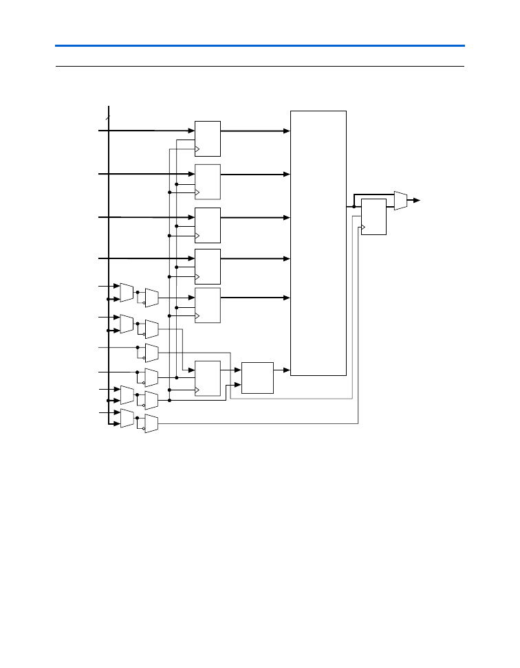
Global Clock Network & Phase-Locked Loops
Single-Port Mode
The M4K memory blocks also support single-port mode, used when
simultaneous reads and writes are not required. See
Figure 2–21
. A single
M4K memory block can support up to two single-port mode RAM blocks
if each RAM block is less than or equal to 2K bits in size.
Figure 2–21. Single-Port Mode
Note (1)
Note to
Figure 2–21
:
(1)
Violating the setup or hold time on the address registers could corrupt the memory contents. This applies to both
read and write operations.
Global Clock
Network &
Phase-Locked
Loops
Cyclone devices provide a global clock network and up to two PLLs for a
complete clock management solution.
Global Clock Network
There are four dedicated clock pins (
CLK[3..0]
, two pins on the left side
and two pins on the right side) that drive the global clock network, as
shown in
Figure 2–22
. PLL outputs, logic array, and dual-purpose clock
(
DPCLK[7..0]
) pins can also drive the global clock network.
6
D
ENA
Q
D
ENA
Q
D
ENA
Q
D
ENA
Q
data[ ]
address[ ]
RAM/ROM
256
×
16
512
×
8
1,024
×
4
2,048
×
2
4,096
×
1
Data In
Address
Write Enable
Data Out
outclken
inclken
inclock
outclock
Write
Pulse
Generator
wren
6 LAB Row
Clocks
To MultiTrack
Interconnect
FPGA_cyc-html.html
2–30
Altera
Corporation
Preliminary
February 2005
Cyclone Device Handbook, Volume 1
The eight global clock lines in the global clock network drive throughout
the entire device. The global clock network can provide clocks for all
resources within the device
⎯
IOEs, LEs, and memory blocks. The global
clock lines can also be used for control signals, such as clock enables and
synchronous or asynchronous clears fed from the external pin, or DQS
signals for DDR SDRAM or FCRAM interfaces. Internal logic can also
drive the global clock network for internally generated global clocks and
asynchronous clears, clock enables, or other control signals with large
fanout.
Figure 2–22
shows the various sources that drive the global clock
network.
Figure 2–22. Global Clock Generation
Note (1)
Notes to
Figure 2–22
:
(1)
The EP1C3 device in the 100-pin TQFP package has five
DPCLK
pins (
DPCLK2
,
DPCLK3
,
DPCLK4
,
DPCLK6
, and
DPCLK7
).
(2)
EP1C3 devices only contain one PLL (PLL 1).
(3)
The EP1C3 device in the 100-pin TQFP package does not have dedicated clock pins
CLK1
and
CLK3
.
8
Global Clock
Network
PLL1
PLL2
(2)
CLK0
CLK1
(3)
CLK2
CLK3
(3)
DPCLK1
DPCLK0
DPCLK4
DPCLK5
DPCLK2
DPCLK3
DPCLK7
DPCLK6
2
2
From logic
array
From logic
array
4
4
4
4
Cyclone Device
FPGA_cyc-html.html
Altera Corporation
2–31
February 2005
Preliminary
Global Clock Network & Phase-Locked Loops
Dual-Purpose Clock Pins
Each Cyclone device except the EP1C3 device has eight dual-purpose
clock pins,
DPCLK[7..0]
(two on each I/O bank). EP1C3 devices have
five
DPCLK
pins in the 100-pin TQFP package. These dual-purpose pins
can connect to the global clock network (see
Figure 2–22
) for high-fanout
control signals such as clocks, asynchronous clears, presets, and clock
enables, or protocol control signals such as
TRDY
and
IRDY
for PCI, or
DQS signals for external memory interfaces.
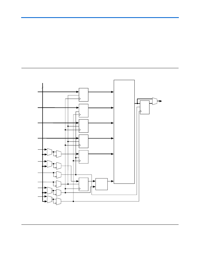
Combined Resources
Each Cyclone device contains eight distinct dedicated clocking resources.
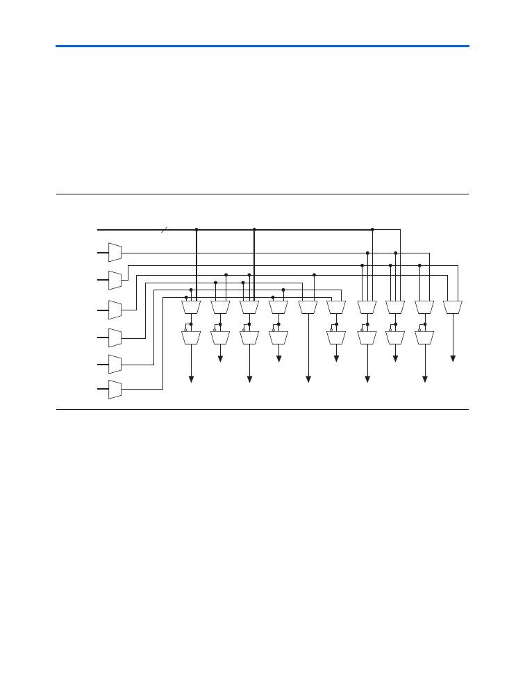
The device uses multiplexers with these clocks to form six-bit buses to
drive LAB row clocks, column IOE clocks, or row IOE clocks. See
Figure 2–23
. Another multiplexer at the LAB level selects two of the six
LAB row clocks to feed the LE registers within the LAB.
Figure 2–23. Global Clock Network Multiplexers
IOE clocks have row and column block regions. Six of the eight global
clock resources feed to these row and column regions.
Figure 2–24
shows
the I/O clock regions.
Clock [7..0]
Column I/O Region
IO_CLK]5..0]
LAB Row Clock [5..0]
Row I/O Region
IO_CLK[5..0]
Global Clocks [3..0]
PLL Outputs [3..0]
Dual-Purpose Clocks [7..0]
Global Clock
Network
Core Logic [7..0]
FPGA_cyc-html.html
2–32
Altera
Corporation
Preliminary
February 2005
Cyclone Device Handbook, Volume 1
Figure 2–24. I/O Clock Regions
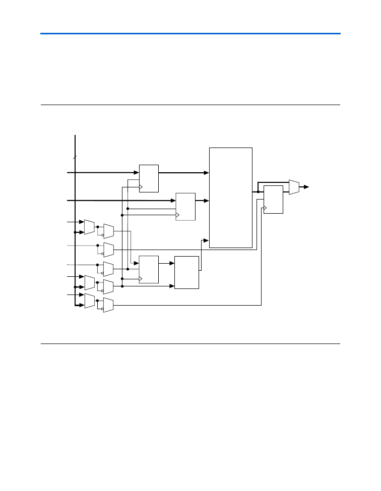
PLLs
Cyclone PLLs provide general-purpose clocking with clock
multiplication and phase shifting as well as outputs for differential I/O
support. Cyclone devices contain two PLLs, except for the EP1C3 device,
which contains one PLL.
Column I/O Clock Region
IO_CLK[5..0]
Column I/O Clock Region
IO_CLK[5..0]
6
6
I/O Clock Regions
I/O Clock Regions
8
Global Clock
Network
Row
I/O Regions
Cyclone Logic Array
6
6
LAB Row Clocks
labclk[5..0]
LAB Row Clocks
labclk[5..0]
LAB Row Clocks
labclk[5..0]
LAB Row Clocks
labclk[5..0]
LAB Row Clocks
labclk[5..0]
LAB Row Clocks
labclk[5..0]
6
6
6
6
FPGA_cyc-html.html
Altera Corporation
2–33
February 2005
Preliminary
Global Clock Network & Phase-Locked Loops
Table 2–6
shows the PLL features in Cyclone devices.
Figure 2–25
shows
a Cyclone PLL.
Figure 2–25. Cyclone PLL
Note (1)
Notes to
Figure 2–25
:
(1)
The EP1C3 device in the 100-pin TQFP package does not support external outputs or LVDS inputs. The EP1C6
device in the 144-pin TQFP package does not support external output from PLL2.
(2)
LVDS input is supported via the secondary function of the dedicated clock pins. For PLL 1, the
CLK0
pin’s secondary
function is
LVDSCLK1p
and the
CLK1
pin’s secondary function is
LVDSCLK1n
. For PLL 2, the
CLK2
pin’s secondary
function is
LVDSCLK2p
and the
CLK3
pin’s secondary function is
LVDSCLK2n
.
(3)
PFD: phase frequency detector.
Table 2–6. Cyclone PLL Features
Feature
PLL Support
Clock multiplication and division
m
/(
n
×
post-scale counter)
(1)
Phase shift
Down to 125-ps increments
(2)
,
(3)
Programmable duty cycle
Yes
Number of internal clock outputs
2
Number of external clock outputs
One differential or one single-ended
(4)
Notes to
Table 2–6
:
(1)
The
m
counter ranges from 2 to 32. The
n
counter and the post-scale counters
range from 1 to 32.
(2)
The smallest phase shift is determined by the voltage-controlled oscillator (VCO)
period divided by 8.
(3)
For degree increments, Cyclone devices can shift all output frequencies in
increments of 45°. Smaller degree increments are possible depending on the
frequency and divide parameters.
(4)
The EP1C3 device in the 100-pin TQFP package does not support external clock
output. The EP1C6 device in the 144-pin TQFP package does not support external
clock output from PLL2.
Charge
Pump
VCO
PFD
(3)
Loop
Filter
CLK0 or
LVDSCLK1p
(2)
CLK1 or
LVDSCLK1n
(2)
÷
n
÷
m
∆
t
∆
t
Global clock
Global clock
I/O buffer
÷g0
÷g1
÷e
VCO Phase Selection
Selectable at Each PLL
Output Port
Post-Scale
Counters
FPGA_cyc-html.html
2–34
Altera
Corporation
Preliminary
February 2005
Cyclone Device Handbook, Volume 1
Figure 2–26
shows the PLL global clock connections.
Figure 2–26. Cyclone PLL Global Clock Connections
Notes to
Figure 2–26
:
(1)
PLL 1 supports one single-ended or LVDS input via pins
CLK0
and
CLK1
.
(2)
PLL2 supports one single-ended or LVDS input via pins
CLK2
and
CLK3
.
(3)
PLL1_OUT
and
PLL2_OUT
support single-ended or LVDS output. If external output is not required, these pins are
available as regular user I/O pins.
(4)
The EP1C3 device in the 100-pin TQFP package does not support external clock output. The EP1C6 device in the
144-pin TQFP package does not support external clock output from PLL2.
Table 2–7
shows the global clock network sources available in Cyclone
devices.
CLK0
CLK1
(1)
PLL1
PLL2
g0
g1
e
g0
g1
e
PLL1_OUT
(3), (4)
CLK2
CLK3
(2)
PLL2_OUT
(3), (4)
G0
G2
G1
G3
G4
G6
G5
G7
Table 2–7. Global Clock Network Sources (Part 1 of 2)
Source
GCLK0
GCLK1
GCLK2
GCLK3
GCLK4
GCLK5
GCLK6
GCLK7
PLL Counter
Output
PLL1 G0
v
v
PLL1 G1
v
v
PLL2 G0
(1)
v
v
PLL2 G1
(1)
v
v
Dedicated
Clock Input
Pins
CLK0
v
v
CLK1
(2)
v
v
CLK2
v
v
CLK3
(2)
v
v
FPGA_cyc-html.html
Altera Corporation
2–35
February 2005
Preliminary
Global Clock Network & Phase-Locked Loops
Clock Multiplication & Division
Cyclone PLLs provide clock synthesis for PLL output ports using
m
/(
n
×
post scale counter) scaling factors. The input clock is divided by
a pre-scale divider,
n
, and is then multiplied by the
m
feedback factor. The
control loop drives the VCO to match f
IN
×
(
m
/
n
). Each output port has
a unique post-scale counter to divide down the high-frequency VCO. For
multiple PLL outputs with different frequencies, the VCO is set to the
least-common multiple of the output frequencies that meets its frequency
specifications. Then, the post-scale dividers scale down the output
frequency for each output port. For example, if the output frequencies
required from one PLL are 33 and 66 MHz, the VCO is set to 330 MHz (the
least-common multiple in the VCO's range).
Each PLL has one pre-scale divider,
n
, that can range in value from 1 to
32. Each PLL also has one multiply divider,
m
, that can range in value
from 2 to 32. Global clock outputs have two post scale G dividers for
global clock outputs, and external clock outputs have an E divider for
external clock output, both ranging from 1 to 32. The Quartus II software
automatically chooses the appropriate scaling factors according to the
input frequency, multiplication, and division values entered.
Dual-Purpose
Clock Pins
DPCLK0
(3)
v
DPCLK1
(3)
v
DPCLK2
v
DPCLK3
v
DPCLK4
v
DPCLK5
(3)
v
DPCLK6
v
DPCLK7
v
Notes to
Table 2–7
:
(1)
EP1C3 devices only have one PLL (PLL 1).
(2)
EP1C3 devices in the 100-pin TQFP package do not have dedicated clock pins
CLK1
and
CLK3
.
(3)
EP1C3 devices in the 100-pin TQFP package do not have the
DPCLK0
,
DPCLK1
, or
DPCLK5
pins.
Table 2–7. Global Clock Network Sources (Part 2 of 2)
Source
GCLK0
GCLK1
GCLK2
GCLK3
GCLK4
GCLK5
GCLK6
GCLK7
FPGA_cyc-html.html
2–36
Altera
Corporation
Preliminary
February 2005
Cyclone Device Handbook, Volume 1
External Clock Inputs
Each PLL supports single-ended or differential inputs for source-
synchronous receivers or for general-purpose use. The dedicated clock
pins (
CLK[3..0]
) feed the PLL inputs. These dual-purpose pins can also
act as LVDS input pins. See
Figure 2–25
.
Table 2–8
shows the I/O standards supported by PLL input and output
pins.
For more information on LVDS I/O support, see
“LVDS I/O Pins” on
page 2–54
.
External Clock Outputs
Each PLL supports one differential or one single-ended output for source-
synchronous transmitters or for general-purpose external clocks. If the
PLL does not use these
PLL_OUT
pins, the pins are available for use as
general-purpose I/O pins. The
PLL_OUT
pins support all I/O standards
shown in
Table 2–8
.
The external clock outputs do not have their own V
CC
and ground voltage
supplies. Therefore, to minimize jitter, do not place switching I/O pins
next to these output pins. The EP1C3 device in the 100-pin TQFP package
Table 2–8. PLL I/O Standards
I/O Standard
CLK Input
EXTCLK Output
3.3-V LVTTL/LVCMOS
v
v
2.5-V LVTTL/LVCMOS
v
v
1.8-V LVTTL/LVCMOS
v
v
1.5-V LVCMOS
v
v
3.3-V PCI
v
v
LVDS
v
v
SSTL-2 class I
v
v
SSTL-2 class II
v
v
SSTL-3 class I
v
v
SSTL-3 class II
v
v
Differential SSTL-2
v
FPGA_cyc-html.html

Altera Corporation
2–37
February 2005
Preliminary
Global Clock Network & Phase-Locked Loops
does not have dedicated clock output pins. The EP1C6 device in the
144-pin TQFP package only supports dedicated clock outputs from
PLL 1.
Clock Feedback
Cyclone PLLs have three modes for multiplication and/or phase shifting:
■
Zero delay buffer mode
⎯
The external clock output pin is phase-
aligned with the clock input pin for zero delay.
■
Normal mode
⎯
If the design uses an internal PLL clock output, the
normal mode compensates for the internal clock delay from the input
clock pin to the IOE registers. The external clock output pin is phase
shifted with respect to the clock input pin if connected in this mode.
You defines which internal clock output from the PLL should be
phase-aligned to compensate for internal clock delay.
■
No compensation mode
⎯
In this mode, the PLL will not compensate
for any clock networks.
Phase Shifting
Cyclone PLLs have an advanced clock shift capability that enables
programmable phase shifts. You can enter a phase shift (in degrees or
time units) for each PLL clock output port or for all outputs together in
one shift. You can perform phase shifting in time units with a resolution
range of 125 to 250 ps. The finest resolution equals one eighth of the VCO
period. The VCO period is a function of the frequency input and the
multiplication and division factors. Each clock output counter can choose
a different phase of the VCO period from up to eight taps. You can use this
clock output counter along with an initial setting on the post-scale
counter to achieve a phase-shift range for the entire period of the output
clock. The phase tap feedback to the m counter can shift all outputs to a
single phase. The Quartus II software automatically sets the phase taps
and counter settings according to the phase shift entered.
Lock Detect Signal
The lock output indicates that there is a stable clock output signal in
phase with the reference clock. Without any additional circuitry, the lock
signal may toggle as the PLL begins tracking the reference clock.
Therefore, you may need to gate the lock signal for use as a system-
control signal. For correct operation of the lock circuit below –20 C, f
IN/N
> 200 MHz.
FPGA_cyc-html.html

2–38
Altera
Corporation
Preliminary
February 2005
Cyclone Device Handbook, Volume 1
Programmable Duty Cycle
The programmable duty cycle allows PLLs to generate clock outputs with
a variable duty cycle. This feature is supported on each PLL post-scale
counter (g0, g1, e). The duty cycle setting is achieved by a low- and high-
time count setting for the post-scale dividers. The Quartus II software
uses the frequency input and the required multiply or divide rate to
determine the duty cycle choices.
Control Signals
There are three control signals for clearing and enabling PLLs and their
outputs. You can use these signals to control PLL resynchronization and
the ability to gate PLL output clocks for low-power applications.
The
pllenable
signal enables and disables PLLs. When the
pllenable
signal is low, the clock output ports are driven by ground and all the PLLs
go out of lock. When the
pllenable
signal goes high again, the PLLs
relock and resynchronize to the input clocks. An input pin or LE output
can drive the
pllenable
signal.
The
areset
signals are reset/resynchronization inputs for each PLL.
Cyclone devices can drive these input signals from input pins or from
LEs. When
areset
is driven high, the PLL counters will reset, clearing
the PLL output and placing the PLL out of lock. When driven low again,
the PLL will resynchronize to its input as it relocks.
The
pfdena
signals control the phase frequency detector (PFD) output
with a programmable gate. If you disable the PFD, the VCO will operate
at its last set value of control voltage and frequency with some drift, and
the system will continue running when the PLL goes out of lock or the
input clock disables. By maintaining the last locked frequency, the system
has time to store its current settings before shutting down. You can either
use their own control signal or gated locked status signals to trigger the
pfdena
signal.
f
For more information on Cyclone PLLs, see
Chapter 6, Using PLLs in
Cyclone Devices
.
FPGA_cyc-html.html

Altera Corporation
2–39
February 2005
Preliminary
I/O Structure
I/O Structure
IOEs support many features, including:
■
Differential and single-ended I/O standards
■
3.3-V, 64- and 32-bit, 66- and 33-MHz PCI compliance
■
Joint Test Action Group (JTAG) boundary-scan test (BST) support
■
Output drive strength control
■
Weak pull-up resistors during configuration
■
Slew-rate control
■
Tri-state buffers
■
Bus-hold circuitry
■
Programmable pull-up resistors in user mode
■
Programmable input and output delays
■
Open-drain outputs
■
DQ and DQS I/O pins
Cyclone device IOEs contain a bidirectional I/O buffer and three registers
for complete embedded bidirectional single data rate transfer.
Figure 2–27
shows the Cyclone IOE structure. The IOE contains one input
register, one output register, and one output enable register. You can use
the input registers for fast setup times and output registers for fast clock-
to-output times. Additionally, you can use the output enable (OE) register
for fast clock-to-output enable timing. The Quartus II software
automatically duplicates a single OE register that controls multiple
output or bidirectional pins. IOEs can be used as input, output, or
bidirectional pins.
FPGA_cyc-html.html
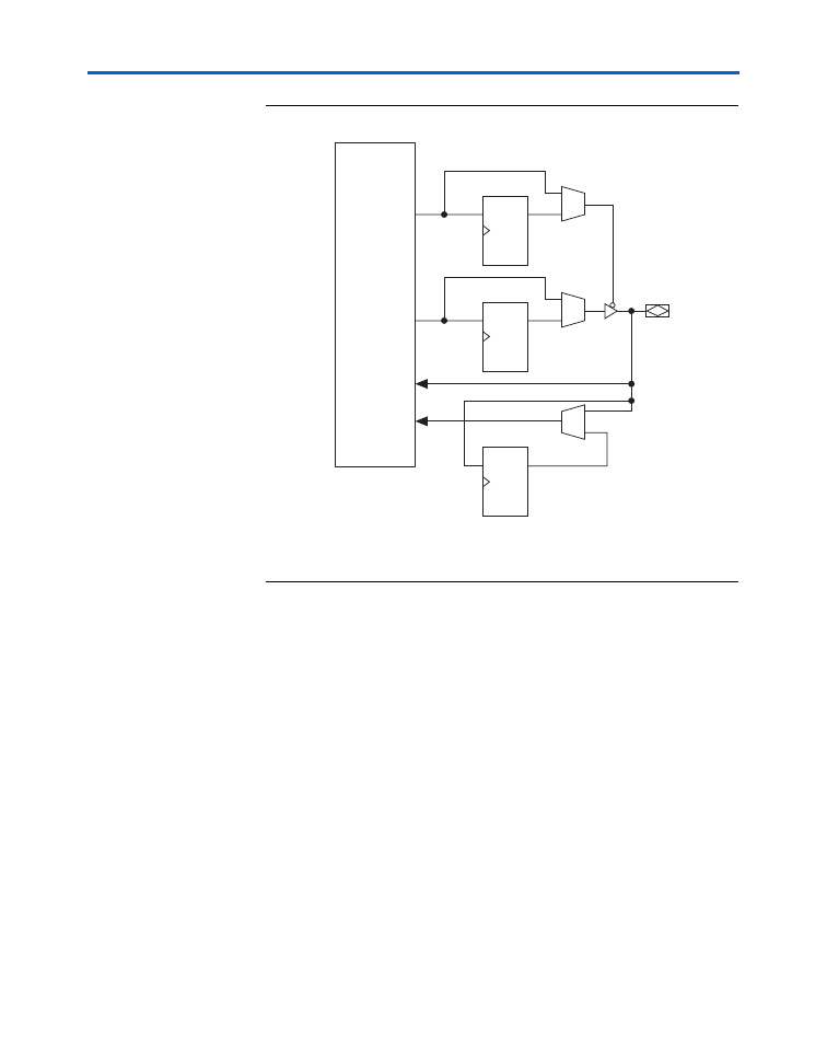
2–40
Altera
Corporation
Preliminary
February 2005
Cyclone Device Handbook, Volume 1
Figure 2–27. Cyclone IOE Structure
Note to
Figure 2–27
:
(1)
There are two paths available for combinatorial inputs to the logic array. Each path
contains a unique programmable delay chain.
The IOEs are located in I/O blocks around the periphery of the Cyclone
device. There are up to three IOEs per row I/O block and up to three IOEs
per column I/O block (column I/O blocks span two columns). The row
I/O blocks drive row, column, or direct link interconnects. The column
I/O blocks drive column interconnects.
Figure 2–28
shows how a row
I/O block connects to the logic array.
Figure 2–29
shows how a column
I/O block connects to the logic array.
Output Register
Output
Combinatorial
input
(1)
Input
OE Register
OE
Input Register
Logic Array
D
Q
D
Q
D
Q
FPGA_cyc-html.html
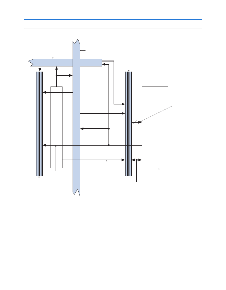
Altera Corporation
2–41
February 2005
Preliminary
I/O Structure
Figure 2–28. Row I/O Block Connection to the Interconnect
Notes to
Figure 2–28
:
(1)
The 21 data and control signals consist of three data out lines,
io_dataout[2..0]
, three output enables,
io_coe[2..0]
, three input clock enables,
io_cce_in[2..0]
, three output clock enables,
io_cce_out[2..0]
,
three clocks,
io_cclk[2..0]
, three asynchronous clear signals,
io_caclr[2..0]
, and three synchronous clear
signals,
io_csclr[2..0]
.
(2)
Each of the three IOEs in the row I/O block can have one
io_datain
input (combinatorial or registered) and one
comb_io_datain
(combinatorial) input.
21
R4 Interconnects
C4 Interconnects
I/O Block Local
Interconnect
21 Data and
Control Signals
from Logic Array (1)
io_datain[2..0] and
comb_io_datain[2..0]
(2)
io_clk[5:0]
Row I/O Block
Contains up to
Three IOEs
Direct Link
Interconnect
to Adjacent LAB
Direct Link
Interconnect
from Adjacent LAB
LAB Local
Interconnect
LAB
Row
I/O Block
FPGA_cyc-html.html
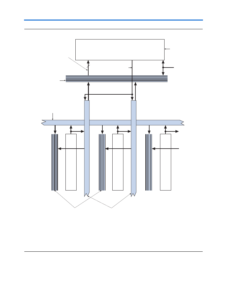
2–42
Altera
Corporation
Preliminary
February 2005
Cyclone Device Handbook, Volume 1
Figure 2–29. Column I/O Block Connection to the Interconnect
Notes to
Figure 2–29
:
(1)
The 21 data and control signals consist of three data out lines,
io_dataout[2..0]
, three output enables,
io_coe[2..0]
, three input clock enables,
io_cce_in[2..0]
, three output clock enables,
io_cce_out[2..0]
,
three clocks,
io_cclk[2..0]
, three asynchronous clear signals,
io_caclr[2..0]
, and three synchronous clear
signals,
io_csclr[2..0]
.
(2)
Each of the three IOEs in the column I/O block can have one
io_datain
input (combinatorial or registered) and
one
comb_io_datain
(combinatorial) input.
21 Data &
Control Signals
from Logic Array (1)
Column I/O
Block Contains
up to Three IOEs
I/O Block
Local Interconnect
IO_datain[2:0] &
comb_io_datain[2..0]
(2)
R4 Interconnects
LAB Local
Interconnect
C4 Interconnects
21
LAB
LAB
LAB
io_clk[5..0]
Column I/O Block
FPGA_cyc-html.html
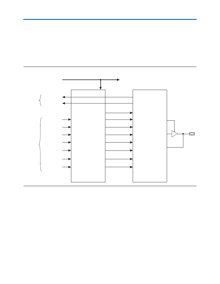
Altera Corporation
2–43
February 2005
Preliminary
I/O Structure
The pin's datain signals can drive the logic array. The logic array drives
the control and data signals, providing a flexible routing resource. The
row or column IOE clocks,
io_clk[5..0]
, provide a dedicated routing
resource for low-skew, high-speed clocks. The global clock network
generates the IOE clocks that feed the row or column I/O regions (see
“Global Clock Network & Phase-Locked Loops” on page 2–29
).
Figure 2–30
illustrates the signal paths through the I/O block.
Figure 2–30. Signal Path through the I/O Block
Each IOE contains its own control signal selection for the following
control signals:
oe
,
ce_in
,
ce_out
,
aclr
/
preset
,
sclr
/
preset
,
clk_in
, and
clk_out
.
Figure 2–31
illustrates the control signal
selection.
Row or Column
io_clk[5..0]
io_datain
comb_io_datain
io_dataout
io_coe
oe
ce_in
ce_out
io_cce_in
aclr/preset
io_cce_out
sclr
io_caclr
clk_in
io_cclk
clk_out
dataout
Data and
Control
Signal
Selection
IOE
To Logic
Array
From Logic
Array
To Other
IOEs
io_csclr
FPGA_cyc-html.html
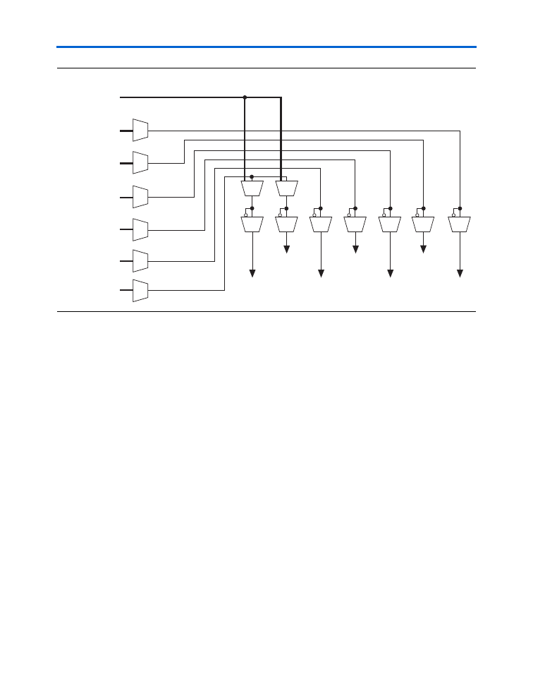
2–44
Altera
Corporation
Preliminary
February 2005
Cyclone Device Handbook, Volume 1
Figure 2–31. Control Signal Selection per IOE
In normal bidirectional operation, you can use the input register for input
data requiring fast setup times. The input register can have its own clock
input and clock enable separate from the OE and output registers. The
output register can be used for data requiring fast clock-to-output
performance. The OE register is available for fast clock-to-output enable
timing. The OE and output register share the same clock source and the
same clock enable source from the local interconnect in the associated
LAB, dedicated I/O clocks, or the column and row interconnects.
Figure 2–32
shows the IOE in bidirectional configuration.
clk_out
ce_in
clk_in
ce_out
aclr/preset
sclr/preset
Dedicated I/O
Clock [5..0]
Local
Interconnect
Local
Interconnect
Local
Interconnect
Local
Interconnect
Local
Interconnect
oe
io_coe
io_caclr
Local
Interconnect
io_csclr
io_cce_out
io_cce_in
io_cclk
FPGA_cyc-html.html
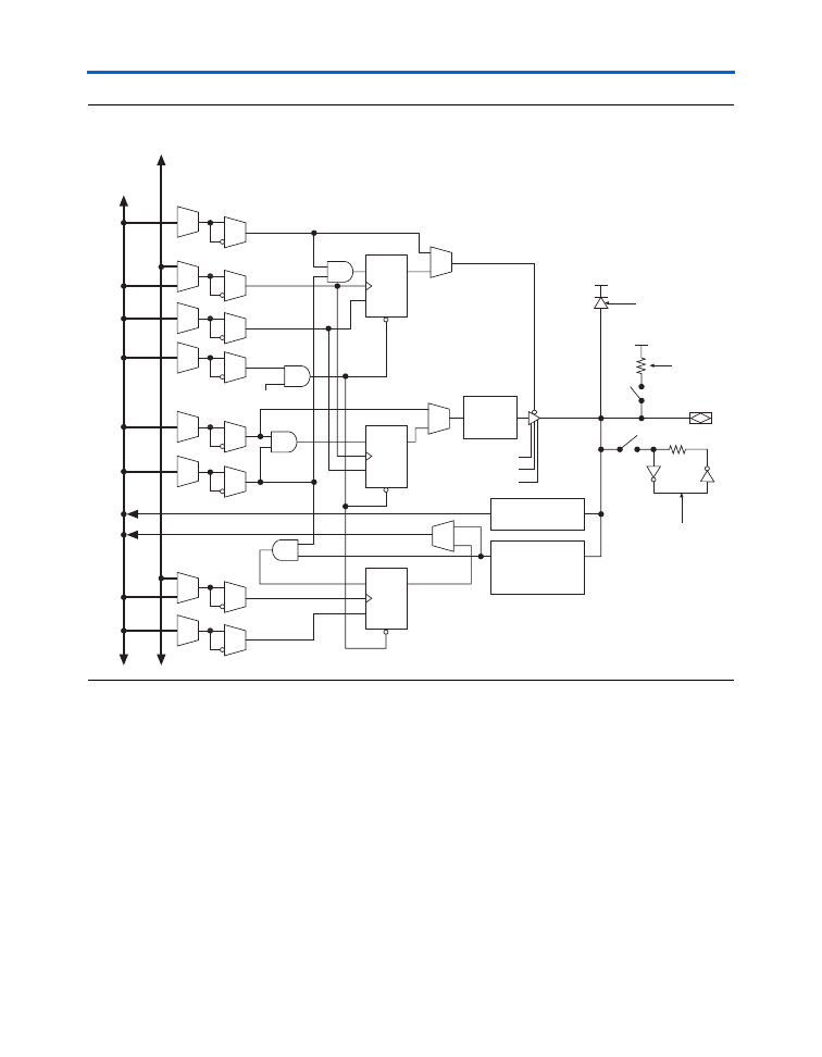
Altera Corporation
2–45
February 2005
Preliminary
I/O Structure
Figure 2–32. Cyclone IOE in Bidirectional I/O Configuration
The Cyclone device IOE includes programmable delays to ensure zero
hold times, minimize setup times, or increase clock to output times.
A path in which a pin directly drives a register may require a
programmable delay to ensure zero hold time, whereas a path in which a
pin drives a register through combinatorial logic may not require the
delay. Programmable delays decrease input-pin-to-logic-array and IOE
input register delays. The Quartus II Compiler can program these delays
Chip-Wide Reset
OE Register
V
CCIO
Optional
PCI Clamp
Column or Row
Interconect
ioe_clk[5..0]
Input Register
Input Pin to
Input Register Delay
or Input Pin to
Logic Array Delay
Input Pin to
Logic Array Delay
Drive Strength Control
Open-Drain Output
Slew Control
sclr/preset
OE
clkout
ce_out
aclr/prn
clkin
ce_in
Output
Pin Delay
Programmable
Pull-Up
Resistor
Bus Hold
PRN
CLRN
D
Q
Output Register
PRN
CLRN
D
Q
PRN
CLRN
D
Q
V
CCIO
comb_datain
data_in
ENA
ENA
ENA
FPGA_cyc-html.html
2–46
Altera
Corporation
Preliminary
February 2005
Cyclone Device Handbook, Volume 1
to automatically minimize setup time while providing a zero hold time.
Programmable delays can increase the register-to-pin delays for output
registers.
Table 2–9
shows the programmable delays for Cyclone devices.
There are two paths in the IOE for a combinatorial input to reach the logic
array. Each of the two paths can have a different delay. This allows you
adjust delays from the pin to internal LE registers that reside in two
different areas of the device. The designer sets the two combinatorial
input delays by selecting different delays for two different paths under
the
Decrease input delay to internal cells
logic option in the Quartus II
software. When the input signal requires two different delays for the
combinatorial input, the input register in the IOE is no longer available.
The IOE registers in Cyclone devices share the same source for clear or
preset. The designer can program preset or clear for each individual IOE.
The designer can also program the registers to power up high or low after
configuration is complete. If programmed to power up low, an
asynchronous clear can control the registers. If programmed to power up
high, an asynchronous preset can control the registers. This feature
prevents the inadvertent activation of another device's active-low input
upon power up. If one register in an IOE uses a preset or clear signal then
all registers in the IOE must use that same signal if they require preset or
clear. Additionally a synchronous reset signal is available to the designer
for the IOE registers.
External RAM Interfacing
Cyclone devices support DDR SDRAM and FCRAM interfaces at up to
133 MHz through dedicated circuitry.
DDR SDRAM & FCRAM
Cyclone devices have dedicated circuitry for interfacing with DDR
SDRAM. All I/O banks support DDR SDRAM and FCRAM I/O pins.
However, the configuration input pins in bank 1 must operate at 2.5 V
because the SSTL-2 V
CCIO
level is 2.5 V. Additionally, the configuration
Table 2–9. Cyclone Programmable Delay Chain
Programmable Delays
Quartus II Logic Option
Input pin to logic array delay
Decrease input delay to internal cells
Input pin to input register delay
Decrease input delay to input registers
Output pin delay
Increase delay to output pin
FPGA_cyc-html.html
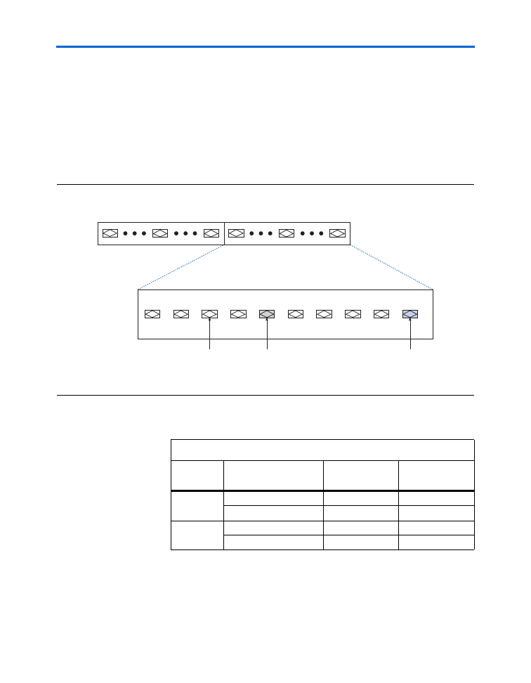
Altera Corporation
2–47
February 2005
Preliminary
I/O Structure
output pins (
nSTATUS
and
CONF_DONE
) and all the JTAG pins in I/O
bank 3 must operate at 2.5 V because the V
CCIO
level of SSTL-2 is 2.5 V.
I/O banks 1, 2, 3, and 4 support DQS signals with DQ bus modes of
×
8.
For
×
8 mode, there are up to eight groups of programmable DQS and DQ
pins, I/O banks 1, 2, 3, and 4 each have two groups in the 324-pin and
400-pin FineLine BGA packages. Each group consists of one DQS pin, a
set of eight DQ pins, and one DM pin (see
Figure 2–33
). Each DQS pin
drives the set of eight DQ pins within that group.
Figure 2–33. Cyclone Device DQ & DQS Groups in
×
8 Mode
Note (1)
Note to
Figure 2–33
:
(1)
Each DQ group consists of one DQS pin, eight DQ pins, and one DM pin.
Table 2–10
shows the number of DQ pin groups per device.
DQ Pins
DQS Pin
DM Pin
Top, Bottom, Left, or Right I/O Bank
Table 2–10. DQ Pin Groups (Part 1 of 2)
Device
Package
Number of
×
8 DQ
Pin Groups
Total DQ Pin
Count
EP1C3
100-pin TQFP
(1)
3
24
144-pin TQFP
4
32
EP1C4
324-pin FineLine BGA
8
64
400-pin FineLine BGA
8
64
FPGA_cyc-html.html
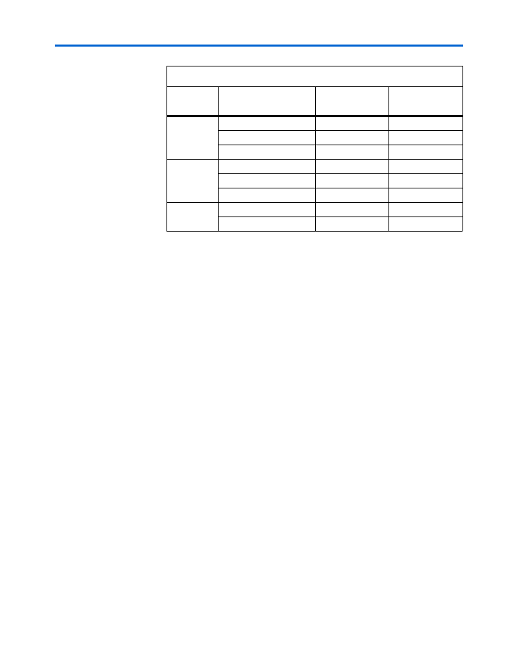
2–48
Altera
Corporation
Preliminary
February 2005
Cyclone Device Handbook, Volume 1
A programmable delay chain on each DQS pin allows for either a 90°
phase shift (for DDR SDRAM), or a 72° phase shift (for FCRAM) which
automatically center-aligns input DQS synchronization signals within the
data window of their corresponding DQ data signals. The phase-shifted
DQS signals drive the global clock network. This global DQS signal clocks
DQ signals on internal LE registers.
These DQS delay elements combine with the PLL’s clocking and phase
shift ability to provide a complete hardware solution for interfacing to
high-speed memory.
The clock phase shift allows the PLL to clock the DQ output enable and
output paths. The designer should use the following guidelines to meet
133 MHz performance for DDR SDRAM and FCRAM interfaces:
■
The DQS signal must be in the middle of the DQ group it clocks
■
Resynchronize the incoming data to the logic array clock using
successive LE registers or FIFO buffers
■
LE registers must be placed in the LAB adjacent to the DQ I/O pin
column it is fed by
Figure 2–34
illustrates DDR SDRAM and FCRAM interfacing from the
I/O through the dedicated circuitry to the logic array.
EP1C6
144-pin TQFP
4
32
240-pin PQFP
4
32
256-pin FineLine BGA
4
32
EP1C12
240-pin PQFP
4
32
256-pin FineLine BGA
4
32
324-pin FineLine BGA
8
64
EP1C20
324-pin FineLine BGA
8
64
400-pin FineLine BGA
8
64
Note to
Table 2–10
:
(1)
EP1C3 devices in the 100-pin TQFP package do not have any DQ pin groups in
I/O bank 1.
Table 2–10. DQ Pin Groups (Part 2 of 2)
Device
Package
Number of
×
8 DQ
Pin Groups
Total DQ Pin
Count
FPGA_cyc-html.html
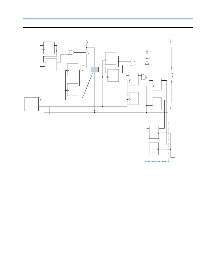
Altera Corporation
2–49
February 2005
Preliminary
I/O Structure
Figure 2–34. DDR SDRAM & FCRAM Interfacing
Programmable Drive Strength
The output buffer for each Cyclone device I/O pin has a programmable
drive strength control for certain I/O standards. The LVTTL and
LVCMOS standards have several levels of drive strength that the designer
can control. SSTL-3 class I and II, and SSTL-2 class I and II support a
minimum setting, the lowest drive strength that guarantees the I
OH
/I
OL
V
CC
GND
PLL
Phase Shifted -90
˚
DQS
Adjacent LAB LEs
Global Clock
Resynchronizing
Global Clock
Programmable
Delay Chain
Output LE
Register
Output LE
Registers
DQ
Input LE
Registers
Input LE
Registers
LE
Register
LE
Register
∆
t
Adjacent
LAB LEs
OE
OE LE
Register
OE LE
Register
OE
OE LE
Register
OE LE
Register
Output LE
Registers
Output LE
Register
DataA
DataB
clk
-90˚ clk
FPGA_cyc-html.html
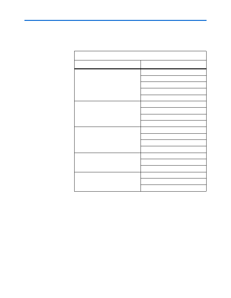
2–50
Altera
Corporation
Preliminary
February 2005
Cyclone Device Handbook, Volume 1
of the standard. Using minimum settings provides signal slew rate
control to reduce system noise and signal overshoot.
Table 2–11
shows the
possible settings for the I/O standards with drive strength control.
Open-Drain Output
Cyclone devices provide an optional open-drain (equivalent to an open-
collector) output for each I/O pin. This open-drain output enables the
device to provide system-level control signals (e.g., interrupt and write-
enable signals) that can be asserted by any of several devices.
Slew-Rate Control
The output buffer for each Cyclone device I/O pin has a programmable
output slew-rate control that can be configured for low noise or high-
speed performance. A faster slew rate provides high-speed transitions for
high-performance systems. However, these fast transitions may
introduce noise transients into the system. A slow slew rate reduces
Table 2–11. Programmable Drive Strength
I/O Standard
I
OH
/I
OL
Current Strength Setting (mA)
LVTTL (3.3 V)
4
8
12
16
24
LVCMOS (3.3 V)
2
4
8
12
LVTTL (2.5 V)
2
8
12
16
LVTTL (1.8 V)
2
8
12
LVCMOS (1.5 V)
2
4
8
FPGA_cyc-html.html

Altera Corporation
2–51
February 2005
Preliminary
I/O Structure
system noise, but adds a nominal delay to rising and falling edges. Each
I/O pin has an individual slew-rate control, allowing the designer to
specify the slew rate on a pin-by-pin basis. The slew-rate control affects
both the rising and falling edges.
Bus Hold
Each Cyclone device I/O pin provides an optional bus-hold feature. The
bus-hold circuitry can hold the signal on an I/O pin at its last-driven
state. Since the bus-hold feature holds the last-driven state of the pin until
the next input signal is present, an external pull-up or pull-down resistor
is not necessary to hold a signal level when the bus is tri-stated.
The bus-hold circuitry also pulls undriven pins away from the input
threshold voltage where noise can cause unintended high-frequency
switching. The designer can select this feature individually for each I/O
pin. The bus-hold output will drive no higher than V
CCIO
to prevent
overdriving signals. If the bus-hold feature is enabled, the device cannot
use the programmable pull-up option. Disable the bus-hold feature when
the I/O pin is configured for differential signals.
The bus-hold circuitry uses a resistor with a nominal resistance (RBH) of
approximately 7 k
Ω
to pull the signal level to the last-driven state.
Table 4–15 on page 4–6
gives the specific sustaining current for each
V
CCIO
voltage level driven through this resistor and overdrive current
used to identify the next-driven input level.
The bus-hold circuitry is only active after configuration. When going into
user mode, the bus-hold circuit captures the value on the pin present at
the end of configuration.
Programmable Pull-Up Resistor
Each Cyclone device I/O pin provides an optional programmable pull-
up resistor during user mode. If the designer enables this feature for an
I/O pin, the pull-up resistor (typically 25 k
Ω
) holds the output to the
V
CCIO
level of the output pin's bank. Dedicated clock pins do not have the
optional programmable pull-up resistor.
FPGA_cyc-html.html
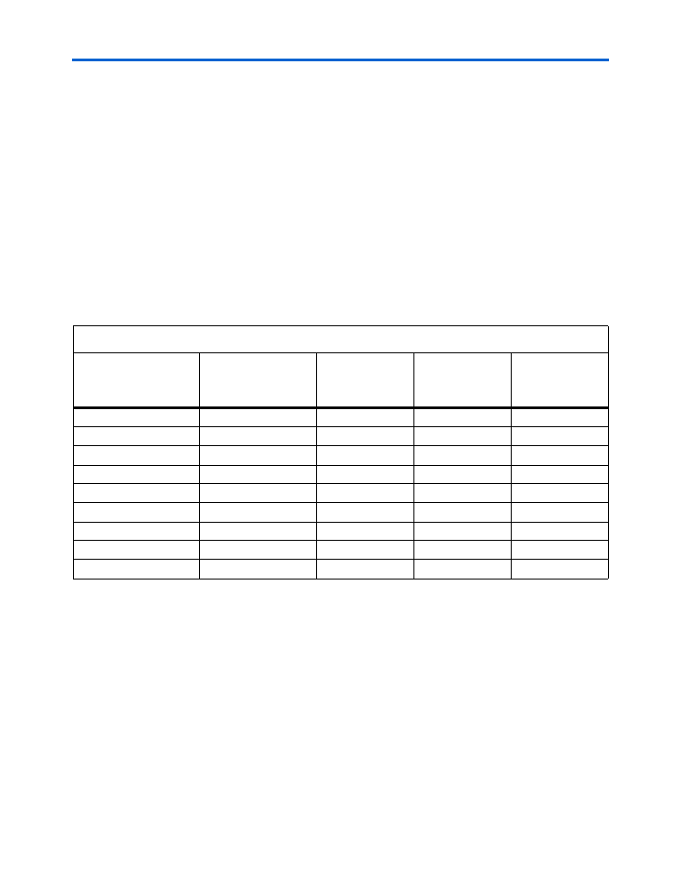
2–52
Altera
Corporation
Preliminary
February 2005
Cyclone Device Handbook, Volume 1
Advanced I/O Standard Support
Cyclone device IOEs support the following I/O standards:
■
3.3-V LVTTL/LVCMOS
■
2.5-V LVTTL/LVCMOS
■
1.8-V LVTTL/LVCMOS
■
1.5-V LVCMOS
■
3.3-V PCI
■
LVDS
■
SSTL-2 class I and II
■
SSTL-3 class I and II
■
Differential SSTL-2 class II (on output clocks only)
Table 2–12
describes the I/O standards supported by Cyclone devices.
Cyclone devices contain four I/O banks, as shown in
Figure 2–35
. I/O
banks 1 and 3 support all the I/O standards listed in
Table 2–12
. I/O
banks 2 and 4 support all the I/O standards listed in
Table 2–12
except the
3.3-V PCI standard. I/O banks 2 and 4 contain dual-purpose DQS, DQ,
and DM pins to support a DDR SDRAM or FCRAM interface. I/O bank
1 can also support a DDR SDRAM or FCRAM interface, however, the
Table 2–12. Cyclone I/O Standards
I/O Standard
Type
Input Reference
Voltage (V
REF
) (V)
Output Supply
Voltage (V
CCIO
) (V)
Board
Termination
Voltage (V
TT
) (V)
3.3-V LVTTL/LVCMOS
Single-ended
N/A
3.3
N/A
2.5-V LVTTL/LVCMOS
Single-ended
N/A
2.5
N/A
1.8-V LVTTL/LVCMOS
Single-ended
N/A
1.8
N/A
1.5-V LVCMOS
Single-ended
N/A
1.5
N/A
3.3-V PCI
(1)
Single-ended
N/A
3.3
N/A
LVDS
(2)
Differential
N/A
2.5
N/A
SSTL-2 class I and II
Voltage-referenced
1.25
2.5
1.25
SSTL-3 class I and II
Voltage-referenced
1.5
3.3
1.5
Differential SSTL-2
(3)
Differential
1.25
2.5
1.25
Notes to
Table 2–12
:
(1)
EP1C3 devices support PCI by using the LVTTL 16-mA I/O standard and drive strength assignments in the
Quartus II software. The device requires an external diode for PCI compliance.
(2)
EP1C3 devices in the 100-pin TQFP package do not support the LVDS I/O standard.
(3)
This I/O standard is only available on output clock pins (
PLL_OUT
pins).
FPGA_cyc-html.html
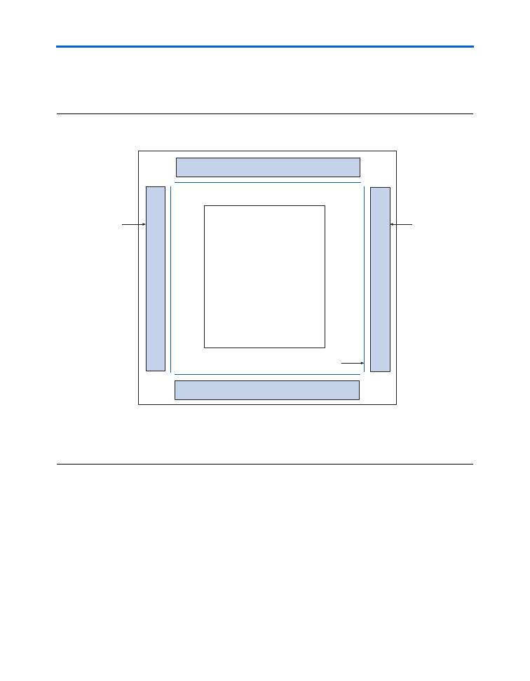
Altera Corporation
2–53
February 2005
Preliminary
I/O Structure
configuration input pins in I/O bank 1 must operate at 2.5 V. I/O bank 3
can also support a DDR SDRAM or FCRAM interface, however, all the
JTAG pins in I/O bank 3 must operate at 2.5 V.
Figure 2–35. Cyclone I/O Banks
Notes (1)
,
(2)
Notes to
Figure 2–35
:
(1)
Figure 2–35
is a top view of the silicon die.
(2)
Figure 2–35
is a graphic representation only. Refer to the pin list and the Quartus II software for exact pin locations.
Each I/O bank has its own
VCCIO
pins. A single device can support 1.5-V,
1.8-V, 2.5-V, and 3.3-V interfaces; each individual bank can support a
different standard with different I/O voltages. Each bank also has dual-
purpose
VREF
pins to support any one of the voltage-referenced
standards (e.g., SSTL-3) independently. If an I/O bank does not use
voltage-referenced standards, the V
REF
pins are available as user I/O pins.
Each I/O bank can support multiple standards with the same V
CCIO
for
input and output pins. For example, when V
CCIO
is 3.3-V, a bank can
support LVTTL, LVCMOS, 3.3-V PCI, and SSTL-3 for inputs and outputs.
I/O Bank 2
I/O Bank 3
I/O Bank 4
I/O Bank 1
All I/O Banks Support
■
3.3-V LVTTL/LVCMOS
■
2.5-V LVTTL/LVCMOS
■
1.8-V LVTTL/LVCMOS
■
1.5-V LVCMOS
■
LVDS
■
SSTL-2 Class I and II
■
SSTL-3 Class I and II
I/O Bank 3
Also Supports
the 3.3-V PCI
I/O Standard
I/O Bank 1
Also Supports
the 3.3-V PCI
I/O Standard
Individual
Power Bus
FPGA_cyc-html.html
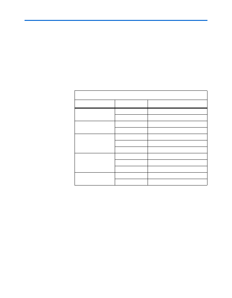
2–54
Altera
Corporation
Preliminary
February 2005
Cyclone Device Handbook, Volume 1
LVDS I/O Pins
A subset of pins in all four I/O banks supports LVDS interfacing. These
dual-purpose LVDS pins require an external-resistor network at the
transmitter channels in addition to 100-
Ω
termination resistors on
receiver channels. These pins do not contain dedicated serialization or
deserialization circuitry; therefore, internal logic performs serialization
and deserialization functions.
Table 2–13
shows the total number of supported LVDS channels per
device density.
MultiVolt I/O Interface
The Cyclone architecture supports the MultiVolt I/O interface feature,
which allows Cyclone devices in all packages to interface with systems of
different supply voltages. The devices have one set of V
CC
pins for
internal operation and input buffers (V
CCINT
), and four sets for I/O
output drivers (V
CCIO
).
The Cyclone V
CCINT
pins must always be connected to a 1.5-V power
supply. If the V
CCINT
level is 1.5 V, then input pins are 1.5-V, 1.8-V, 2.5-V,
and 3.3-V tolerant. The V
CCIO
pins can be connected to either a 1.5-V, 1.8-V,
Table 2–13. Cyclone Device LVDS Channels
Device
Pin Count
Number of LVDS Channels
EP1C3
100
(1)
144
34
EP1C4
324
103
400
129
EP1C6
144
29
240
72
256
72
EP1C12
240
66
256
72
324
103
EP1C20
324
95
400
129
Note to
Table 2–13
:
(1)
EP1C3 devices in the 100-pin TQFP package do not support the LVDS I/O
standard.
FPGA_cyc-html.html
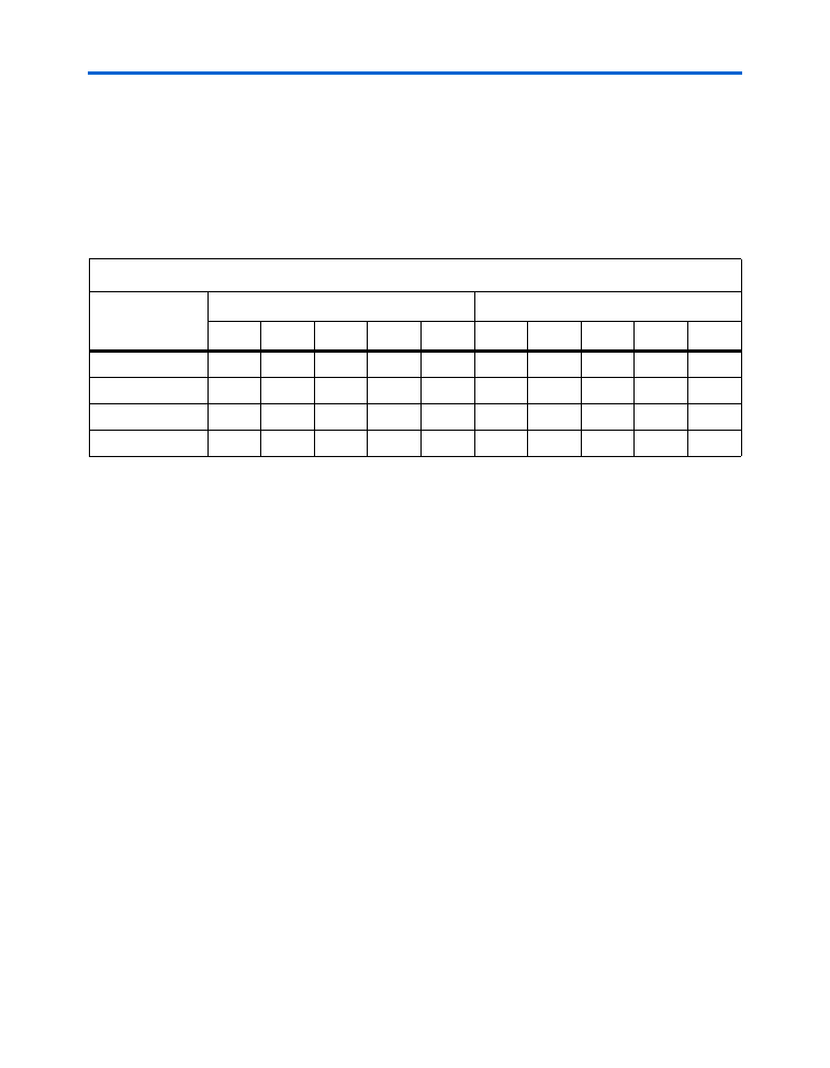
Altera Corporation
2–55
February 2005
Preliminary
Power Sequencing & Hot Socketing
2.5-V, or 3.3-V power supply, depending on the output requirements. The
output levels are compatible with systems of the same voltage as the
power supply (i.e., when V
CCIO
pins are connected to a 1.5-V power
supply, the output levels are compatible with 1.5-V systems). When V
CCIO
pins are connected to a 3.3-V power supply, the output high is 3.3-V and
is compatible with 3.3-V or 5.0-V systems.
Table 2–14
summarizes
Cyclone MultiVolt I/O support.
Power
Sequencing &
Hot Socketing
Because Cyclone devices can be used in a mixed-voltage environment,
they have been designed specifically to tolerate any possible power-up
sequence. Therefore, the V
CCIO
and V
CCINT
power supplies may be
powered in any order.
Signals can be driven into Cyclone devices before and during power up
without damaging the device. In addition, Cyclone devices do not drive
out during power up. Once operating conditions are reached and the
device is configured, Cyclone devices operate as specified by the user.
Table 2–14. Cyclone MultiVolt I/O Support
Note (1)
V
CCIO
(V)
Input Signal
Output Signal
1.5 V
1.8 V
2.5 V
3.3 V
5.0 V
1.5 V
1.8 V
2.5 V
3.3 V
5.0 V
1.5
v
v
v
(2)
v
(2)
v
1.8
v
v
v
v
(3)
v
2.5
v
v
v
(5)
v
(5)
v
3.3
v
(4)
v
v
(6)
v
(7)
v
(7)
v
(7)
v
v
(8)
Notes to
Table 2–14
:
(1)
The PCI clamping diode must be disabled to drive an input with voltages higher than V
CCIO
.
(2)
When V
CCIO
= 1.5-V and a 2.5-V or 3.3-V input signal feeds an input pin, higher pin leakage current is expected.
(3)
When V
CCIO
= 1.8-V, a Cyclone device can drive a 1.5-V device with 1.8-V tolerant inputs.
(4)
When V
CCIO
= 3.3-V and a 2.5-V input signal feeds an input pin, the V
CCIO
supply current will be slightly larger
than expected.
(5)
When V
CCIO
= 2.5-V, a Cyclone device can drive a 1.5-V or 1.8-V device with 2.5-V tolerant inputs.
(6)
Cyclone devices can be 5.0-V tolerant with the use of an external resistor and the internal PCI clamp diode.
(7)
When V
CCIO
= 3.3-V, a Cyclone device can drive a 1.5-V, 1.8-V, or 2.5-V device with 3.3-V tolerant inputs.
(8)
When V
CCIO
= 3.3-V, a Cyclone device can drive a device with 5.0-V LVTTL inputs but not 5.0-V LVCMOS inputs.
FPGA_cyc-html.html

2–56
Altera
Corporation
Preliminary
February 2005
Cyclone Device Handbook, Volume 1
FPGA_cyc-html.html
Altera Corporation
3–1
February 2005
Preliminary
3. Configuration & Testing
IEEE Std. 1149.1
(JTAG) Boundary
Scan Support
All Cyclone devices provide JTAG BST circuitry that complies with the
IEEE Std. 1149.1a-1990 specification. JTAG boundary-scan testing can be
performed either before or after, but not during configuration. Cyclone
devices can also use the JTAG port for configuration together with either
the Quartus
®
II software or hardware using either Jam Files (
.jam
) or Jam
Byte-Code Files (
.jbc
).
Cyclone devices support reconfiguring the I/O standard settings on the
IOE through the JTAG BST chain. The JTAG chain can update the I/O
standard for all input and output pins any time before or during user
mode. Designers can use this ability for JTAG testing before configuration
when some of the Cyclone pins drive or receive from other devices on the
board using voltage-referenced standards. Since the Cyclone device
might not be configured before JTAG testing, the I/O pins might not be
configured for appropriate electrical standards for chip-to-chip
communication. Programming those I/O standards via JTAG allows
designers to fully test I/O connection to other devices.
The JTAG pins support 1.5-V/1.8-V or 2.5-V/3.3-V I/O standards. The
TDO pin voltage is determined by the V
CCIO
of the bank where it resides.
The bank V
CCIO
selects whether the JTAG inputs are 1.5-V, 1.8-V, 2.5-V, or
3.3-V compatible.
Cyclone devices also use the JTAG port to monitor the operation of the
device with the SignalTap
®
II embedded logic analyzer. Cyclone devices
support the JTAG instructions shown in
Table 3–1
.
Table 3–1. Cyclone JTAG Instructions (Part 1 of 2)
JTAG Instruction
Instruction Code
Description
SAMPLE
/
PRELOAD
00 0000 0101
Allows a snapshot of signals at the device pins to be captured and
examined during normal device operation, and permits an initial
data pattern to be output at the device pins. Also used by the
SignalTap II embedded logic analyzer.
EXTEST
(1)
00 0000 0000
Allows the external circuitry and board-level interconnects to be
tested by forcing a test pattern at the output pins and capturing test
results at the input pins.
BYPASS
11 1111 1111
Places the 1-bit bypass register between the
TDI
and
TDO
pins,
which allows the BST data to pass synchronously through selected
devices to adjacent devices during normal device operation.
C51003-1.1
FPGA_cyc-html.html

3–2
Altera
Corporation
Preliminary
February 2005
Cyclone Device Handbook, Volume 1
USERCODE
00 0000 0111
Selects the 32-bit USERCODE register and places it between the
TDI
and
TDO
pins, allowing the USERCODE to be serially shifted
out of
TDO
.
IDCODE
00 0000 0110
Selects the IDCODE register and places it between
TDI
and
TDO
,
allowing the IDCODE to be serially shifted out of
TDO
.
HIGHZ
(1)
00 0000 1011
Places the 1-bit bypass register between the
TDI
and
TDO
pins,
which allows the BST data to pass synchronously through selected
devices to adjacent devices during normal device operation, while
tri-stating all of the I/O pins.
CLAMP
(1)
00 0000 1010
Places the 1-bit bypass register between the
TDI
and
TDO
pins,
which allows the BST data to pass synchronously through selected
devices to adjacent devices during normal device operation while
holding I/O pins to a state defined by the data in the boundary-scan
register.
ICR instructions
Used when configuring a Cyclone device via the JTAG port with a
MasterBlaster
TM
or ByteBlasterMV
TM
download cable, or when
using a Jam File or Jam Byte-Code File via an embedded
processor.
PULSE_NCONFIG
00 0000 0001
Emulates pulsing the
nCONFIG
pin low to trigger reconfiguration
even though the physical pin is unaffected.
CONFIG_IO
00 0000 1101
Allows configuration of I/O standards through the JTAG chain for
JTAG testing. Can be executed before, after, or during
configuration. Stops configuration if executed during configuration.
Once issued, the
CONFIG_IO
instruction will hold
nSTATUS
low
to reset the configuration device.
nSTATUS
is held low until the
device is reconfigured.
SignalTap II
instructions
Monitors internal device operation with the SignalTap II embedded
logic analyzer.
Note to
Table 3–1
:
(1)
Bus hold and weak pull-up resistor features override the high-impedance state of
HIGHZ
,
CLAMP
, and
EXTEST
.
Table 3–1. Cyclone JTAG Instructions (Part 2 of 2)
JTAG Instruction
Instruction Code
Description
FPGA_cyc-html.html
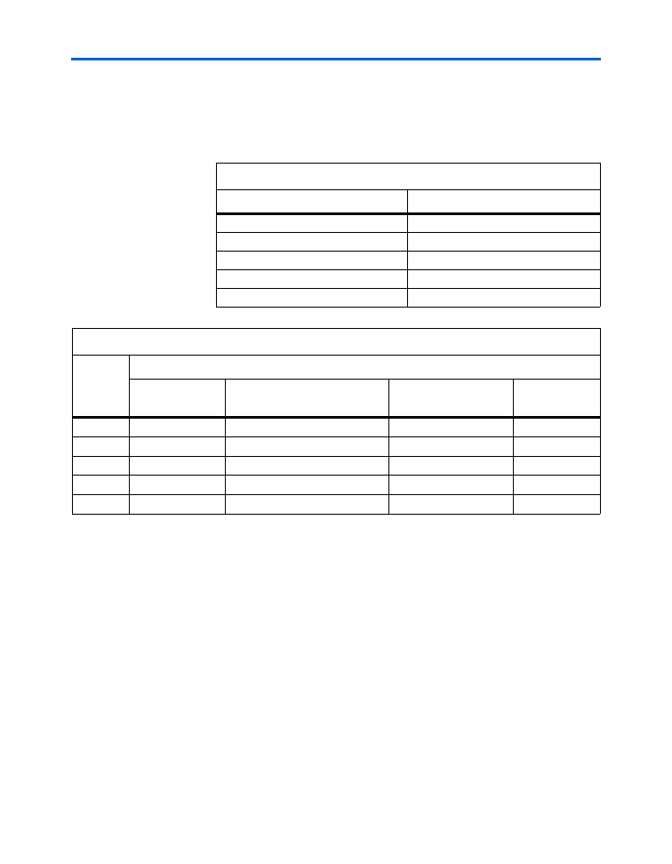
Altera Corporation
3–3
February 2005
Preliminary
IEEE Std. 1149.1 (JTAG) Boundary Scan Support
The Cyclone device instruction register length is 10 bits and the
USERCODE register length is 32 bits.
Tables 3–2
and
3–3
show the
boundary-scan register length and device IDCODE information for
Cyclone devices.
Table 3–2. Cyclone Boundary-Scan Register Length
Device
Boundary-Scan Register Length
EP1C3
339
EP1C4
930
EP1C6
582
EP1C12
774
EP1C20
930
Table 3–3. 32-Bit Cyclone Device IDCODE
Device
IDCODE (32 bits)
(1)
Version (4 Bits)
Part Number (16 Bits)
Manufacturer Identity
(11 Bits)
LSB (1 Bit)
(2)
EP1C3
0000
0010 0000 1000 0001
000 0110 1110
1
EP1C4
0000
0010 0000 1000 0101
000 0110 1110
1
EP1C6
0000
0010 0000 1000 0010
000 0110 1110
1
EP1C12
0000
0010 0000 1000 0011
000 0110 1110
1
EP1C20
0000
0010 0000 1000 0100
000 0110 1110
1
Notes to
Table 3–3
:
(1)
The most significant bit (MSB) is on the left.
(2)
The IDCODE’s least significant bit (LSB) is always
1
.
FPGA_cyc-html.html
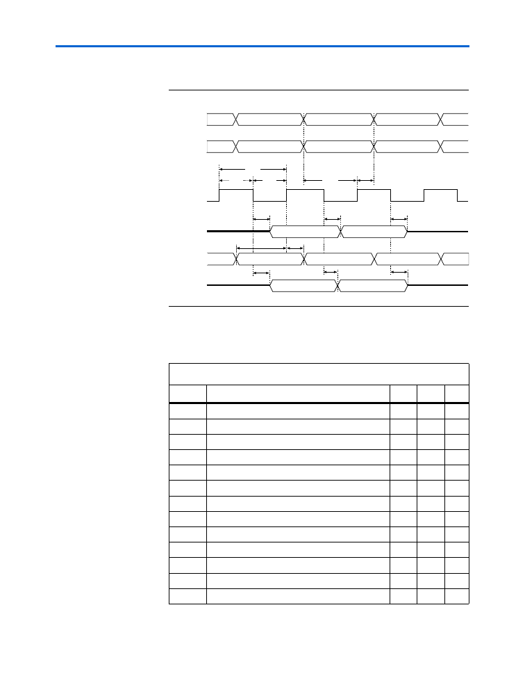
3–4
Altera
Corporation
Preliminary
February 2005
Cyclone Device Handbook, Volume 1
Figure 3–1
shows the timing requirements for the JTAG signals.
Figure 3–1. Cyclone JTAG Waveforms
Table 3–4
shows the JTAG timing parameters and values for Cyclone
devices.
Table 3–4. Cyclone JTAG Timing Parameters & Values
Symbol
Parameter
Min
Max
Unit
t
J C P
TCK
clock period
100
ns
t
J C H
TCK
clock high time
50
ns
t
J C L
TCK
clock low time
50
ns
t
J P S U
JTAG port setup time
20
ns
t
J P H
JTAG port hold time
45
ns
t
J P C O
JTAG port clock to output
25
ns
t
J P Z X
JTAG port high impedance to valid output
25
ns
t
J P X Z
JTAG port valid output to high impedance
25
ns
t
J S S U
Capture register setup time
20
ns
t
J S H
Capture register hold time
45
ns
t
J S C O
Update register clock to output
35
ns
t
J S Z X
Update register high impedance to valid output
35
ns
t
J S X Z
Update register valid output to high impedance
35
ns
TDO
TCK
t
JPZX
t
JPCO
t
JPH
t
JPXZ
t
JCP
t
JPSU
t
JCL
t
JCH
TDI
TMS
Signal
to Be
Captured
Signal
to Be
Driven
t
JSZX
t
JSSU
t
JSH
t
JSCO
t
JSXZ
FPGA_cyc-html.html

Altera Corporation
3–5
February 2005
Preliminary
SignalTap II Embedded Logic Analyzer
1
Cyclone devices must be within the first 17 devices in a JTAG
chain. All of these devices have the same JTAG controller. If any
of the Cyclone devices are in the 18th or after they will fail
configuration. This does not affect the SignalTap
®
II logic
analyzer.
f
For more information on JTAG, see the following documents:
■
AN 39: IEEE Std. 1149.1 (JTAG) Boundary-Scan Testing in Altera
Devices
■
Jam Programming & Test Language Specification
SignalTap II
Embedded Logic
Analyzer
Cyclone devices feature the SignalTap II embedded logic analyzer, which
monitors design operation over a period of time through the IEEE
Std. 1149.1 (JTAG) circuitry. A designer can analyze internal logic at
speed without bringing internal signals to the I/O pins. This feature is
particularly important for advanced packages, such as FineLine BGA
packages, because it can be difficult to add a connection to a pin during
the debugging process after a board is designed and manufactured.
Configuration
The logic, circuitry, and interconnects in the Cyclone architecture are
configured with CMOS SRAM elements. Altera FPGAs are
reconfigurable and every device is tested with a high coverage
production test program so the designer does not have to perform fault
testing and can instead focus on simulation and design verification.
Cyclone devices are configured at system power-up with data stored in
an Altera configuration device or provided by a system controller. The
Cyclone device's optimized interface allows the device to act as controller
in an active serial configuration scheme with the new low-cost serial
configuration device. Cyclone devices can be configured in under 120 ms
using serial data at 20 MHz. The serial configuration device can be
programmed via the ByteBlaster II download cable, the Altera
Programming Unit (APU), or third-party programmers.
In addition to the new low-cost serial configuration device, Altera offers
in-system programmability (ISP)-capable configuration devices that can
configure Cyclone devices via a serial data stream. The interface also
enables microprocessors to treat Cyclone devices as memory and
configure them by writing to a virtual memory location, making
reconfiguration easy. After a Cyclone device has been configured, it can
be reconfigured in-circuit by resetting the device and loading new data.
Real-time changes can be made during system operation, enabling
innovative reconfigurable computing applications.
FPGA_cyc-html.html

3–6
Altera
Corporation
Preliminary
February 2005
Cyclone Device Handbook, Volume 1
Operating Modes
The Cyclone architecture uses SRAM configuration elements that require
configuration data to be loaded each time the circuit powers up. The
process of physically loading the SRAM data into the device is called
configuration. During initialization, which occurs immediately after
configuration, the device resets registers, enables I/O pins, and begins to
operate as a logic device. Together, the configuration and initialization
processes are called command mode. Normal device operation is called
user mode.
SRAM configuration elements allow Cyclone devices to be reconfigured
in-circuit by loading new configuration data into the device. With real-
time reconfiguration, the device is forced into command mode with a
device pin. The configuration process loads different configuration data,
reinitializes the device, and resumes user-mode operation. Designers can
perform in-field upgrades by distributing new configuration files either
within the system or remotely.
A built-in weak pull-up resistor pulls all user I/O pins to V
CCIO
before
and during device configuration.
The configuration pins support 1.5-V/1.8-V or 2.5-V/3.3-V I/O
standards. The voltage level of the configuration output pins is
determined by the V
CCIO
of the bank where the pins reside. The bank
V
CCIO
selects whether the configuration inputs are 1.5-V, 1.8-V, 2.5-V, or
3.3-V compatible.
Configuration Schemes
Designers can load the configuration data for a Cyclone device with one
of three configuration schemes (see
Table 3–5
), chosen on the basis of the
target application. Designers can use a configuration device, intelligent
controller, or the JTAG port to configure a Cyclone device. A low-cost
configuration device can automatically configure a Cyclone device at
system power-up.
FPGA_cyc-html.html
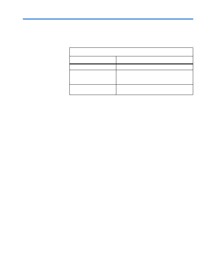
Altera Corporation
3–7
February 2005
Preliminary
Configuration
Multiple Cyclone devices can be configured in any of the three
configuration schemes by connecting the configuration enable (
nCE
) and
configuration enable output (
nCEO
) pins on each device.
Table 3–5. Data Sources for Configuration
Configuration Scheme
Data Source
Active serial
Low-cost serial configuration device
Passive serial (PS)
Enhanced or EPC2 configuration device,
MasterBlaster or ByteBlasterMV download cable,
or serial data source
JTAG
MasterBlaster or ByteBlasterMV download cable
or a microprocessor with a Jam or JBC file
FPGA_cyc-html.html

3–8
Altera
Corporation
Preliminary
February 2005
Cyclone Device Handbook, Volume 1
FPGA_cyc-html.html
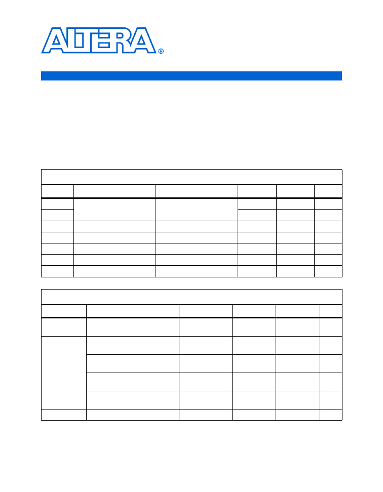
Altera Corporation
4–1
February 2005
Preliminary
4. DC & Switching
Characteristics
Operating
Conditions
Cyclone devices are offered in both commercial, industrial, and extended
temperature grades. However, industrial-grade and extended-
temperature-grade devices may have limited speed-grade availability.
Tables 4–1
through
4–16
provide information on absolute maximum
ratings, recommended operating conditions, DC operating conditions,
and capacitance for Cyclone devices.
Table 4–1. Cyclone Device Absolute Maximum Ratings
Notes (1)
,
(2)
Symbol
Parameter
Conditions
Minimum
Maximum
Unit
V
CCINT
Supply voltage
With respect to ground
(3)
–0.5
2.4
V
V
CCIO
–0.5
4.6
V
V
I
DC input voltage
–0.5
4.6
V
I
OUT
DC output current, per pin
–25
25
mA
T
STG
Storage temperature
No bias
–65
150
°
C
T
AMB
Ambient temperature
Under bias
–65
135
°
C
T
J
Junction temperature
BGA packages under bias
135
°
C
Table 4–2. Cyclone Device Recommended Operating Conditions (Part 1 of 2)
Symbol
Parameter
Conditions
Minimum
Maximum
Unit
V
CCINT
Supply voltage for internal logic
and input buffers
(4)
1.425
1.575
V
V
CCIO
Supply voltage for output buffers,
3.3-V operation
(4)
3.00
3.60
V
Supply voltage for output buffers,
2.5-V operation
(4)
2.375
2.625
V
Supply voltage for output buffers,
1.8-V operation
(4)
1.71
1.89
V
Supply voltage for output buffers,
1.5-V operation
(4)
1.4
1.6
V
V
I
Input voltage
(3)
,
(5)
–0.5
4.1
V
C51004-1.4
FPGA_cyc-html.html
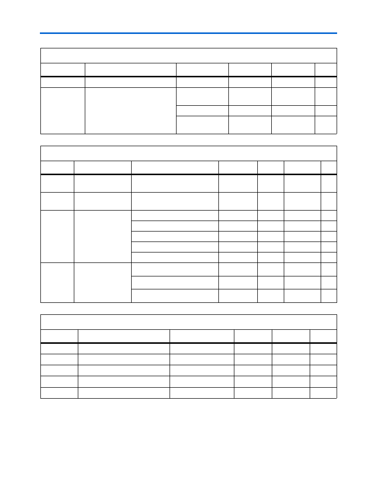
4–2
Altera
Corporation
Preliminary
February 2005
Cyclone Device Handbook, Volume 1
V
O
Output voltage
0
V
CCIO
V
T
J
Operating junction temperature
For commercial
use
0
85
°
C
For industrial use
–40
100
°
C
For extended-
temperature use
–40
125
°
C
Table 4–3. Cyclone Device DC Operating Conditions
Note (6)
Symbol
Parameter
Conditions
Minimum
Typical
Maximum
Unit
I
I
Input pin leakage
current
V
I
= V
C C I O m a x
to 0 V
(8)
–10
10
µ
A
I
OZ
Tri-stated I/O pin
leakage current
V
O
= V
C C I O m a x
to 0 V
(8)
–10
10
µ
A
I
CC0
V
CC
supply current
(standby) (All M4K
blocks in power-
down mode)
(7)
EP1C3
4
mA
EP1C4
6
mA
EP1C6
6
mA
EP1C12
8
mA
EP1C20
12
mA
R
CONF
Value of I/O pin pull-
up resistor before
and during
configuration
V
CCIO
= 3.6 V at –40
°
C
(9)
17
k
Ω
V
CCIO
= 3.3 V at 25
°
C
(9)
25
k
Ω
V
CCIO
= 3.0 V at 125
°
C
(9)
40
k
Ω
Table 4–4. LVTTL Specifications
Symbol
Parameter
Conditions
Minimum
Maximum
Unit
V
CCIO
Output supply voltage
3.0
3.6
V
V
I H
High-level input voltage
1.7
4.1
V
V
IL
Low-level input voltage
–0.5
0.7
V
V
OH
High-level output voltage
I
OH
= –4 to –24 mA
(10)
2.4
V
V
OL
Low-level output voltage
I
OL
= 4 to 24 mA
(10)
0.45
V
Table 4–2. Cyclone Device Recommended Operating Conditions (Part 2 of 2)
Symbol
Parameter
Conditions
Minimum
Maximum
Unit
FPGA_cyc-html.html
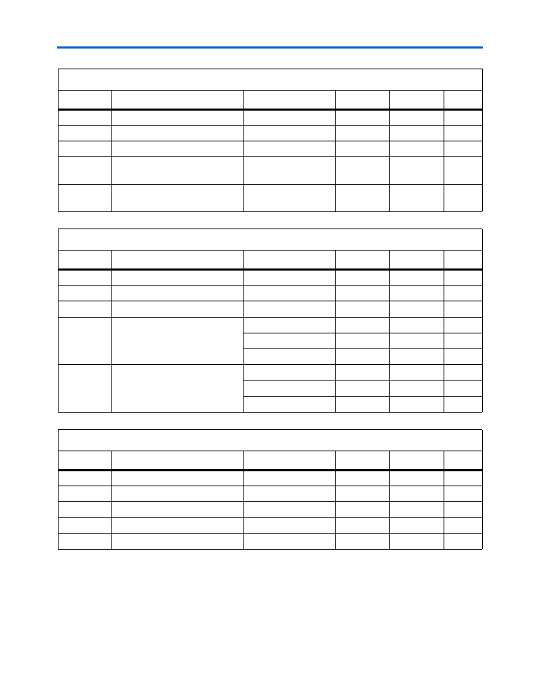
Altera Corporation
4–3
February 2005
Preliminary
Operating Conditions
Table 4–5. LVCMOS Specifications
Symbol
Parameter
Conditions
Minimum
Maximum
Unit
V
CCIO
Output supply voltage
3.0
3.6
V
V
IH
High-level input voltage
1.7
4.1
V
V
IL
Low-level input voltage
–0.5
0.7
V
V
OH
High-level output voltage
V
CCIO
= 3.0,
I
OH
= –0.1 mA
V
CCIO
– 0.2
V
V
OL
Low-level output voltage
V
CCIO
= 3.0,
I
OL
= 0.1 mA
0.2
V
Table 4–6. 2.5-V I/O Specifications
Symbol
Parameter
Conditions
Minimum
Maximum
Unit
V
CCIO
Output supply voltage
2.375
2.625
V
V
IH
High-level input voltage
1.7
4.1
V
V
IL
Low-level input voltage
–0.5
0.7
V
V
OH
High-level output voltage
I
OH
= –0.1 mA
2.1
V
I
OH
= –1 mA
2.0
V
I
OH
= –2 to –16 mA
(10)
1.7
V
V
OL
Low-level output voltage
I
OL
= 0.1 mA
0.2
V
I
OH
= 1 mA
0.4
V
I
OH
= 2 to 16 mA
(10)
0.7
V
Table 4–7. 1.8-V I/O Specifications
Symbol
Parameter
Conditions
Minimum
Maximum
Unit
V
CCIO
Output supply voltage
1.65
1.95
V
V
I H
High-level input voltage
0.65
×
V
CCIO
2.25
V
V
IL
Low-level input voltage
–0.3
0.35
×
V
CCIO
V
V
OH
High-level output voltage
I
OH
= –2 to –8 mA
(10)
V
CCIO
– 0.45
V
V
OL
Low-level output voltage
I
OL
= 2 to 8 mA
(10)
0.45
V
FPGA_cyc-html.html
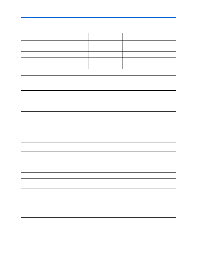
4–4
Altera
Corporation
Preliminary
February 2005
Cyclone Device Handbook, Volume 1
Table 4–8. 1.5-V I/O Specifications
Symbol
Parameter
Conditions
Minimum
Maximum
Unit
V
CCIO
Output supply voltage
1.4
1.6
V
V
I H
High-level input voltage
0.65
×
V
CCIO
V
CCIO
+ 0.3
V
V
IL
Low-level input voltage
–0.3
0.35
×
V
CCIO
V
V
OH
High-level output voltage
I
OH
= –2 mA
(10)
0.75
×
V
CCIO
V
V
OL
Low-level output voltage
I
OL
= 2 mA
(10)
0.25
×
V
CCIO
V
Table 4–9. 2.5-V LVDS I/O Specifications
Note (11)
Symbol
Parameter
Conditions
Minimum
Typical
Maximum
Unit
V
CCIO
I/O supply voltage
2.375
2.5
2.625
V
V
OD
Differential output voltage
R
L
= 100
Ω
250
550
mV
∆
V
OD
Change in V
OD
between
high and low
R
L
= 100
Ω
50
mV
V
OS
Output offset voltage
R
L
= 100
Ω
1.125
1.25
1.375
V
∆
V
OS
Change in V
OS
between
high and low
R
L
= 100
Ω
50
mV
V
TH
Differential input threshold
V
CM
= 1.2 V
–100
100
mV
V
IN
Receiver input voltage
range
0.0
2.4
V
R
L
Receiver differential input
resistor
90
100
110
Ω
Table 4–10. 3.3-V PCI Specifications
Symbol
Parameter
Conditions
Minimum
Typical
Maximum
Unit
V
CCIO
Output supply voltage
3.0
3.3
3.6
V
V
IH
High-level input voltage
0.5
×
V
CCIO
V
CCIO
+
0.5
V
V
IL
Low-level input voltage
–0.5
0.3
×
V
CCIO
V
V
OH
High-level output voltage
I
OUT
= –500
µ
A
0.9
×
V
CCIO
V
V
OL
Low-level output voltage
I
OUT
= 1,500
µ
A
0.1
×
V
CCIO
V
FPGA_cyc-html.html
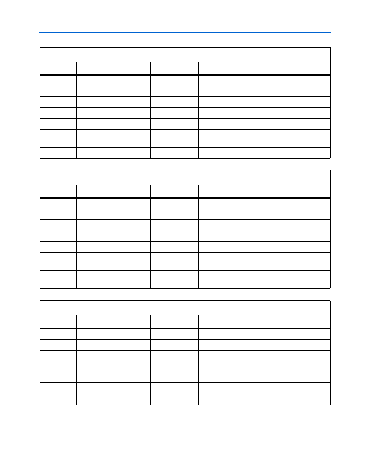
Altera Corporation
4–5
February 2005
Preliminary
Operating Conditions
Table 4–11. SSTL-2 Class I Specifications
Symbol
Parameter
Conditions
Minimum
Typical
Maximum
Unit
V
CCIO
Output supply voltage
2.375
2.5
2.625
V
V
TT
Termination voltage
V
R E F
– 0.04
V
R E F
V
R E F
+ 0.04
V
V
REF
Reference voltage
1.15
1.25
1.35
V
V
IH
High-level input voltage
V
R E F
+ 0.18
3.0
V
V
IL
Low-level input voltage
–0.3
V
R E F
– 0.18
V
V
OH
High-level output voltage
I
OH
= –8.1 mA
(10)
V
TT
+ 0.57
V
V
OL
Low-level output voltage
I
OL
= 8.1 mA
(10)
V
T T
– 0.57
V
Table 4–12. SSTL-2 Class II Specifications
Symbol
Parameter
Conditions
Minimum
Typical
Maximum
Unit
V
CCIO
Output supply voltage
2.3
2.5
2.7
V
V
TT
Termination voltage
V
R E F
– 0.04
V
R E F
V
R E F
+ 0.04
V
V
REF
Reference voltage
1.15
1.25
1.35
V
V
IH
High-level input voltage
V
R E F
+ 0.18
V
CCIO
+ 0.3
V
V
IL
Low-level input voltage
–0.3
V
R E F
– 0.18
V
V
OH
High-level output voltage
I
OH
= –16.4 mA
(10)
V
TT
+ 0.76
V
V
OL
Low-level output voltage
I
OL
= 16.4 mA
(10)
V
T T
– 0.76
V
Table 4–13. SSTL-3 Class I Specifications
Symbol
Parameter
Conditions
Minimum
Typical
Maximum
Unit
V
CCIO
Output supply voltage
3.0
3.3
3.6
V
V
TT
Termination voltage
V
R E F
– 0.05
V
R E F
V
R E F
+ 0.05
V
V
REF
Reference voltage
1.3
1.5
1.7
V
V
IH
High-level input voltage
V
R E F
+ 0.2
V
CCIO
+ 0.3
V
V
IL
Low-level input voltage
–0.3
V
R E F
– 0.2
V
V
OH
High-level output voltage
I
OH
= –8 mA
(10)
V
TT
+ 0.6
V
V
OL
Low-level output voltage
I
OL
= 8 mA
(10)
V
T T
– 0.6
V
FPGA_cyc-html.html
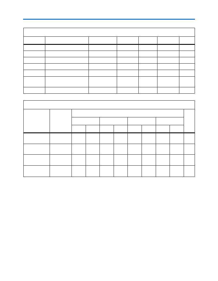
4–6
Altera
Corporation
Preliminary
February 2005
Cyclone Device Handbook, Volume 1
Table 4–14. SSTL-3 Class II Specifications
Symbol
Parameter
Conditions
Minimum
Typical
Maximum
Unit
V
CCIO
Output supply voltage
3.0
3.3
3.6
V
V
TT
Termination voltage
V
R E F
– 0.05
V
R E F
V
R E F
+ 0.05
V
V
REF
Reference voltage
1.3
1.5
1.7
V
V
IH
High-level input voltage
V
R E F
+ 0.2
V
CCIO
+ 0.3
V
V
IL
Low-level input voltage
–0.3
V
R E F
– 0.2
V
V
OH
High-level output voltage
I
OH
= –16 mA
(10)
V
T T
+ 0.8
V
V
OL
Low-level output voltage
I
OL
= 16 mA
(10)
V
TT
– 0.8
V
Table 4–15. Bus Hold Parameters
Parameter
Conditions
V
C C I O
Level
Unit
1.5 V
1.8 V
2.5 V
3.3 V
Min
Max
Min
Max
Min
Max
Min
Max
Low sustaining
current
V
IN
> V
IL
(maximum)
30
50
70
µ
A
High sustaining
current
V
IN
< V
IH
(minimum)
–30
–50
–70
µ
A
Low overdrive
current
0 V < V
IN
<
V
CCIO
200
300
500
µ
A
High overdrive
current
0 V < V
IN
<
V
CCIO
–200
–300
–500
µ
A
FPGA_cyc-html.html
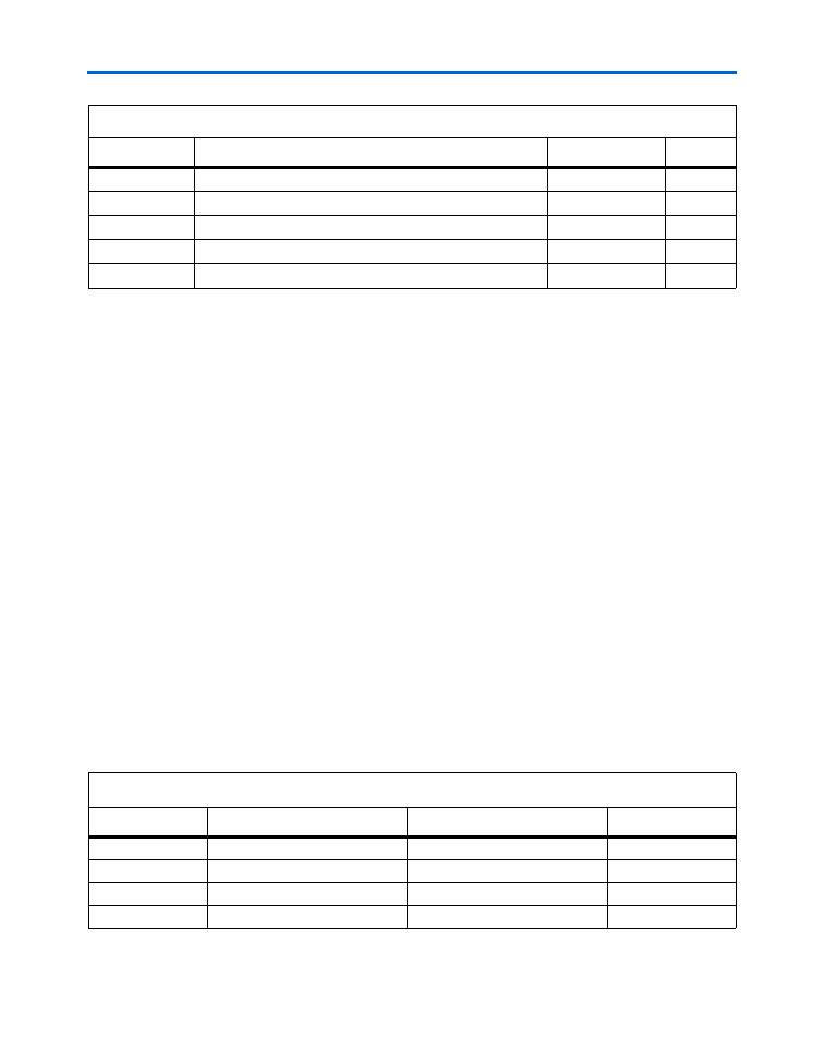
Altera Corporation
4–7
February 2005
Preliminary
Power Consumption
Power
Consumption
Designers can use the Altera web power calculator to estimate the device
power.
Cyclone devices require a certain amount of power-up current to
successfully power up because of the nature of the leading-edge process
on which they are fabricated.
Table 4–17
shows the maximum power-up
current required to power up a Cyclone device.
Table 4–16. Cyclone Device Capacitance
Note (12)
Symbol
Parameter
Typical
Unit
C
IO
Input capacitance for user I/O pin
4.0
pF
C
LVDS
Input capacitance for dual-purpose LVDS/user I/O pin
4.7
pF
C
VREF
Input capacitance for dual-purpose V
R E F
/user I/O pin.
12.0
pF
C
DPCLK
Input capacitance for dual-purpose
DPCLK
/user I/O pin.
4.4
pF
C
CLK
Input capacitance for CLK pin.
4.7
pF
Notes to
Tables 4–1
through
4–16
:
(1)
See the
Operating Requirements for Altera Devices Data Sheet
.
(2)
Conditions beyond those listed in
Table 4–1
may cause permanent damage to a device. Additionally, device
operation at the absolute maximum ratings for extended periods of time may have adverse affects on the device.
(3)
Minimum DC input is –0.5 V. During transitions, the inputs may undershoot to –2.0 V or overshoot to 4.6 V for
input currents less than 100 mA and periods shorter than 20 ns.
(4)
Maximum V
CC
rise time is 100 ms, and V
CC
must rise monotonically.
(5)
All pins, including dedicated inputs, clock, I/O, and JTAG pins, may be driven before V
CCINT
and V
CCIO
are
powered.
(6)
Typical values are for T
A
= 25
°
C, V
CCINT
= 1.5 V, and V
CCIO
= 1.5 V, 1.8 V, 2.5 V, and 3.3 V.
(7)
V
I
= ground, no load, no toggling inputs.
(8)
This value is specified for normal device operation. The value may vary during power-up. This applies for all
V
CCIO
settings (3.3, 2.5, 1.8, and 1.5 V).
(9)
Pin pull-up resistance values will lower if an external source drives the pin higher than V
CCIO
.
(10) Drive strength is programmable according to values in
Table 4–14
.
(11) The Cyclone LVDS interface requires a resistor network outside of the transmitter channels.
(12) Capacitance is sample-tested only. Capacitance is measured using time-domain reflections (TDR). Measurement
accuracy is within
±
0.5 pF.
Table 4–17. Cyclone Maximum Power-Up Current (I
CCINT
) Requirements (In-Rush Current) (Part 1 of 2)
Device
Commercial Specification
Industrial Specification
Unit
EP1C3
150
180
mA
EP1C4 150
180
mA
EP1C6 175
210
mA
EP1C12
300
360
mA
FPGA_cyc-html.html

4–8
Altera
Corporation
Preliminary
February 2005
Cyclone Device Handbook, Volume 1
Designers should select power supplies and regulators that can supply
this amount of current when designing with Cyclone devices. This
specification is for commercial operating conditions. Measurements were
performed with an isolated Cyclone device on the board. Decoupling
capacitors were not used in this measurement. To factor in the current for
decoupling capacitors, sum up the current for each capacitor using the
following equation:
I = C (dV/dt)
The exact amount of current that is consumed varies according to the
process, temperature, and power ramp rate. If the power supply or
regulator can supply more current than required, the Cyclone device may
consume more current than the maximum current specified in
Table 4–17
.
However, the device does not require any more current to successfully
power up than what is listed in
Table 4–17
.
The duration of the I
CCINT
power-up requirement depends on the V
CCINT
voltage supply rise time. The power-up current consumption drops when
the V
CCINT
supply reaches approximately 0.75 V. For example, if the
V
CCINT
rise time has a linear rise of 15 ms, the current consumption spike
drops by 7.5 ms.
Typically, the user-mode current during device operation is lower than
the power-up current in
Table 4–17
. Altera recommends using the
Cyclone Power Calculator, available on the Altera web site, to estimate
the user-mode I
CCINT
consumption and then select power supplies or
regulators based on the higher value.
Timing Model
The DirectDrive technology and MultiTrack interconnect ensure
predictable performance, accurate simulation, and accurate timing
analysis across all Cyclone device densities and speed grades. This
section describes and specifies the performance, internal, external, and
PLL timing specifications.
EP1C20
500
600
mA
Notes to
Table 4–17
:
(1)
The Cyclone devices (except for the EP1C20 device) meet the power up specification for Mini PCI.
(2)
The lot codes 9G0082 to 9G2999, or 9G3109 and later comply to the specifications in
Table 4–17
and meet the Mini
PCI specification. Lot codes appear at the top of the device.
(3)
The lot codes 9H0004 to 9H29999, or 9H3014 and later comply to the specifications in this table and meet the Mini
PCI specification. Lot codes appear at the top of the device.
Table 4–17. Cyclone Maximum Power-Up Current (I
CCINT
) Requirements (In-Rush Current) (Part 2 of 2)
Device
Commercial Specification
Industrial Specification
Unit
FPGA_cyc-html.html
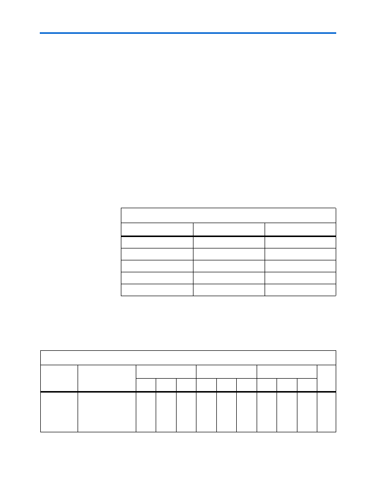
Altera Corporation
4–9
February 2005
Preliminary
Timing Model
All specifications are representative of worst-case supply voltage and
junction temperature conditions.
Preliminary & Final Timing
Timing models can have either preliminary or final status. The
Quartus
®
II software issues an informational message during the design
compilation if the timing models are preliminary.
Table 4–18
shows the
status of the Cyclone device timing models.
Preliminary status means the timing model is subject to change. Initially,
timing numbers are created using simulation results, process data, and
other known parameters. These tests are used to make the preliminary
numbers as close to the actual timing parameters as possible.
Final timing numbers are based on actual device operation and testing.
These numbers reflect the actual performance of the device under
worst-case voltage and junction temperature conditions.
Performance
The maximum internal logic array clock tree frequency is limited to the
specifications shown in
Table 4–19
.
Table 4–18. Cyclone Device Timing Model Status
Device
Preliminary
Final
EP1C3
v
EP1C4
v
EP1C6
v
EP1C12
v
EP1C20
v
Table 4–19. Clock Tree Maximum Performance Specification
Parameter
Definition
-6 Speed Grade
-7 Speed Grade
-8 Speed Grade
Units
Min
Typ
Max
Min
Typ
Max
Min
Typ
Max
Clock tree
f
M A X
Maximum frequency
that the clock tree
can support for
clocking registered
logic
405
320
275
MHz
FPGA_cyc-html.html
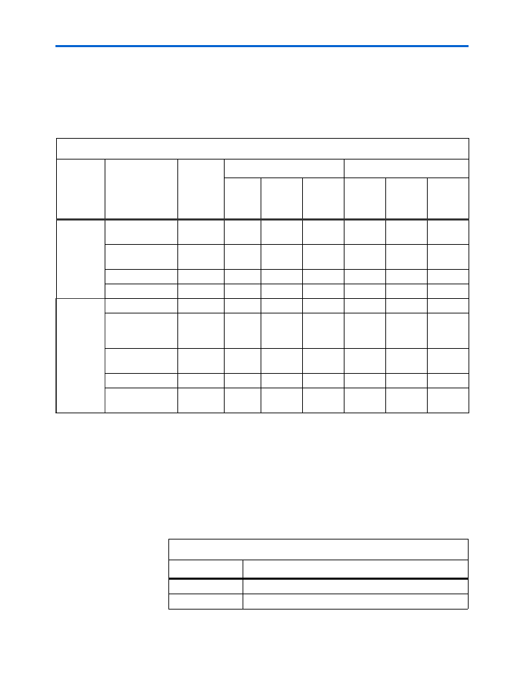
4–10
Altera
Corporation
Preliminary
February 2005
Cyclone Device Handbook, Volume 1
Table 4–20
shows the Cyclone device performance for some common
designs. All performance values were obtained with the Quartus II
software compilation of library of parameterized modules (LPM)
functions or megafunctions. These performance values are based on
EP1C6 devices in 144-pin TQFP packages.
Internal Timing Parameters
Internal timing parameters are specified on a speed grade basis
independent of device density.
Tables 4–21
through
4–24
describe the
Cyclone device internal timing microparameters for LEs, IOEs, M4K
memory structures, and MultiTrack interconnects.
Table 4–20. Cyclone Device Performance
Resource
Used
Design Size &
Function
Mode
Resources Used
Performance
LEs
M4K
Memory
Bits
M4K
Memory
Blocks
-6 Speed
Grade
(MHz)
-7 Speed
Grade
(MHz)
-8 Speed
Grade
(MHz)
LE
16-to-1
multiplexer
-
21
-
-
405.00
320.00
275.00
32-to-1
multiplexer
-
44
-
-
317.36
284.98
260.15
16-bit counter
-
16
-
-
405.00
320.00
275.00
64-bit counter
(1)
-
66
-
-
208.99
181.98
160.75
M4K
memory
block
RAM 128 × 36 bit
Single port
-
4,608
1
256.00
222.67
197.01
RAM 128 × 36 bit
Simple
dual-port
mode
-
4,608
1
255.95
222.67
196.97
RAM 256 × 18 bit
True dual-
port mode
-
4,608
1
255.95
222.67
196.97
FIFO 128 × 36 bit
-
40
4,608
1
256.02
222.67
197.01
Shift register
9 × 4 × 128
Shift
register
11
4,536
1
255.95
222.67
196.97
Note to
Table 4–20
:
(1)
The performance numbers for this function are from an EP1C6 device in a 240-pin PQFP package.
Table 4–21. LE Internal Timing Microparameter Descriptions (Part 1 of 2)
Symbol
Parameter
t
SU
LE register setup time before clock
t
H
LE register hold time after clock
FPGA_cyc-html.html
Altera Corporation
4–11
February 2005
Preliminary
Timing Model
t
CO
LE register clock-to-output delay
t
LUT
LE combinatorial LUT delay for data-in to data-out
t
CLR
Minimum clear pulse width
t
PRE
Minimum preset pulse width
t
CLKHL
Minimum clock high or low time
Table 4–22. IOE Internal Timing Microparameter Descriptions
Symbol
Parameter
t
SU
IOE input and output register setup time before clock
t
H
IOE input and output register hold time after clock
t
CO
IOE input and output register clock-to-output delay
t
PIN2COMBOUT_R
Row input pin to IOE combinatorial output
t
PIN2COMBOUT_C
Column input pin to IOE combinatorial output
t
COMBIN2PIN_R
Row IOE data input to combinatorial output pin
t
COMBIN2PIN_C
Column IOE data input to combinatorial output pin
t
CLR
Minimum clear pulse width
t
PRE
Minimum preset pulse width
t
CLKHL
Minimum clock high or low time
Table 4–21. LE Internal Timing Microparameter Descriptions (Part 2 of 2)
Symbol
Parameter
FPGA_cyc-html.html
4–12
Altera
Corporation
Preliminary
February 2005
Cyclone Device Handbook, Volume 1
Table 4–23. M4K Block Internal Timing Microparameter Descriptions
Symbol
Parameter
t
M4KRC
Synchronous read cycle time
t
M4KWC
Synchronous write cycle time
t
M4KWERESU
Write or read enable setup time before clock
t
M4KWEREH
Write or read enable hold time after clock
t
M4KBESU
Byte enable setup time before clock
t
M4KBEH
Byte enable hold time after clock
t
M4KDATAASU
A port data setup time before clock
t
M4KDATAAH
A port data hold time after clock
t
M4KADDRASU
A port address setup time before clock
t
M4KADDRAH
A port address hold time after clock
t
M4KDATABSU
B port data setup time before clock
t
M4KDATABH
B port data hold time after clock
t
M4KADDRBSU
B port address setup time before clock
t
M4KADDRBH
B port address hold time after clock
t
M4KDATACO1
Clock-to-output delay when using output registers
t
M4KDATACO2
Clock-to-output delay without output registers
t
M4KCLKHL
Minimum clock high or low time
t
M4KCLR
Minimum clear pulse width
Table 4–24. Routing Delay Internal Timing Microparameter Descriptions
Symbol
Parameter
t
R4
Delay for an R4 line with average loading; covers a distance
of four LAB columns
t
C4
Delay for an C4 line with average loading; covers a distance
of four LAB rows
t
LOCAL
Local interconnect delay
FPGA_cyc-html.html
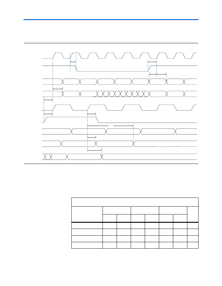
Altera Corporation
4–13
February 2005
Preliminary
Timing Model
Figure 4–1
shows the memory waveforms for the M4K timing parameters
shown in
Table 4–23
.
Figure 4–1. Dual-Port RAM Timing Microparameter Waveform
Internal timing parameters are specified on a speed grade basis
independent of device density.
Tables 4–25
through
4–28
show the
internal timing microparameters for LEs, IOEs, TriMatrix memory
structures, DSP blocks, and MultiTrack interconnects.
wrclock
wren
wraddress
data-in
reg_data-out
an-1
an
a0
a1
a2
a3
a4
a5
din-1
din
din4
din5
rdclock
a6
din6
unreg_data-out
rden
rdaddress
bn
b0
b1
b2
b3
doutn-2
doutn-1
doutn
doutn-1
doutn
dout0
t
WERESU
t
WEREH
t
DATACO1
t
DATACO2
t
DATASU
t
DATAH
t
WEREH
t
WERESU
t
WADDRSU
t
WADDRH
dout0
t
RC
Table 4–25. LE Internal Timing Microparameters (Part 1 of 2)
Symbol
-6
-7
-8
Unit
Min
Max
Min
Max
Min
Max
t
SU
29
33
37
ps
t
H
12
13
15
ps
t
CO
173
198
224
ps
t
LUT
454
522
590
ps
FPGA_cyc-html.html
4–14
Altera
Corporation
Preliminary
February 2005
Cyclone Device Handbook, Volume 1
t
CLR
129
148
167
ps
t
PRE
129
148
167
ps
t
CLKHL
1,234
1,562
1,818
ps
Table 4–26. IOE Internal Timing Microparameters
Symbol
-6
-7
-8
Unit
Min
Max
Min
Max
Min
Max
t
SU
348
400
452
ps
t
H
0
0
0
ps
t
CO
511
587
664
ps
t
PIN2COMBOUT_R
1,130
1,299
1,469
ps
t
PIN2COMBOUT_C
1,135
1,305
1,475
ps
t
COMBIN2PIN_R
2,627
3,021
3,415
ps
t
COMBIN2PIN_C
2,615
3,007
3,399
ps
t
CLR
280
322
364
ps
t
PRE
280
322
364
ps
t
CLKHL
1,234
1,562
1,818
ps
Table 4–27. M4K Block Internal Timing Microparameters (Part 1 of 2)
Symbol
-6
-7
-8
Unit
Min
Max
Min
Max
Min
Max
t
M4KRC
4,379
5,035
5,691
ps
t
M4KWC
2,910
3,346
3,783
ps
t
M4KWERESU
72
82
93
ps
t
M4KWEREH
43
49
55
ps
t
M4KBESU
72
82
93
ps
t
M4KBEH
43
49
55
ps
t
M4KDATAASU
72
82
93
ps
t
M4KDATAAH
43
49
55
ps
Table 4–25. LE Internal Timing Microparameters (Part 2 of 2)
Symbol
-6
-7
-8
Unit
Min
Max
Min
Max
Min
Max
FPGA_cyc-html.html
Altera Corporation
4–15
February 2005
Preliminary
Timing Model
External Timing Parameters
External timing parameters are specified by device density and speed
grade.
Figure 4–2
shows the timing model for bidirectional IOE pin
timing. All registers are within the IOE.
t
M4KADDRASU
72
82
93
ps
t
M4KADDRAH
43
49
55
ps
t
M4KDATABSU
72
82
93
ps
t
M4KDATABH
43
49
55
ps
t
M4KADDRBSU
72
82
93
ps
t
M4KADDRBH
43
49
55
ps
t
M4KDATACO1
621
714
807
ps
t
M4KDATACO2
4,351
5,003
5,656
ps
t
M4KCLKHL
1,234
1,562
1,818
ps
t
M4KCLR
286
328
371
ps
Table 4–28. Routing Delay Internal Timing Microparameters
Symbol
-6
-7
-8
Unit
Min
Max
Min
Max
Min
Max
t
R4
261
300
339
ps
t
C4
338
388
439
ps
t
LOCAL
244
281
318
ps
Table 4–27. M4K Block Internal Timing Microparameters (Part 2 of 2)
Symbol
-6
-7
-8
Unit
Min
Max
Min
Max
Min
Max
FPGA_cyc-html.html
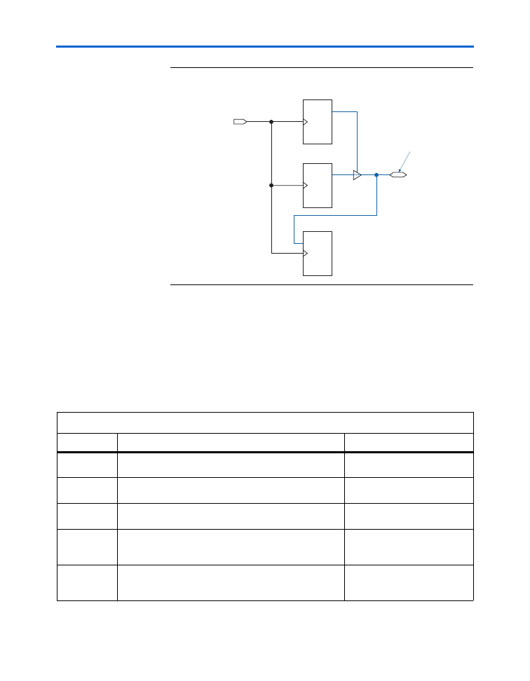
4–16
Altera
Corporation
Preliminary
February 2005
Cyclone Device Handbook, Volume 1
Figure 4–2. External Timing in Cyclone Devices
All external I/O timing parameters shown are for 3.3-V LVTTL I/O
standard with the maximum current strength and fast slew rate. For
external I/O timing using standards other than LVTTL or for different
current strengths, use the I/O standard input and output delay adders in
Tables 4–40
through
4–44
.
Table 4–29
shows the external I/O timing parameters when using global
clock networks.
PRN
CLRN
D
Q
PRN
CLRN
D
Q
PRN
CLRN
D
Q
Dedicated
Clock
Bidirectional
Pin
Output Register
Input Register
OE Register
t
XZ
t
ZX
t
INSU
t
INH
t
OUTCO
Table 4–29. Cyclone Global Clock External I/O Timing Parameters
Notes (1)
,
(2)
(Part 1 of 2)
Symbol
Parameter
Conditions
t
I N S U
Setup time for input or bidirectional pin using IOE input
register with global clock fed by
CLK
pin
t
I N H
Hold time for input or bidirectional pin using IOE input
register with global clock fed by
CLK
pin
t
O U T C O
Clock-to-output delay output or bidirectional pin using IOE
output register with global clock fed by
CLK
pin
C
LOAD
= 10 pF
t
I N S U P L L
Setup time for input or bidirectional pin using IOE input
register with global clock fed by Enhanced PLL with default
phase setting
t
I N H P L L
Hold time for input or bidirectional pin using IOE input
register with global clock fed by enhanced PLL with default
phase setting
FPGA_cyc-html.html
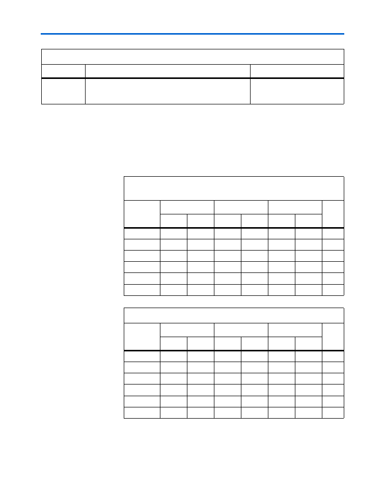
Altera Corporation
4–17
February 2005
Preliminary
Timing Model
Tables 4–30
through
4–31
show the external timing parameters on column
and row pins for EP1C3 devices.
t
O U T C O P L L
Clock-to-output delay output or bidirectional pin using IOE
output register with global clock enhanced PLL with default
phase setting
C
LOAD
= 10 pF
Notes to
Table 4–29
:
(1)
These timing parameters are sample-tested only.
(2)
These timing parameters are for IOE pins using a 3.3-V LVTTL, 24-mA setting. Designers should use the Quartus II
software to verify the external timing for any pin.
Table 4–29. Cyclone Global Clock External I/O Timing Parameters
Notes (1)
,
(2)
(Part 2 of 2)
Symbol
Parameter
Conditions
Table 4–30. EP1C3 Column Pin Global Clock External I/O Timing
Parameters
Symbol
-6 Speed Grade
-7 Speed Grade
-8 Speed Grade
Unit
Min
Max
Min
Max
Min
Max
t
I N S U
3.085
3.547
4.009
ns
t
I N H
0.000
0.000
0.000
ns
t
O U T C O
2.000
4.073
2.000
4.682
2.000
5.295
ns
t
I N S U P L L
1.795
2.063
2.332
ns
t
I N H P L L
0.000
0.000
0.000
ns
t
O U T C O P L L
0.500
2.306
0.500
2.651
0.500
2.998
ns
Table 4–31. EP1C3 Row Pin Global Clock External I/O Timing Parameters
Symbol
-6 Speed Grade
-7 Speed Grade
-8 Speed Grade
Unit
Min
Max
Min
Max
Min
Max
t
I N S U
3.157
3.630
4.103
ns
t
I N H
0.000
0.000
0.000
ns
t
O U T C O
2.000
3.984
2.000
4.580
2.000
5.180
ns
t
I N S U P L L
1.867
2.146
2.426
ns
t
I N H P L L
0.000
0.000
0.000
ns
t
O U T C O P L L
0.500
2.217
0.500
2.549
0.500
2.883
ns
FPGA_cyc-html.html
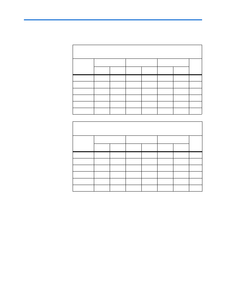
4–18
Altera
Corporation
Preliminary
February 2005
Cyclone Device Handbook, Volume 1
Tables 4–32
through
4–33
show the external timing parameters on column
and row pins for EP1C4 devices.
Table 4–32. EP1C4 Column Pin Global Clock External I/O Timing
Parameters
Note (1)
Symbol
-6 Speed Grade
-7 Speed Grade
-8 Speed Grade
Unit
Min
Max
Min
Max
Min
Max
t
I N S U
2.471
2.841
3.210
ns
t
I N H
0.000
0.000
0.000
ns
t
O U T C O
2.000
3.937
2.000
4.526
2.000
5.119
ns
t
I N S U P L L
1.471
1.690
1.910
ns
t
I N H P L L
0.000
0.000
0.000
ns
t
O U T C O P L L
0.500
2.080
0.500
2.392
0.500
2.705
ns
Table 4–33. EP1C4 Row Pin Global Clock External I/O Timing
Parameters
Note (1)
Symbol
-6 Speed Grade
-7 Speed Grade
-8 Speed Grade
Unit
Min
Max
Min
Max
Min
Max
t
I N S U
2.600
2.990
3.379
ns
t
I N H
0.000
0.000
0.000
ns
t
O U T C O
2.000
3.991
2.000
4.388
2.000
5.189
ns
t
I N S U P L L
1.300
1.494
1.689
ns
t
I N H P L L
0.000
0.000
0.000
ns
t
O U T C O P L L
0.500
2.234
0.500
2.569
0.500
2.905
ns
Note to
Tables 4–32
and
4–33
:
(1)
Contact Altera Applications for EP1C4 device timing parameters.
FPGA_cyc-html.html
Altera Corporation
4–19
February 2005
Preliminary
Timing Model
Tables 4–34
through
4–35
show the external timing parameters on column
and row pins for EP1C6 devices.
Tables 4–36
through
4–37
show the external timing parameters on column
and row pins for EP1C12 devices.
Table 4–34. EP1C6 Column Pin Global Clock External I/O Timing Parameters
Symbol
-6 Speed Grade
-7 Speed Grade
-8 Speed Grade
Unit
Min
Max
Min
Max
Min
Max
t
I N S U
2.691
3.094
3.496
ns
t
I N H
0.000
0.000
0.000
ns
t
O U T C O
2.000
3.917
2.000
4.503
2.000
5.093
ns
t
I N S U P L L
1.513
1.739
1.964
ns
t
I N H P L L
0.000
0.000
0.000
ns
t
O U T C O P L L
0.500
2.038
0.500
2.343
0.500
2.651
ns
Table 4–35. EP1C6 Row Pin Global Clock External I/O Timing Parameters
Symbol
-6 Speed Grade
-7 Speed Grade
-8 Speed Grade
Unit
Min
Max
Min
Max
Min
Max
t
I N S U
2.774
3.190
3.605
ns
t
I N H
0.000
0.000
0.000
ns
t
O U T C O
2.000
3.817
2.000
4.388
2.000
4.963
ns
t
I N S U P L L
1.596
1.835
2.073
ns
t
I N H P L L
0.000
0.000
0.000
ns
t
O U T C O P L L
0.500
1.938
0.500
2.228
0.500
2.521
ns
Table 4–36. EP1C12 Column Pin Global Clock External I/O Timing
Parameters (Part 1 of 2)
Symbol
-6 Speed Grade
-7 Speed Grade
-8 Speed Grade
Unit
Min
Max
Min
Max
Min
Max
t
I N S U
2.510
2.885
3.259
ns
t
I N H
0.000
0.000
0.000
ns
tO
U T C O
2.000
3.798
2.000
4.367
2.000
4.940
ns
t
I N S U P L L
1.588
1.824
2.061
ns
FPGA_cyc-html.html
4–20
Altera
Corporation
Preliminary
February 2005
Cyclone Device Handbook, Volume 1
Tables 4–38
through
4–39
show the external timing parameters on column
and row pins for EP1C20 devices.
t
I N H P L L
0.000
0.000
0.000
ns
t
O U T C O P L L
0.500
1.663
0.500
1.913
0.500
2.164
ns
Table 4–37. EP1C12 Row Pin Global Clock External I/O Timing Parameters
Symbol
-6 Speed Grade
-7 Speed Grade
-8 Speed Grade
Unit
Min
Max
Min
Max
Min
Max
t
I N S U
2.620
3.012
3.404
ns
t
I N H
0.000
0.000
0.000
ns
t
O U T C O
2.000
3.671
2.000
4.221
2.000
4.774
ns
t
I N S U P L L
1.698
1.951
2.206
ns
t
I N H P L L
0.000
0.000
0.000
ns
t
O U T C O P L L
0.500
1.536
0.500
1.767
0.500
1.998
ns
Table 4–38. EP1C20 Column Pin Global Clock External I/O Timing
Parameters
Symbol
-6 Speed Grade
-7 Speed Grade
-8 Speed Grade
Unit
Min
Max
Min
Max
Min
Max
t
I N S U
2.417
2.779
3.140
ns
t
I N H
0.000
0.000
0.000
ns
t
O U T C O
2.000
3.724
2.000
4.282
2.000
4.843
ns
t
I N S U P L L
1.417
1.629
1.840
ns
t
I N H P L L
0.000
0.000
0.000
ns
t
O U T C O P L L
0.500
1.667
0.500
1.917
0.500
2.169
ns
Table 4–36. EP1C12 Column Pin Global Clock External I/O Timing
Parameters (Part 2 of 2)
Symbol
-6 Speed Grade
-7 Speed Grade
-8 Speed Grade
Unit
Min
Max
Min
Max
Min
Max
FPGA_cyc-html.html
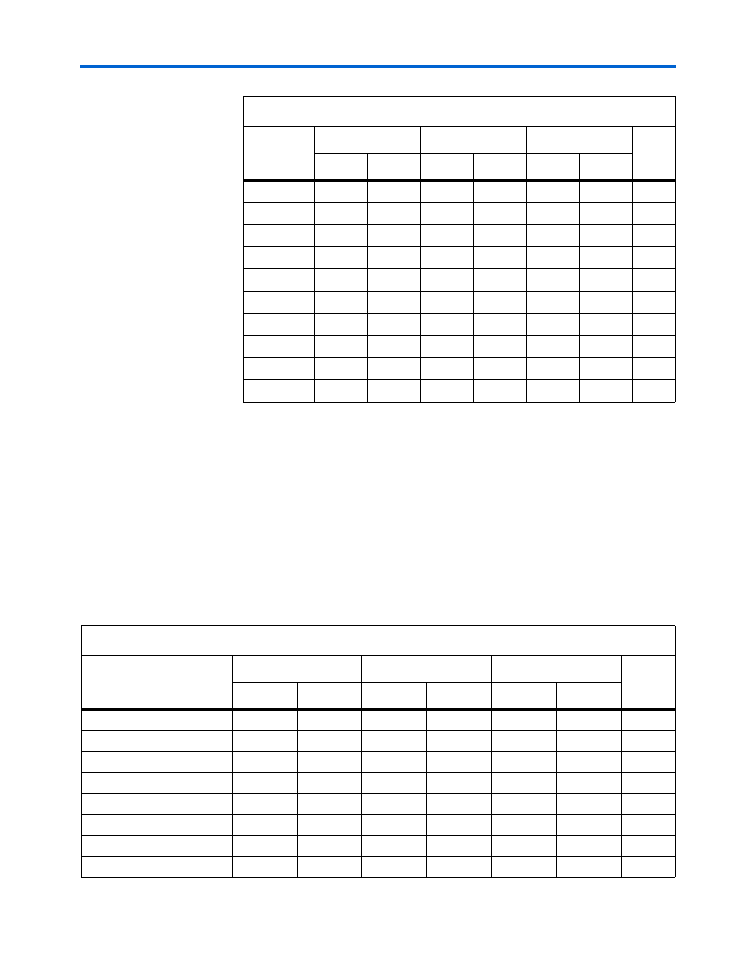
Altera Corporation
4–21
February 2005
Preliminary
Timing Model
External I/O Delay Parameters
External I/O delay timing parameters for I/O standard input and output
adders and programmable input and output delays are specified by
speed grade independent of device density.
Tables 4–40
through
4–45
show the adder delays associated with column
and row I/O pins for all packages. If an I/O standard is selected other
than LVTTL 24 mA with a fast slew rate, add the selected delay to the
external t
CO
and t
SU
I/O parameters shown in
Tables 4–25
through
4–28
.
Table 4–39. EP1C20 Row Pin Global Clock External I/O Timing Parameters
Symbol
-6 Speed Grade
-7 Speed Grade
-8 Speed Grade
Unit
Min
Max
Min
Max
Min
Max
t
I N S U
2.417
2.779
3.140
ns
t
I N H
0.000
0.000
0.000
ns
t
O U T C O
2.000
3.724
2.000
4.282
2.000
4.843
ns
t
X Z
3.645
4.191
4.740
ns
t
Z X
3.645
4.191
4.740
ns
t
I N S U P L L
1.417
1.629
1.840
ns
t
I N H P L L
0.000
0.000
0.000
ns
t
O U T C O P L L
0.500
1.667
0.500
1.917
0.500
2.169
ns
t
X Z P L L
1.588
1.826
2.066
ns
t
Z X P L L
1.588
1.826
2.066
ns
Table 4–40. Cyclone I/O Standard Column Pin Input Delay Adders (Part 1 of 2)
I/O Standard
-6 Speed Grade
-7 Speed Grade
-8 Speed Grade
Unit
Min
Max
Min
Max
Min
Max
LVCMOS
0
0
0
ps
3.3-V LVTTL
0
0
0
ps
2.5-V LVTTL
27
31
35
ps
1.8-V LVTTL
182
209
236
ps
1.5-V LVTTL
278
319
361
ps
SSTL-3 class I
−
250
−
288
−
325
ps
SSTL-3 class II
−
250
−
288
−
325
ps
SSTL-2 class I
−
278
−
320
−
362
ps
FPGA_cyc-html.html
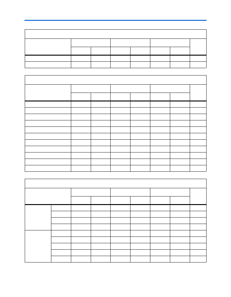
4–22
Altera
Corporation
Preliminary
February 2005
Cyclone Device Handbook, Volume 1
SSTL-2 class II
−
278
−
320
−
362
ps
LVDS
−
261
−
301
−
340
ps
Table 4–41. Cyclone I/O Standard Row Pin Input Delay Adders
I/O Standard
-6 Speed Grade
-7 Speed Grade
-8 Speed Grade
Unit
Min
Max
Min
Max
Min
Max
LVCMOS
0
0
0
ps
3.3-V LVTTL
0
0
0
ps
2.5-V LVTTL
27
31
35
ps
1.8-V LVTTL
182
209
236
ps
1.5-V LVTTL
278
319
361
ps
3.3-V PCI
(1)
0
0
0
ps
SSTL-3 class I
−
250
−
288
−
325
ps
SSTL-3 class II
−
250
−
288
−
325
ps
SSTL-2 class I
−
278
−
320
−
362
ps
SSTL-2 class II
−
278
−
320
−
362
ps
LVDS
−
261
−
301
−
340
ps
Table 4–42. Cyclone I/O Standard Output Delay Adders for Fast Slew Rate on Column Pins (Part 1 of 2)
Standard
-6 Speed Grade
-7 Speed Grade
-8 Speed Grade
Unit
Min
Max
Min
Max
Min
Max
LVCMOS
2 mA
0
0
0
ps
4 mA
−
489
−
563
−
636
ps
8 mA
−
855
−
984
−
1,112
ps
12 mA
−
993
−
1,142
−
1,291
ps
3.3-V LVTTL
4 mA
0
0
0
ps
8 mA
−
347
−
400
−
452
ps
12 mA
−
858
−
987
−
1,116
ps
16 mA
−
819
−
942
−
1,065
ps
24 mA
−
993
−
1,142
−
1,291
ps
Table 4–40. Cyclone I/O Standard Column Pin Input Delay Adders (Part 2 of 2)
I/O Standard
-6 Speed Grade
-7 Speed Grade
-8 Speed Grade
Unit
Min
Max
Min
Max
Min
Max
FPGA_cyc-html.html
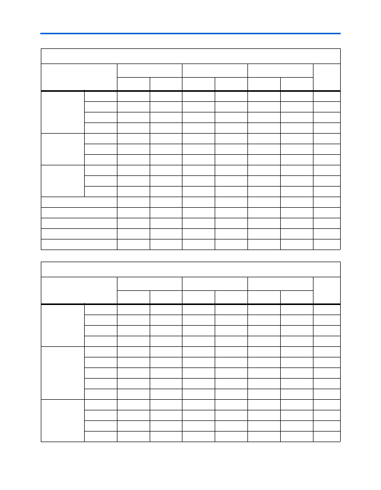
Altera Corporation
4–23
February 2005
Preliminary
Timing Model
2.5-V LVTTL
2 mA
329
378
427
ps
8 mA
−
661
−
761
−
860
ps
12 mA
−
655
−
754
−
852
ps
16 mA
−
795
−
915
−
1034
ps
1.8-V LVTTL
2 mA
4
4
5
ps
8 mA
−
208
−
240
−
271
ps
12 mA
−
208
−
240
−
271
ps
1.5-V LVTTL
2 mA
2,288
2,631
2,974
ps
4 mA
608
699
790
ps
8 mA
292
335
379
ps
SSTL-3 class I
−
410
−
472
−
533
ps
SSTL-3 class II
−
811
−
933
−
1,055
ps
SSTL-2 class I
−
485
−
558
−
631
ps
SSTL-2 class II
−
758
−
872
−
986
ps
LVDS
−998
−1,148
−
1,298
ps
Table 4–43. Cyclone I/O Standard Output Delay Adders for Fast Slew Rate on Row Pins (Part 1 of 2)
Standard
-6 Speed Grade
-7 Speed Grade
-8 Speed Grade
Unit
Min
Max
Min
Max
Min
Max
LVCMOS
2 mA
0
0
0
ps
4 mA
−
489
−
563
−
636
ps
8 mA
−
855
−
984
−
1,112
ps
12 mA
−
993
−
1,142
−
1,291
ps
3.3-V LVTTL
4 mA
0
0
0
ps
8 mA
−
347
−
400
−
452
ps
12 mA
-858
−
987
−
1,116
ps
16 mA
−
819
−
942
−
1,065
ps
24 mA
−
993
−
1,142
−
1,291
ps
2.5-V LVTTL
2 mA
329
378
427
ps
8 mA
−
661
−
761
−
860
ps
12 mA
−
655
−
754
−
852
ps
16 mA
−
795
−
915
−
1,034
ps
Table 4–42. Cyclone I/O Standard Output Delay Adders for Fast Slew Rate on Column Pins (Part 2 of 2)
Standard
-6 Speed Grade
-7 Speed Grade
-8 Speed Grade
Unit
Min
Max
Min
Max
Min
Max
FPGA_cyc-html.html
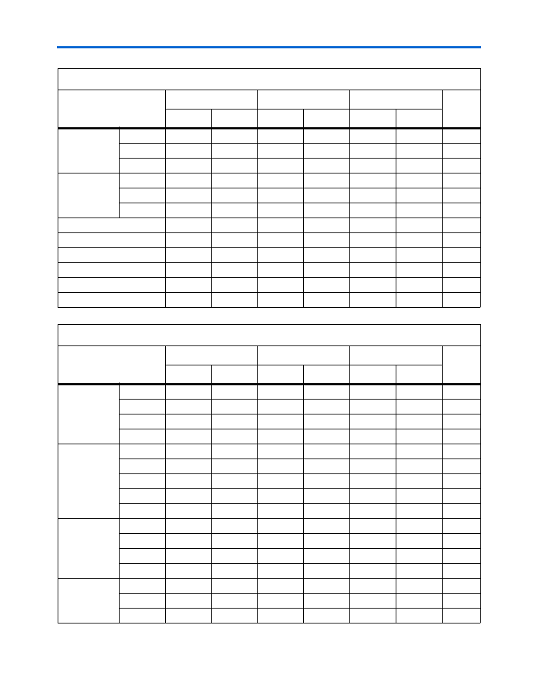
4–24
Altera
Corporation
Preliminary
February 2005
Cyclone Device Handbook, Volume 1
1.8-V LVTTL
2 mA
1,290
1,483
1,677
ps
8 mA
4
4
5
ps
12 mA
−
208
−
240
−
271
ps
1.5-V LVTTL
2 mA
2,288
2,631
2,974
ps
4 mA
608
699
790
ps
8 mA
292
335
379
ps
3.3-V PCI
(1)
−
877
−
1,009
−
1,141
ps
SSTL-3 class I
−
410
−
472
−
533
ps
SSTL-3 class II
−
811
−
933
−
1,055
ps
SSTL-2 class I
−
485
−
558
−
631
ps
SSTL-2 class II
−
758
−
872
−
986
ps
LVDS
−
998
−
1,148
−
1,298
ps
Table 4–44. Cyclone I/O Standard Output Delay Adders for Slow Slew Rate on Column Pins (Part 1 of 2)
I/O Standard
-6 Speed Grade
-7 Speed Grade
-8 Speed Grade
Unit
Min
Max
Min
Max
Min
Max
LVCMOS
2 mA
1,800
2,070
2,340
ps
4 mA
1,311
1,507
1,704
ps
8 mA
945
1,086
1,228
ps
12 mA
807
928
1,049
ps
3.3-V LVTTL
4 mA
1,831
2,105
2,380
ps
8 mA
1,484
1,705
1,928
ps
12 mA
973
1,118
1,264
ps
16 mA
1,012
1,163
1,315
ps
24 mA
838
963
1,089
ps
2.5-V LVTTL
2 mA
2,747
3,158
3,570
ps
8 mA
1,757
2,019
2,283
ps
12 mA
1,763
2,026
2,291
ps
16 mA
1,623
1,865
2,109
ps
1.8-V LVTTL
2 mA
5,506
6,331
7,157
ps
8 mA
4,220
4,852
5,485
ps
12 mA
4,008
4,608
5,209
ps
Table 4–43. Cyclone I/O Standard Output Delay Adders for Fast Slew Rate on Row Pins (Part 2 of 2)
Standard
-6 Speed Grade
-7 Speed Grade
-8 Speed Grade
Unit
Min
Max
Min
Max
Min
Max
FPGA_cyc-html.html
Altera Corporation
4–25
February 2005
Preliminary
Timing Model
1.5-V LVTTL
2 mA
6,789
7,807
8,825
ps
4 mA
5,109
5,875
6,641
ps
8 mA
4,793
5,511
6,230
ps
SSTL-3 class I
1,390
1,598
1,807
ps
SSTL-3 class II
989
1,137
1,285
ps
SSTL-2 class I
1,965
2,259
2,554
ps
SSTL-2 class II
1,692
1,945
2,199
ps
LVDS
802
922
1,042
ps
Table 4–45. Cyclone I/O Standard Output Delay Adders for Slow Slew Rate on Row Pins (Part 1 of 2)
I/O Standard
-6 Speed Grade
-7 Speed Grade
-8 Speed Grade
Unit
Min
Max
Min
Max
Min
Max
LVCMOS
2 mA
1,800
2,070
2,340
ps
4 mA
1,311
1,507
1,704
ps
8 mA
945
1,086
1,228
ps
12 mA
807
928
1,049
ps
3.3-V LVTTL
4 mA
1,831
2,105
2,380
ps
8 mA
1,484
1,705
1,928
ps
12 mA
973
1,118
1,264
ps
16 mA
1,012
1,163
1,315
ps
24 mA
838
963
1,089
ps
2.5-V LVTTL
2 mA
2,747
3,158
3,570
ps
8 mA
1,757
2,019
2,283
ps
12 mA
1,763
2,026
2,291
ps
16 mA
1,623
1,865
2,109
ps
1.8-V LVTTL
2 mA
5,506
6,331
7,157
ps
8 mA
4,220
4,852
5,485
ps
12 mA
4,008
4,608
5,209
ps
1.5-V LVTTL
2 mA
6,789
7,807
8,825
ps
4 mA
5,109
5,875
6,641
ps
8 mA
4,793
5,511
6,230
ps
3.3-V PCI
923
1,061
1,199
ps
Table 4–44. Cyclone I/O Standard Output Delay Adders for Slow Slew Rate on Column Pins (Part 2 of 2)
I/O Standard
-6 Speed Grade
-7 Speed Grade
-8 Speed Grade
Unit
Min
Max
Min
Max
Min
Max
FPGA_cyc-html.html
4–26
Altera
Corporation
Preliminary
February 2005
Cyclone Device Handbook, Volume 1
Tables 4–46
through
4–47
show the adder delays for the IOE
programmable delays. These delays are controlled with the Quartus II
software options listed in the Parameter column.
SSTL-3 class I
1,390
1,598
1,807
ps
SSTL-3 class II
989
1,137
1,285
ps
SSTL-2 class I
1,965
2,259
2,554
ps
SSTL-2 class II
1,692
1,945
2,199
ps
LVDS
802
922
1,042
ps
Note to
Tables 4–40
through
4–45
:
(1)
EP1C3 devices do not support the PCI I/O standard.
Table 4–45. Cyclone I/O Standard Output Delay Adders for Slow Slew Rate on Row Pins (Part 2 of 2)
I/O Standard
-6 Speed Grade
-7 Speed Grade
-8 Speed Grade
Unit
Min
Max
Min
Max
Min
Max
Table 4–46. Cyclone IOE Programmable Delays on Column Pins
Parameter
Setting
-6 Speed Grade
-7 Speed Grade
-8 Speed Grade
Unit
Min
Max
Min
Max
Min
Max
Decrease input delay to
internal cells
Off
3,057
3,515
3,974
ps
Small
2,639
3,034
3,430
ps
Medium
2,212
2,543
2,875
ps
Large
155
178
201
ps
On
155
178
201
ps
Decrease input delay to
input register
Off
3,057
3,515
3,974
ps
On
0
0
0
ps
Increase delay to output
pin
Off
0
0
0
ps
On
552
634
717
ps
FPGA_cyc-html.html
Altera Corporation
4–27
February 2005
Preliminary
Timing Model
Maximum Input & Output Clock Rates
Tables 4–48
and
4–49
show the maximum input clock rate for column and
row pins in Cyclone devices.
Table 4–47. Cyclone IOE Programmable Delays on Row Pins
Parameter
Setting
-6 Speed Grade
-7 Speed Grade
-8 Speed Grade
Unit
Min
Max
Min
Max
Min
Max
Decrease input delay to
internal cells
Off
3,057
3,515
3,974
ps
Small
2,639
3,034
3,430
ps
Medium
2,212
2,543
2,875
ps
Large
154
177
200
ps
On
154
177
200
ps
Decrease input delay to input
register
Off
3,057
3,515
3,974
ps
On
0
0
0
ps
Increase delay to output pin
Off
0
0
0
ps
On
556
639
722
ps
Note 1:
Table 4–47
(1)
EPC1C3 devices do not support the PCI I/O standard
Table 4–48. Cyclone Maximum Input Clock Rate for Column Pins
I/O Standard
-6 Speed
Grade
-7 Speed
Grade
-8 Speed
Grade
Unit
LVTTL
464
428
387
MHz
2.5 V
392
302
207
MHz
1.8 V
387
311
252
MHz
1.5 V
387
320
243
MHz
LVCMOS
405
374
333
MHz
SSTL-3 class I
405
356
293
MHz
SSTL-3 class II
414
365
302
MHz
SSTL-2 class I
464
428
396
MHz
SSTL-2 class II
473
432
396
MHz
LVDS
567
549
531
MHz
FPGA_cyc-html.html
4–28
Altera
Corporation
Preliminary
February 2005
Cyclone Device Handbook, Volume 1
Tables 4–50
and
4–51
show the maximum output clock rate for column
and row pins in Cyclone devices.
Table 4–49. Cyclone Maximum Input Clock Rate for Row Pins
I/O Standard
-6 Speed
Grade
-7 Speed
Grade
-8 Speed
Grade
Unit
LVTTL
464
428
387
MHz
2.5 V
392
302
207
MHz
1.8 V
387
311
252
MHz
1.5 V
387
320
243
MHz
LVCMOS
405
374
333
MHz
SSTL-3 class I
405
356
293
MHz
SSTL-3 class II
414
365
302
MHz
SSTL-2 class I
464
428
396
MHz
SSTL-2 class II
473
432
396
MHz
3.3-V PCI
(1)
464
428
387
MHz
LVDS
567
549
531
MHz
Note to
Tables 4–48
through
4–49
:
(1)
EP1C3 devices do not support the PCI I/O standard. These parameters are only
available on row I/O pins.
Table 4–50. Cyclone Maximum Output Clock Rate for Column Pins
I/O Standard
-6 Speed
Grade
-7 Speed
Grade
-8 Speed
Grade
Unit
LVTTL
304
304
304
MHz
2.5 V
220
220
220
MHz
1.8 V
213
213
213
MHz
1.5 V
166
166
166
MHz
LVCMOS
304
304
304
MHz
SSTL-3 class I
100
100
100
MHz
SSTL-3 class II
100
100
100
MHz
SSTL-2 class I
134
134
134
MHz
SSTL-2 class II
134
134
134
MHz
LVDS
320
320
275
MHz
Note:
Table 4–50
(1)
EP1C3 devices do not support the PCI I/O standard.
FPGA_cyc-html.html
Altera Corporation
4–29
February 2005
Preliminary
Timing Model
PLL Timing
Table 4–52
describes the Cyclone FPGA PLL specifications.
Table 4–51. Cyclone Maximum Output Clock Rate for Row Pins
I/O Standard
-6 Speed
Grade
-7 Speed
Grade
-8 Speed
Grade
Unit
LVTTL
296
285
273
MHz
2.5 V
381
366
349
MHz
1.8 V
286
277
267
MHz
1.5 V
219
208
195
MHz
LVCMOS
367
356
343
MHz
SSTL-3 class I
169
166
162
MHz
SSTL-3 class II
160
151
146
MHz
SSTL-2 class I
160
151
142
MHz
SSTL-2 class II
131
123
115
MHz
3.3-V PCI
(1)
66
66
66
MHz
LVDS
328
303
275
MHz
Note to
Tables 4–50
through
4–51
:
(1)
EP1C3 devices do not support the PCI I/O standard. These parameters are only
available on row I/O pins.
Table 4–52. Cyclone PLL Specifications
Note (1)
(Part 1 of 2)
Symbol
Parameter
Min
Max
Unit
f
IN
Input frequency (-6 speed
grade)
15.625
464
MHz
Input frequency (-7 speed
grade)
15.625
428
MHz
Input frequency (-8 speed
grade)
15.625
387
MHz
f
IN
DUTY
Input clock duty cycle
40.00
60
%
t
IN
JITTER
Input clock period jitter
±
200
ps
f
OUT_EXT
(external PLL
clock output)
PLL output frequency
(-6 speed grade)
15.625
320
MHz
PLL output frequency
(-7 speed grade)
15.625
320
MHz
PLL output frequency
(-8 speed grade)
15.625
275
MHz
FPGA_cyc-html.html
4–30
Altera
Corporation
Preliminary
February 2005
Cyclone Device Handbook, Volume 1
f
OUT
(to global clock)
PLL output frequency
(-6 speed grade)
15.625
405
MHz
PLL output frequency
(-7 speed grade)
15.625
320
MHz
PLL output frequency
(-8 speed grade)
15.625
275
MHz
t
OUT
DUTY
Duty cycle for external clock
output (when set to 50
%
)
45.00
55
%
t
JITTER
(2)
Period jitter for external clock
output
±300
(3)
ps
t
LOCK
(4)
Time required to lock from end
of device configuration
10.00
100
µ
s
f
VCO
PLL internal VCO operating
range
500.00
1,000
MHz
M
Counter values
2 to 32
integer
N, G0, G1, E
Counter values
1
32
integer
Notes to
Table 4–52
:
(1)
These numbers are preliminary and pending silicon characterization.
(2)
The t
JITTER
specification for the
PLL[2..1]_OUT
pins are dependent on the I/O pins in its V
CCIO
bank, how many
of them are switching outputs, how much they toggle, and whether or not they use programmable current strength
or slow slew rate.
(3)
f
OUT
≥
100 MHz. When the PLL external clock output frequency (f
OUT
) is smaller than 100 MHz, the jitter
specification is 60 mUI.
(4)
f
IN/N
must be greater than 200 MHz to ensure correct lock circuit operation below –20 C.
Table 4–52. Cyclone PLL Specifications
Note (1)
(Part 2 of 2)
Symbol
Parameter
Min
Max
Unit
FPGA_cyc-html.html
Altera Corporation
5–1
February 2005
Preliminary
5. Reference & Ordering
Information
Software
Cyclone devices are supported by the Altera Quartus
®
II design software,
which provides a comprehensive environment for system-on-a-
programmable-chip (SOPC) design. The Quartus II software includes
HDL and schematic design entry, compilation and logic synthesis, full
simulation and advanced timing analysis, SignalTap II logic analysis, and
device configuration. See the Design Software Selector Guide for more
details on the Quartus II software features.
The Quartus II software supports the Windows 2000/NT/98, Sun Solaris,
Linux Red Hat v7.1 and HP-UX operating systems. It also supports
seamless integration with industry-leading EDA tools through the
NativeLink
®
interface.
Device Pin-Outs
Device pin-outs for Cyclone devices are available on the Altera web site
(
www.altera.com
) and in the
Cyclone FPGA Device Handbook
.
Ordering
Information
Figure 5–1
describes the ordering codes for Cyclone devices. For more
information on a specific package, refer to
Chapter 6, Package
Information for Cyclone Devices
.
Figure 5–1. Cyclone Device Packaging Ordering Information
Device Type
Package Type
6, 7, or 8 , with 6 bein
g
the fastest
Number of pins for a particular packa
g
e
ES:
T:
Q:
F:
Thin quad flat pack (TQFP)
Plastic quad flat pack (PQFP)
FineLine BGA
EP1C: Cyclone
3
4
6
12
20
C:
I:
Commercial temperature (t
J
= 0
˚
C to 85
˚
C)
Industrial temperature (t
J
= -40
˚
C to 100
˚
C)
Optional Suffix
Family Signature
Operating Temperature
Speed Grade
Pin Count
En
g
ineerin
g
sample
7
EP1C
20
C
400
F
ES
Indicates specific device options or
shipment method.
N: Lead free devices
C51005-1.1
FPGA_cyc-html.html

5–2
Altera
Corporation
Preliminary
February 2005
Cyclone Device Handbook, Volume 1
