ETALDOC 770/3
Page 1 of 5
April 2005
PRODUCT DATA SHEET
LOW DISTORTION
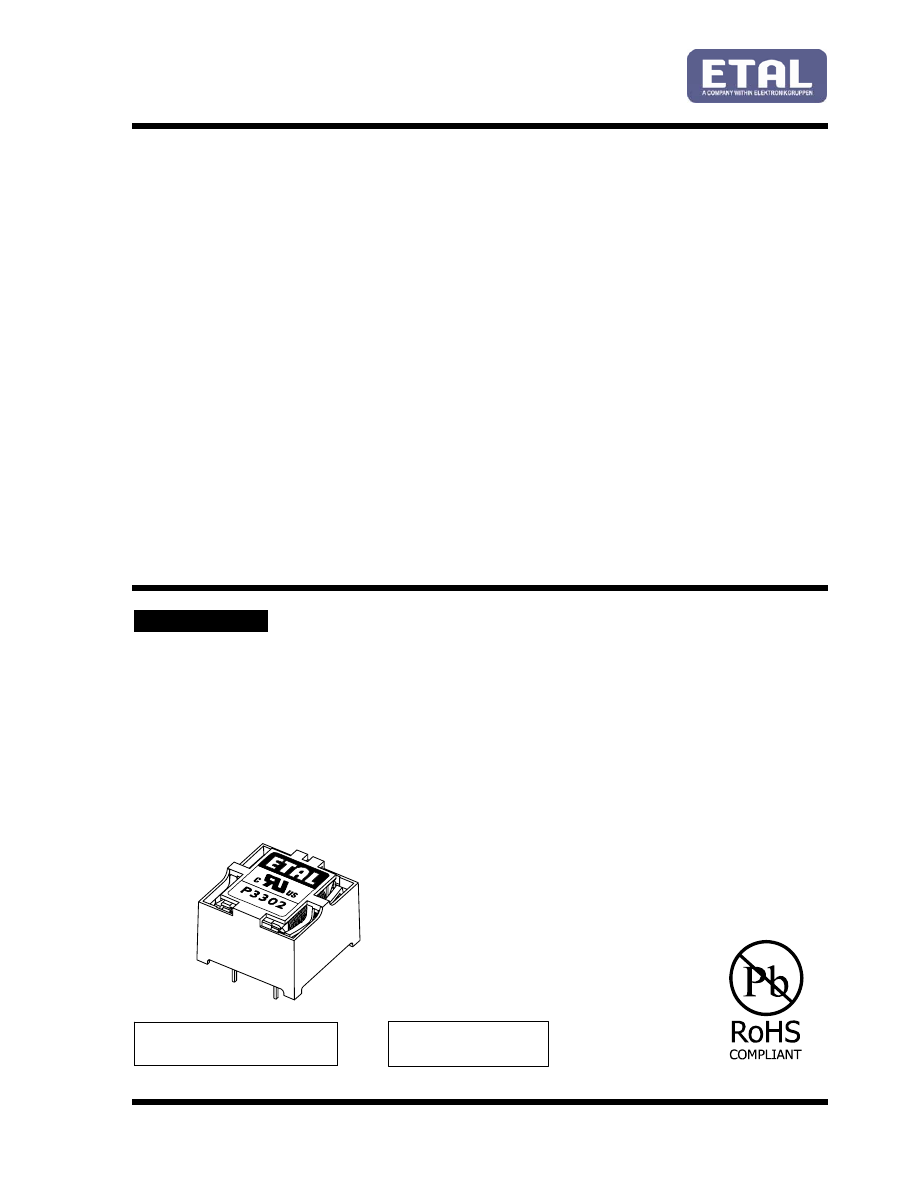
P3302
LINE MATCHING TRANSFORMER
Features
Applications
∗
Lead-free (Pb-free)
∗
V.90 and V.92 Modems
∗
RoHS compliant
∗
V.34 Modems
∗
Low Distortion
∗
12.6mm (0.5”) Seated Height
∗
IEC 60950 and UL 60950 Certified
∗
UL Recognized Component
∗
Environmentally tested to IEC 68
∗
CERT reliability tested
∗
Excellent Frequency Response
∗
High Thermal Stability
∗
Electrical substitute for XM-1025, 2802-B,
and 671-8079
DESCRIPTION
P3302 is intended for V.90 and V.92 (56kbps)
modems and other high-speed applications where
ultra-low distortion at moderate power levels and
very low voiceband frequencies is required at a
most competitive price.
P3302 is offered as a more compact internationally
safety approved substitute for XM-1025, 2802-B
and 671-8079 in existing circuits without changes
to matching components.
P3302 uses patented design and construction
methods to achieve excellent signal performance
and safety isolation to international standards.
P3302 is certified to IEC 60950 and UL 60950.
P3355 is a UL Recognized Component and is
supported by an IEC CB Test Certificate. The
part is completely lead-free, compliant with RoHS
Directive 2002/95/EC, and suitable for lead-free
and conventional processing.
P3302 has been subjected to relevant
environmental testing according to IEC 68 and
Combined Environmental Reliability Testing
(CERT) beyond normal operational levels and
passed all tests, remaining fully functional.
FOR NEW DESIGNS
P3356 IS RECOMMENDED
Patented
P3302
ETALDOC 770/3
Page 2 of 5
April 2005
SPECIFICATIONS
Electrical
At T = 25ºC and as reference circuit Fig. 2 unless otherwise stated.
Parameter Conditions
Min
Typ
Max
Units
Insertion Loss
f = 2kHz, R
L
= 600
Ω
- 2.0 - dB
Frequency Response
LF -3dB cutoff
HF -3dB cutoff
100Hz – 4kHz
-
-
-
10
30
-
-
-
±
0.1
Hz
kHz
dB
Return Loss
200Hz – 4kHz
26
30
-
dB
Third Harmonic
Distortion
(1)
150Hz -3dBm in line
-
-
-74
dBm
Voltage Isolation
(2)
50Hz
DC
2.12
3.0
-
-
-
-
kVrms
kV
Operating Range:
Functional
Storage
0
-40
-
-
+70
+85
ºC
ºC
Lumped equivalent circuit parameters as Fig. 1
DC resistance
(3)
, R
DCP
R
DCS
Primary
Secondary
126
130
-
-
154
160
Ω
Ω
Leakage inductance,
Δ
L
3.6
-
5.4
mH
Shunt inductance, Lp
200Hz 1V
8 18 - H
Shunt loss, Rp
200Hz 1V
16 19
-
k
Ω
Notes:
1. Third harmonic typically exceeds other
harmonics by 10dB.
2. Components are 100% tested at 3.25kVDC.
3. Caution: do not pass DC through windings.
Telephone line current must be diverted using
semiconductor line hold circuit or choke.
4. At signal levels greater than 100mV, Lp will
increase and Rp will decrease slightly but the
effect is usually favourable to the return loss
characteristic.
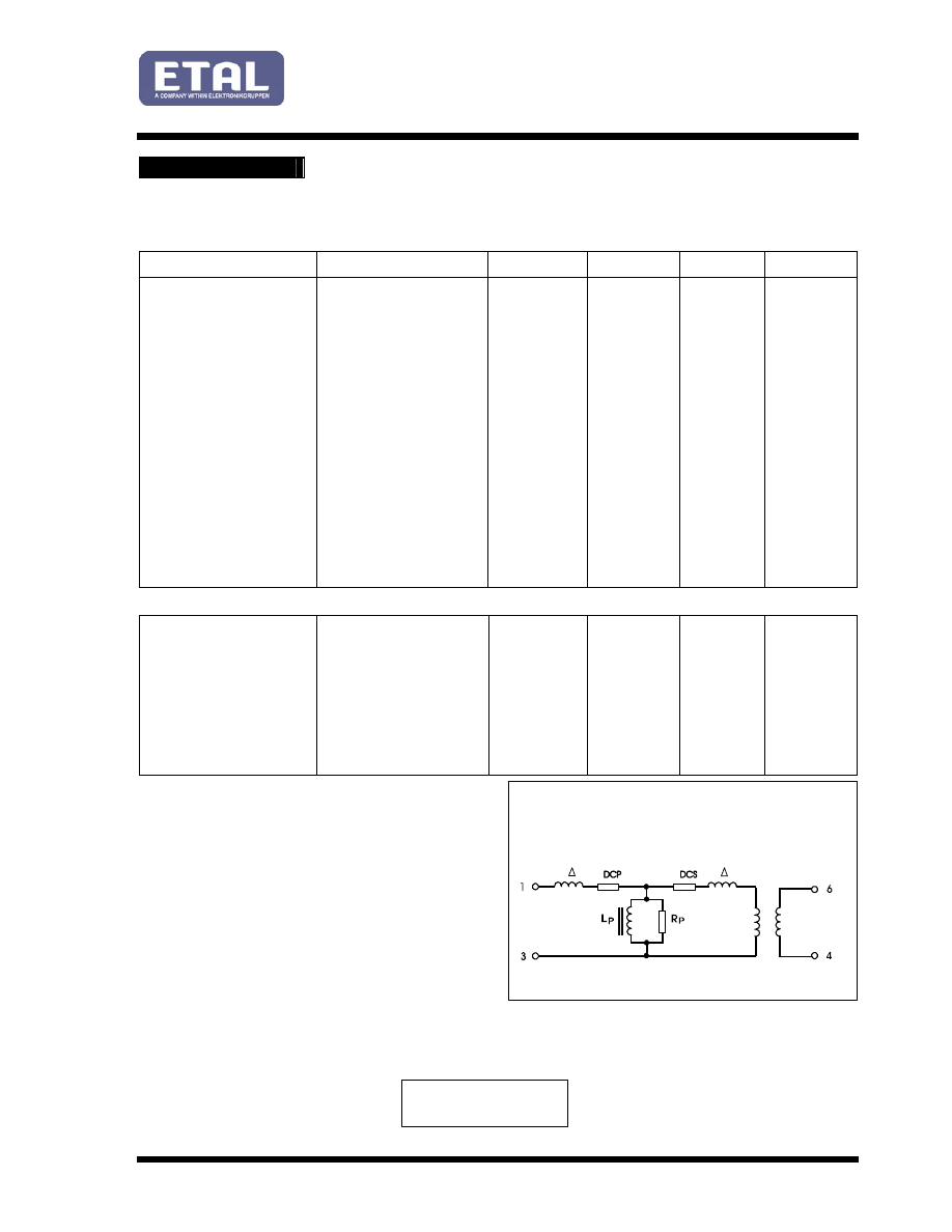
Equivalent Circuit
Fig. 1
IDEAL
1:1
½ L
½ L
R
R
Patented
P3302
ETALDOC 770/3
Page 3 of 5
April 2005
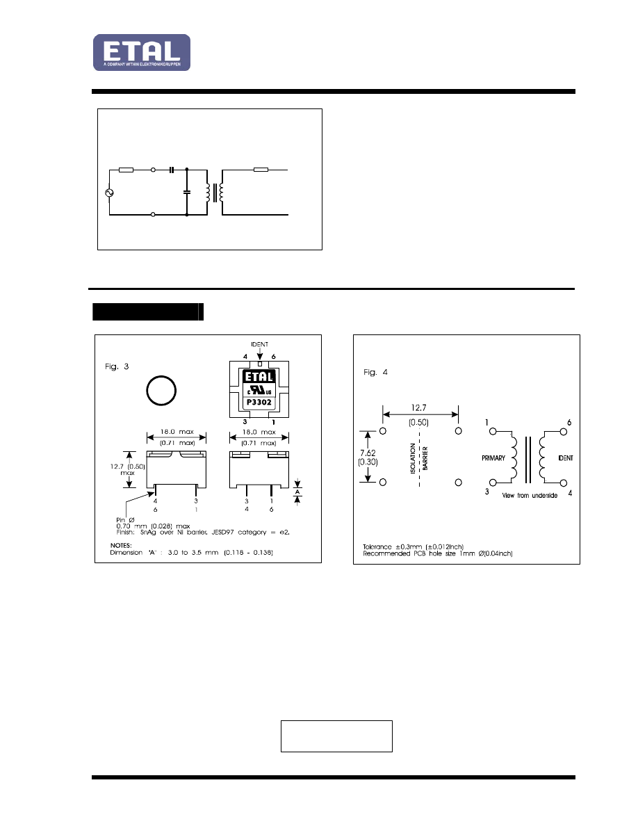
CONSTRUCTION
Dimensions shown are in millimetres (inches).
Geometric centres of outline and pin grid coincide within a tolerance circle of 0.6mmØ.
Windings may be used interchangeably as primary or secondary.
Total weight typically 6.7g.
Patented
10nF
μ
22 F
600 Reference Circuit
Ω
Fig. 2
LINE
600
300*
* Increase to 430 to improve RX loss.
Return loss > 20dB 200Hz - 4kHz
TXA2
TXA1
Connections
Dimensions
e
2
P3302
ETALDOC 770/3
Page 4 of 5
April 2005
ENVIRONMENTAL TESTING
Reliability testing to IEC 68
Tested to clauses of IEC 68 and compliant with all functional and safety requirements following exposure as follows:
Test description IEC 68 reference
Test details
Result
Robustness of
terminations
68-2-21 Test Ua
1
68-2-21 Test Ua
2
Tensile 5N pull
Thrust 1N push
No impairment
No pin detachment or distortion
Solderability
68-2-20 Test Ta Method 1 Solder bath 235ºC 2s
Resistance to
soldering heat
68-2-20 Test Tb Method 1A
68-2-20 Test Tb Method 2
Solder bath 260ºC 10s
Soldering iron 350ºC 5s
No impairment
Finish smooth, bright and even
Vibration
68-2-6 Test Fc
Sweep 10-55-10Hz in 1 minute
Amplitude 1.5mm pk-pk
Duration 2h per axis, 3 axes
No impairment
Shock 68-2-27
Test
Ea Peak acceleration 1000m/s
2
Duration of pulse 6ms
3 shocks each direction on 3 axes
No impairment
Cold
68-2-1 Test Ab
-25ºC 16h
Recovery to ambient 1-2h
No impairment
Dry heat
68-2-2 Test Bb
125ºC 16h
Recovery to ambient 1-2h
No impairment
Damp heat
68-2-3 Test Ca
40ºC 4 days, RH 93%
Recovery to ambient 1-2h
No impairment
Change of
temperature
68-2-14 Test Na
T
A
–25ºC
T
B
+85ºC
t
1
30 min
2 min
≤
t
2
≤
3 min
Recovery to ambient 1-2h
5 cycles
No impairment
Combined Environmental Reliability Testing (CERT)
Components step stressed at increasing levels of severity using combined stresses to detect potential
weaknesses.
Results are shown for highest levels of stress tested. Compliant with all functional and safety tests following
exposure as follows:
Test description
Test details
Duration
Result
Storage Test
Thermal cycling -30ºC to +100ºC at
11ºC/min
6mm pk 2-9Hz at 1 octave/min
20m/s
2
9-200Hz
20 mins per
plane
No impairment
Transportation Test Thermal cycling -65ºC to +80ºC
Random vibration 10-200Hz and
200-2000Hz at 57m/s
2
RMS
2 hours per
plane
No impairment
P3302
ETALDOC 770/3
Page 5 of 5
April 2005
SAFETY
ABSOLUTE MAXIMUM RATINGS
(Ratings of components independent of circuit).
Constructed in accordance with IEC
60950-1,
EN
60950-1 and UL
60950-1, supplementary
insulation, 250Vrms maximum working voltage,
flammability class V-0.
There are no special installation requirements
(beyond attending to usual PCB track separations)
since the integral cover provides supplementary
insulation from its external faces to internal core
and windings.
Short term isolation voltage (1s)
DC current
Storage temperature
Lead temperature, 10s
2.12kVrms,
3.0 kVDC
100
μ
A
-40ºC to
+85ºC
260ºC
CERTIFICATION
INTELLECTUAL PROPERTY RIGHTS
Certified under the IEC
CB scheme (Certificate
DK-8570) to IEC
60950-1-2001, sub-clauses 1.5,
1.5.1, 1.5.2, 1.7.1, 2.9, 2.9.1, 2.9.2, 2.9.3, 2.10, 2.10.1,
2.10.2, 2.10.3, 2.10.3.1, 2.10.3.3, 2.10.4, 2.10.5,
2.10.5.1, 2.10.5.2, 2.10.5.4, 4.7, 4.7.1 (classV-1), 4.7.3,
4.7.3.1, 4.7.3.4, 5.2, 5.2.1, 5.2.2, 6.1.2.1 (Finland,
Norway, Sweden national deviations) for a maximum
working voltage of 250Vrms, nominal mains supply
voltage not exceeding 300Vrms and a maximum
operating temperature of 70ºC in Pollution Degree
2 environments.
Recognized under the Component Recognition
Program of Underwriters Laboratories Inc. to US and
Canadian requirements CAN/CSA C22.2
No. 60950-1-03/UL60950-1, First Edition, based on
IEC 60950-1, First Edition, maximum working voltage
180Vrms (creepage), 420V peak (clearance), Pollution
Degree 2, supplementary insulation.
UL File number E203175.
Additionally, Profec Technologies certifies all
transformers as providing voltage isolation of
2.12kVrms, 3kV DC minimum. All shipments are
supported by a certificate of conformity to current
applicable safety standards.
ETAL and P3302 are Trade Marks of Profec
Technologies Ltd.
The Trade Mark ETAL is registered at the UK
Trade Marks Registry.
Profec Technologies Ltd. is the owner of the
design right under the Copyright Designs and
Patents Act 1988 and no rights or licences are
hereby granted or implied to any third party.
P3302 design and construction are protected by
patents and registered design.
British Patent No. 2333646.
USA Patent Nos. 6, 344, 787; 6,690,254
European Patent No. 1082734
China Patent No. ZL 99806739.3
UK Registered Design No. 2077360.
French Registered Design No. 991512.
United States Registered Design 426, 815.
Mexico Registered Design 12143
Other patents and registered designs pending.
© 1998 - 2005 Profec Technologies Ltd.
Reproduction prohibited
ETAL Group Oy, Kuormatie 14, FIN-03101, Nummela
Telephone: +358 (0)20 7500 330 Fax: +358 (0)20 7500 333
Website: www.etalgroup.com Email: etalgroup@egruppen.com
FM 25326
ISO 9001
E203175