ETALDOC 715/2
Page 1 of 4
September 2002
PRODUCT DATA SHEET
MICROPROFILE LINE MATCHING
P369X
TRANSFORMER
(Family P3690-P3699)
Features
Applications
∗
Ultra Low Distortion
∗
V.90 Modems
∗
4.4mm Height (PC Card)
∗
PC Card/PCMCIA on-card DAAs
∗
4.7mm Height (SMD)
∗
Laptop Computers
∗
Choice of Pinout
∗
Simple Matching
∗
Reflow Solderable
∗
Wide Operating Temperature Range
∗
Meets MIL-T-27
∗
Equivalent to KS Series
DESCRIPTION
P369X family is intended for 56kbps modems and
other high-speed applications where a very low
height profile is required. Versions are available in
a variety of pin-outs to suit PC Card/PCMCIA
on-card DAAs, where typically the body of the
device sits within a PCB cut-out, and for
conventional surface-mount applications requiring
sub-5mm seated height. The components are rated
for use at elevated temperatures, as commonly
encountered where semiconductors dissipate heat
in restricted space, and comply with MIL-T-27.
The P369X family is designed for conventional
production reflow processes and directly
replaces alternative sources with possible added
benefits of improved performance and reduced
real estate. In particular, the signal distortion
characteristics of the P3690 family are
exceptional.
The family satisfies the requirements of UL 1459
and Can/CSA-C22.2 No. 225-M90.
Patents Pending
P369X
ETALDOC 715/2
Page 2 of 4
September 2002
SPECIFICATIONS
Electrical
At T = 25ºC and as circuit Fig. 4 unless otherwise stated.
Parameter
Conditions
Min
Typ
Max
Units
Insertion Loss
Source/Load = 600
Ω
2.8
-
3.5
dB
Frequency Response
300Hz - 3.4kHz
-
±0.05
-
dB
Return Loss
200Hz – 4kHz
-
24
-
dB
Third Harmonic
Distortion
(1)
600Hz - 10dBm in line
150Hz - 3dBm in line
-
-
-112
-75
-
-
dBm
dBm
Voltage Isolation
(2)
50Hz
DC
1.25
1.77
-
-
-
-
kVrms
kV
Operating Range:
Functional
Storage
Ambient temperature
-40
-40
-
-
+155
+155
ºC
ºC
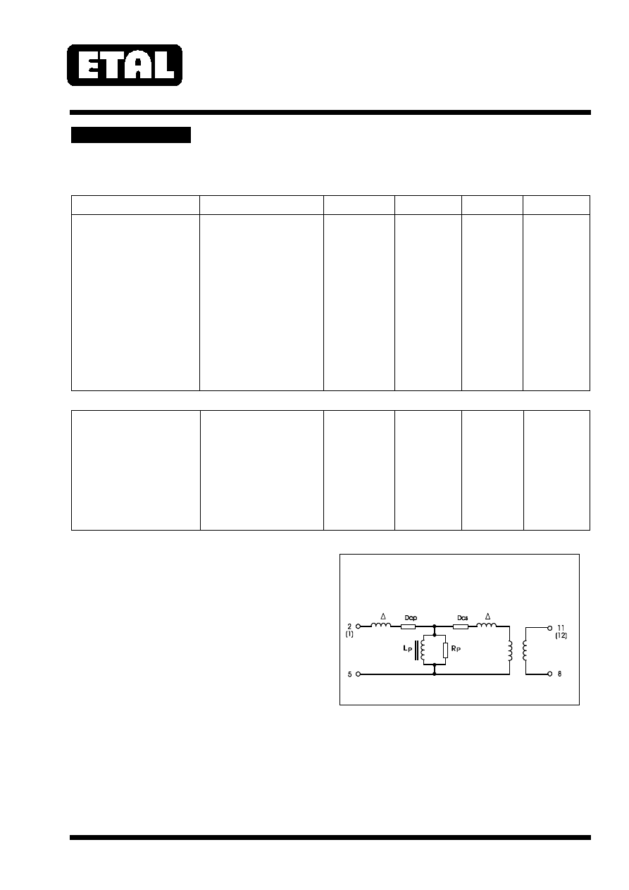
Lumped equivalent circuit parameters as Fig. 1
DC resistance
(3)
R
DCP
R
DCS
Primary resistance
Secondary resistance
-
-
160
190
-
-
Ω
Ω
Leakage inductance,
∆
L
-
0.8
-
mH
Shunt inductance, Lp
(4)
200Hz -43dBm
-
12
-
H
Shunt loss, Rp
200Hz -43dBm
-
40
-
k
Ω
Notes:
1. Third harmonic typically exceeds other
harmonics by 10dB.
2. Components are 100% tested at 1.75kVrms
minimum.
3. Caution: do not pass DC through windings.
Telephone line current must be diverted using
semiconductor line hold circuit or equivalent.
4. At signal levels greater than –20dBm, Lp will
increase and Rp will decrease slightly but the
effect is usually favourable to the return loss
characteristic.
Equivalent Circuit
Fig. 1
IDEAL
1:1
½ L
½ L
R
R
P369X
ETALDOC 715/2
Page 3 of 4
September 2002
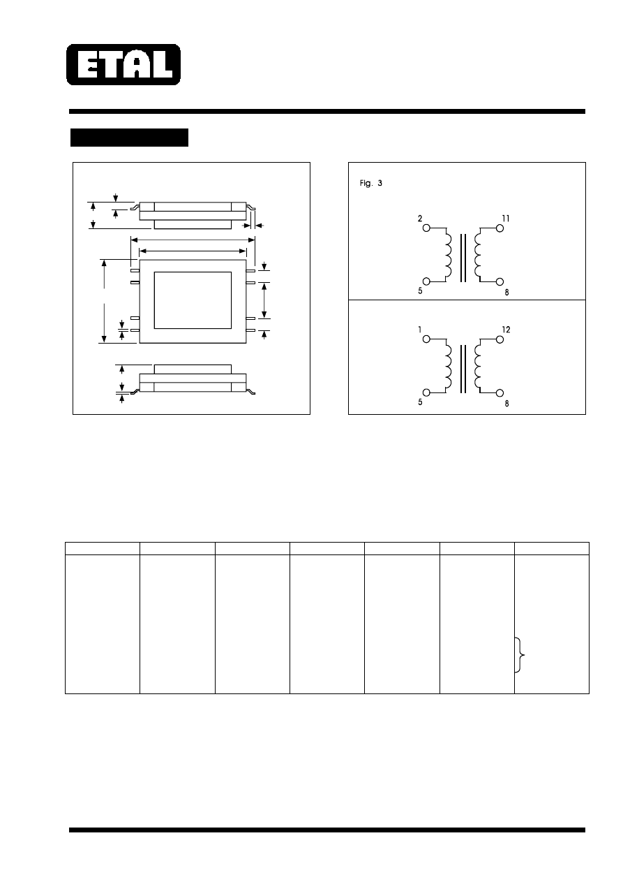
CONSTRUCTION
Dimensions shown are in millimetres (inches).
Windings may be used interchangeably as primary or secondary.
Recommended PCB pad sizes 1.2 x 0.8mm (0.047" x 0.031") on centres dimension C-0.7mm (C-0.028")
Note: to prolong solderability, circuit terminals are shipped with a very fine solderable surface protection. This
surface coating assists soldering and is completely depleted during the soldering process. However, this
coating is not removed by other means of attachment e.g. conductive epoxy. Parts suitable for use with
conductive epoxy can be supplied on special order.
Identity
Type
A max
B*
C ref
D*
Other
P3690
T.B.
4.37 (0.172")
1.27 (0.050")
19.8 (0.78")
--
--
P3691
T.B.
4.37 (0.172")
2.44 (0.096")
21.8 (0.86")
--
--
P3695
SMD
5.08 (0.200")
--
19.8 (0.78")
0.13 (0.005")
--
P3696
SMD
4.50 (0.177")
--
19.8 (0.78")
0.13 (0.005")
--
P3697
T.B.
4.27 (0.168")
2.44 (0.096")
20.6 (0.81")
--
P3698
T.B.
4.37 (0.172")
2.44 (0.096")
20.1 (0.79")
--
4 Pin
versions. Only
pins 1, 5, 8,
12 present
*Tolerance on dimensions B and D ±0.076mm (±0.003").
For other custom configurations please contact ETAL.
For international applications, see associated family P370X.
Connections
SECONDARY
PRIMARY
SECONDARY
PRIMARY
P3690, P3691, P3695, P3696
P3697, P3698
B
D
0.75(0.03“)
A
A
THROUGH BOARD (T.B.) TYPE
C Ref
16.8Max
(0.66Max)
2.03 TYP
(0.08)
2.03 TYP
(0.08)
6.1 TYP
(0.24)
0.4
(0.16)
13.7Max
(0.54Max)
1
2
5
6
12
11
8
7
Dimensions
Fig. 2
SMD TYPE
P369X
ETALDOC 715/2
Page 4 of 4
September 2002
MATCHING RECOMMENDATION
The following implementation assumes a low impedance balanced TX drive and a relatively high impedance
RX input, as is commonly available, though use with other TX/RX arrangements is straightforward. Note that
there need be no changes to components on the line side, or in the hybrid, if a complex reference impedance
is to be matched, thus assisting country configuration.
Frequency Response : ±0.1dB 30Hz – 10kHz
Return Loss: 25dB 200Hz – 4kHz
Transhybrid Loss: 18dB 200Hz – 4kHz
ABSOLUTE MAXIMUM RATINGS
COPYRIGHT
(Ratings of components independent of circuit).
Short term isolation voltage (1s)
DC current
Storage temperature
Reflow/terminal temperature.
1.25kVrms,
1.77kVDC
100
µ
A
-40
O
C to
+155
O
C
250
O
C
ETAL, P369X, P3690, P3691, P3695, P3696,
P3697 and P3698 are Trade Marks of Electronic
Techniques (Anglia) Limited.
The Trade Mark ETAL is registered at the UK
Trade Marks Registry.
© 1999 Electronic Techniques (Anglia) Limited.
Reproduction prohibited.
T R A N S F O R M I N G T H E F U T U R E
Profec Technologies Ltd., 10 Betts Avenue, Martlesham Heath, Ipswich, IP5 3RH, England
Telephone: +44 (0) 1473 611422
Fax: +44 (0) 1473 611919
Websites: www.etal.ltd.uk
www.profec.com
Email:
info@etal.ltd.uk
sales@profec.com
600
Ω
Fig. 4
LINE
600
330
1.8k
10k
RXA
TXA2
TXA1
µ
22 F
Patents Pending
FM 25326
ISO 9001