ETALDOC 776/4
Page 1 of 5
January 2004
PRODUCT DATA SHEET
LOW DISTORTION
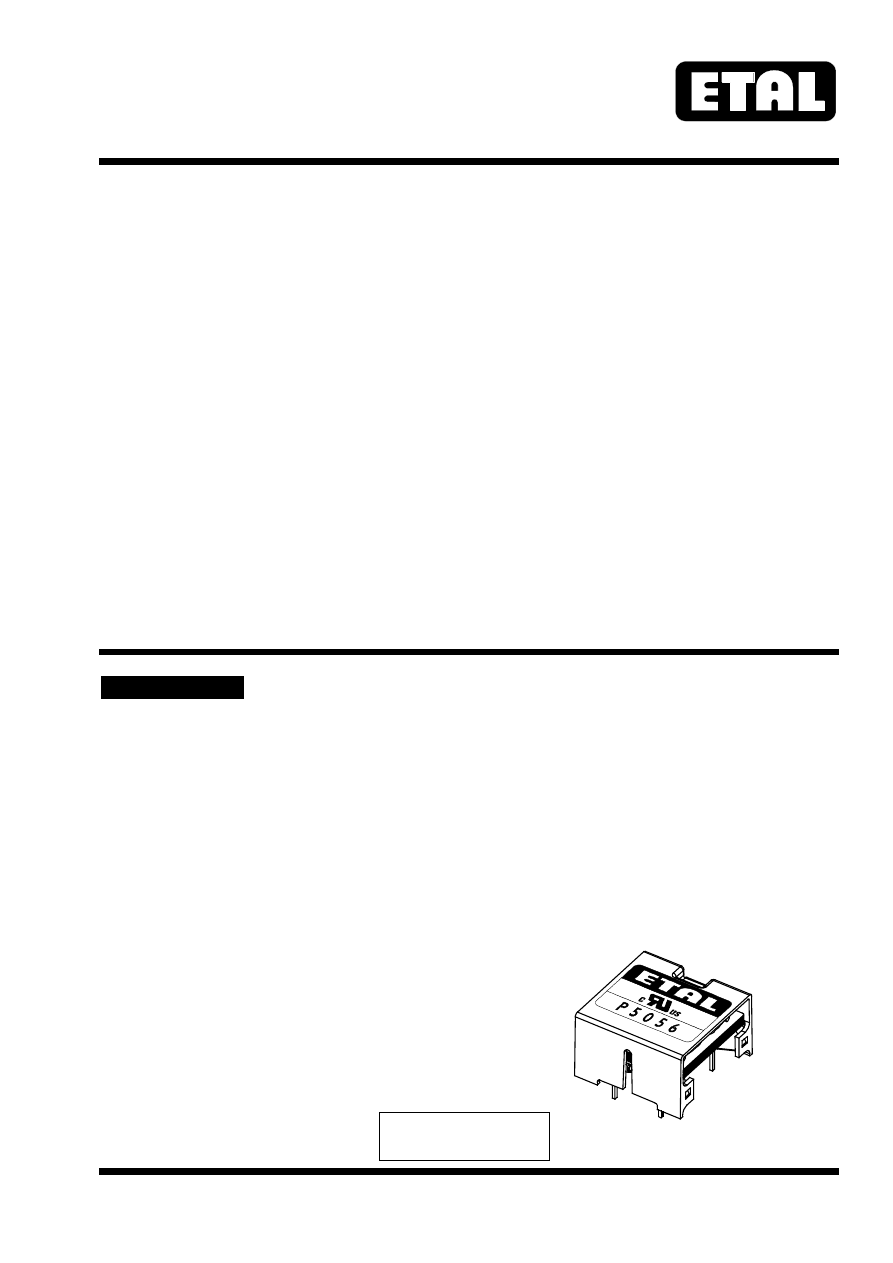
P5056
LINE MATCHING TRANSFORMER
Features
Applications
∗
Lead-free (Pb-free)
∗
V.90 and V.92 Modems
∗
Low Distortion
∗
V.34 Modems
∗
11mm (0.43”) Seated Height
∗
Fax Machines
∗
Industry Standard Pinout
∗
Instrumentation
∗
IEC 60950 and UL 60950 Certified
∗
Set Top Box/Web browsing
∗
UL Recognized Component
∗
Internet Feature Phones
∗
Extended Frequency Response
∗
Flat TX and RX Responses
∗
Simple Matching
∗
Low Insertion Loss
∗
High Thermal Stability
DESCRIPTION
P5056 is intended for low cost V.90 and V.92
(56kbps) modems and other high-speed
applications where low distortion at moderate
power levels and very low voiceband frequencies is
required.
P5056 uses patented design and construction
methods to achieve excellent signal performance
and safety isolation to international standards. The
part is completely lead-free and suitable for
lead-free and conventional processing.
P5056 has exceptionally flat frequency response
from 30Hz to 10kHz, a 3dB bandwidth of 60kHz
and requires only the very simplest of matching to
achieve good return loss and transhybrid loss
across the voiceband, with very low levels of signal
distortion at signal frequencies as low as 150Hz.
P5056 also exhibits stable characteristics over its
full operating temperature range to maximize
data throughput under varying environmental
conditions without the need for modem
retraining.
P5056 is certified to IEC 60950 and UL 60950.
P5056 is a UL Recognized Component and is
supported by an IEC CB certificate.
Patented