FEATURES:
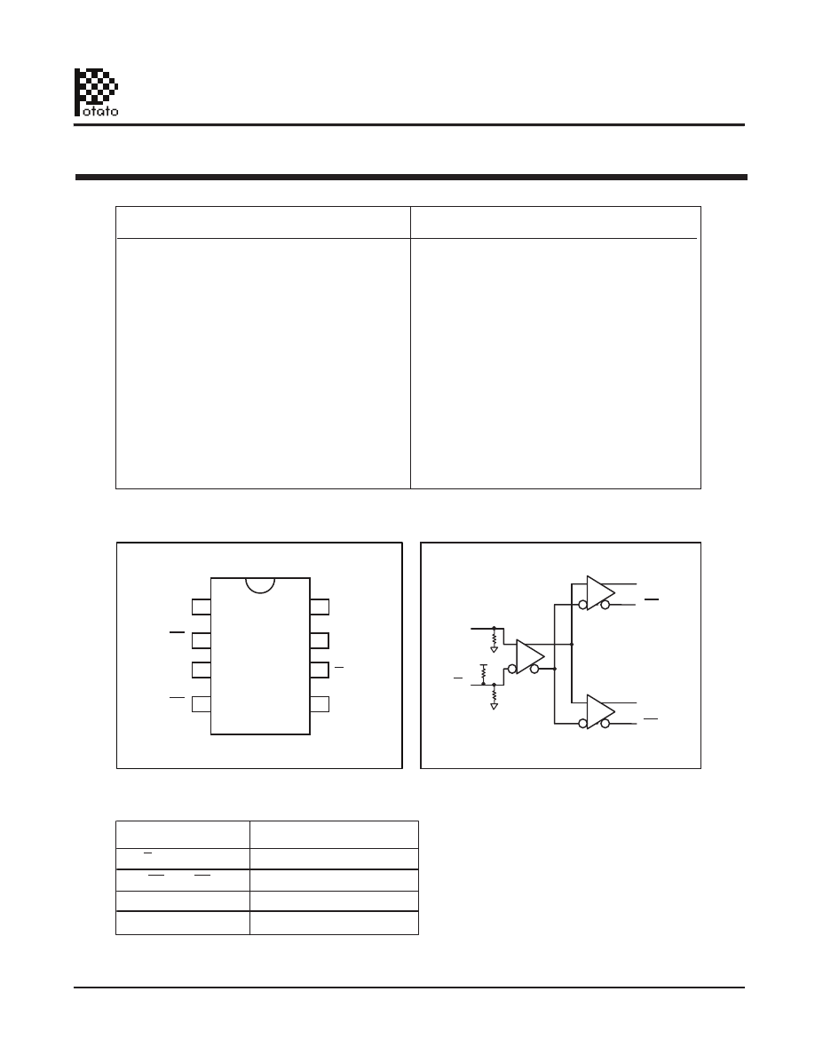
Pin Configuration
Logic Block Diagram
Pin Description
DESCRIPTION:
Potato Semiconductor’s PO100HSTL11A is
designed for world top performance using
submicron CMOS technology to achieve 1.24GHz
HSTL output frequency with less than 2.0ns
propagation delay.
The
PO100HSTL11A
is a low-skew, 1-to-2
differential fanout buffer targeted to meet the
requirements of high-performance clock and data
distribution applications. The device has a fully
differential internal architecture that is optimized
to achieve low signal skews at operating frequen-
cies of up to 1.24GHz .
Vcc
D
D
D
GND
Q0
Q0
Q0
Q1
Q1
Q1
1
2
3
4
8
7
6
5
PIN
D, D
Q0, Q0, Q1, Q1
HSTL Outputs
FUNCTION
LVDS LVPECL HSTL Inputs
V
CC
GND
Ground Supply
Positive Supply
Q0
Q1
D
• Patented Technology
• Two HSTL differential outputs
• One pair of LVDS/LVPECL/HSTL/ differential
or single-ended inputs
• Operating frequency up to 1.24GHz with 2pf load
• Operating frequency up to 900MHz with 5pf load
• Operating frequency up to 400MHz with 15pf load
• Very low output pin to pin skew < 40ps
• Propagation delay < 2.0ns max with 15pf load
• 2.3V to 3.6V power supply
• Industrial temperature range: –40°C to 85°C
• Available in 8-pin SOIC package
• Available in 8-pin TSSOP package
2.3V - 3.6V 1 to 2 Differential Clock/Data Fanout Buffer
1.24GHz Noise Cancellation TTL/CMOS Potato Chip
1
01/01/10
Potato Semiconductor Corporation
PO100HSTL11A
www.potatosemi.com
PO100HSTL11A-html.html
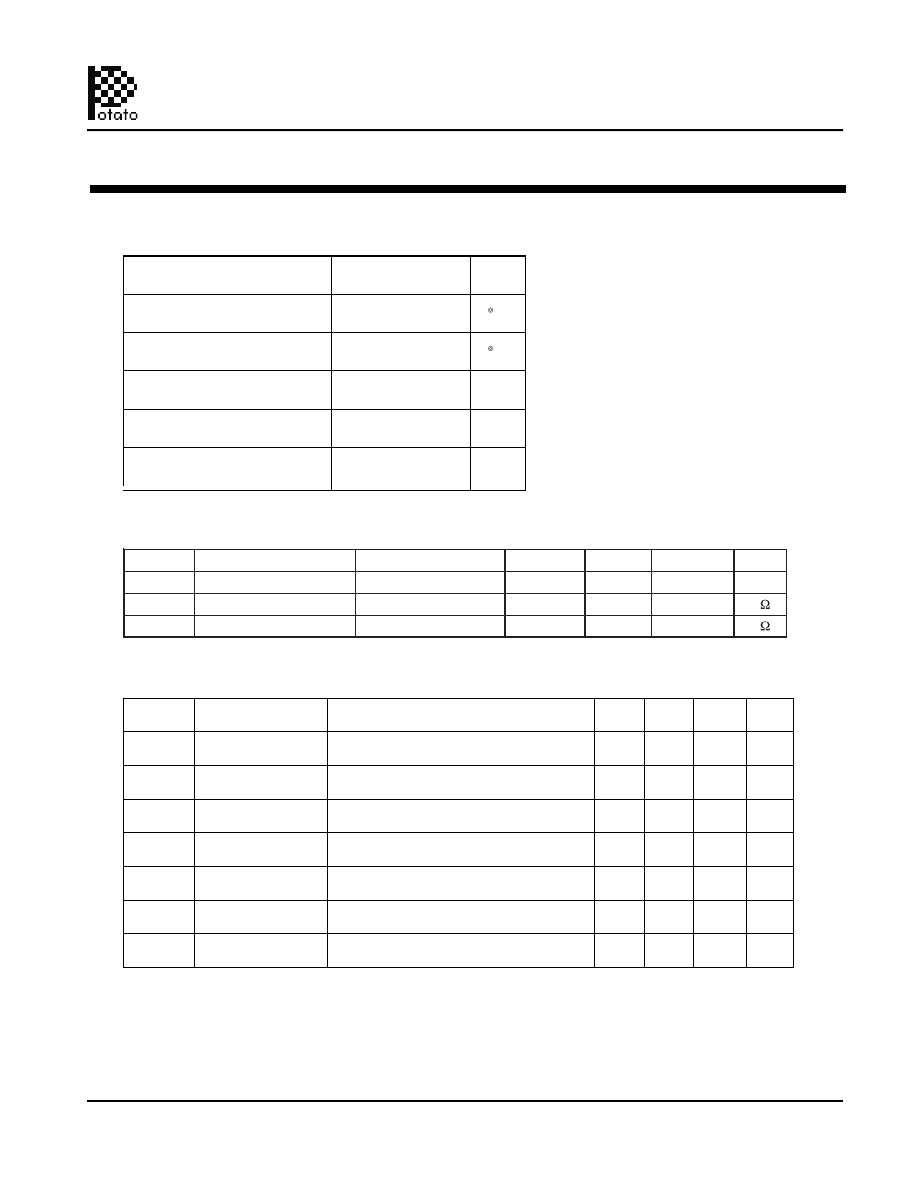
Maximum Ratings
DC Electrical Characteristics
Symbol
Description
Test Conditions
Min
Typ
Max
Unit
V
OH
Output High voltage
Vcc=3V Vin=V
IH
or V
IL
, I
OH
= -12mA
2.4
3
-
V
V
OL
Output Low voltage
Vcc=3V Vin=V
IH
or V
IL
, I
OH
=12mA
-
0.3
0.5
V
V
IH
Input High voltage
Guaranteed Logic HIGH Level (Input Pin)
2
-
Vcc
V
V
IL
Input Low voltage
Guaranteed Logic LOW Level (Input Pin)
-0.5
-
0.8
V
I
IH
Input High current
Vcc = 3.6V and Vin = Vcc
-
-
1
uA
I
IL
Input Low current
Vcc = 3.6V and Vin = 0V
-
-
-1
uA
V
IK
Clamp diode voltage
Vcc = Min. And
I
IN
= -18mA
-
-0.7
-1.2
V
Notes:
1. For conditions shown as Max. or Min., use appropriate value specified under Electrical Characteristics for the applicable device type.
2.
Typical values are at Vcc = 3.3V, 25
°
C ambient.
3.
This parameter is guaranteed but not tested.
4.
Not more than one output should be shorted at one time. Duration of the test should not exceed one second.
5.
VoH = Vcc – 0.6V at rated current
Description
Max
Unit
Storage Temperature
-65 to 150
°
C
Operation Temperature
-40 to 85
°
C
Operation Voltage
-0.5 to +4.6
V
Input Voltage
-0.5 to Vcc
V
Output Voltage
-0.5 to Vcc+0.5
V
Note:
stresses greater than listed under
Maximum
Ratings
may
cause
permanent damage to the device. This
is a stress rating only and functional
operation of the device at these or any
other conditions above those indicated
in the operational sections of this
specification is not implied. Exposure
to absolute maximum rating conditions
for extended periods may affect
reliability specification is not implied.
Pin Characteristics
l
o
b
m
y
S
r
e
t
e
m
a
r
a
s
P
n
o
it
i
d
n
o
C
t
s
e
m
T
u
m
i
n
i
M
l
a
c
i
p
y
T
m
u
m
i
x
a
M
s
ti
n
U
C
N
I
e
c
n
a
ti
c
a
p
a
C
t
u
p
n
I
F
4
p
R
P
U
L
L
U
P
r
o
t
si
s
e
R
p
u
ll
u
P
t
u
p
n
I
88
88
K
K
R
N
W
O
D
L
L
U
P
r
o
t
si
s
e
R
n
w
o
d
ll
u
P
t
u
p
n
I
2.3V - 3.6V 1 to 2 Differential Clock/Data Fanout Buffer
1.24GHz Noise Cancellation TTL/CMOS Potato Chip
2
01/01/10
Potato Semiconductor Corporation
PO100HSTL11A
www.potatosemi.com
PO100HSTL11A-html.html
Power Supply Characteristics
Symbol
Description
Test Conditions (1)
Min
Typ
Max
Unit
Icc
Q
Quiescent Power Supply Current
Vcc=Max, Vin=Vcc or GND
-
0.1
30
uA
Notes:
1. For conditions shown as Max. or Min., use appropriate value specified under Electrical Characteristics for the applicable device type.
2. Typical values are at Vcc = 3.3V, 25
•
C ambient.
3. This parameter is guaranteed but not tested.
4. Not more than one output should be shorted at one time. Duration of the test should not exceed one second.
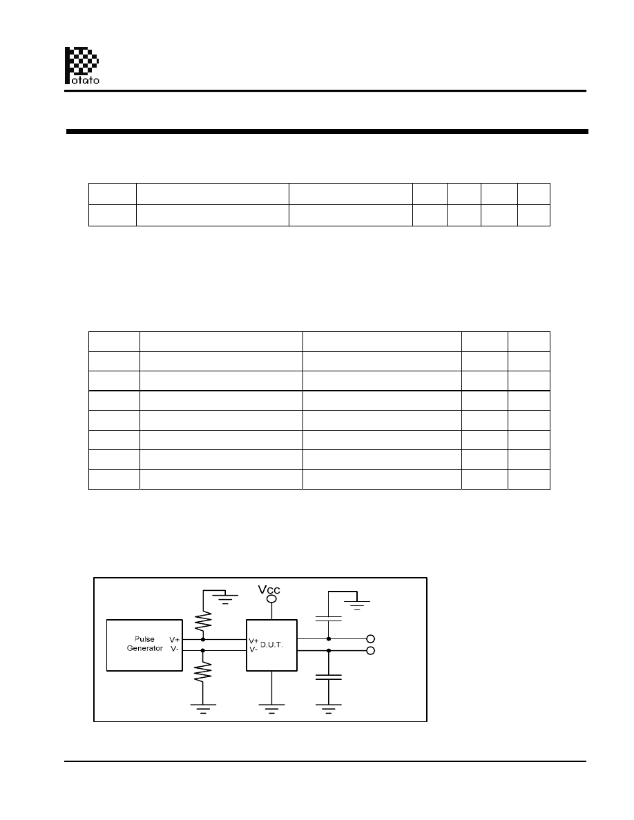
Switching Characteristics
t
i
n
U
x
a
M
)
1
(
s
n
o
i
t
i
d
n
o
C
t
s
e
T
n
o
i
t
p
i
r
c
s
e
D
l
o
b
m
y
S
t
PD
Propagation Delay D to Output pair
CL = 15pF
2.0
ns
tr/tf
Rise/Fall Time
0.8V – 2.0V
0.8
ns
tsk(o)
Output Pin to Pin Skew (Same Package)
ps
ps
tsk(pp)
Output Skew (Different Package)
fmax
F
p
5
1
=
L
C
y
c
n
e
u
q
e
r
F
t
u
p
n
I
250
MHz
fmax
F
p
5
=
L
C
y
c
n
e
u
q
e
r
F
t
u
p
n
I
300
MHz
fmax
F
p
2
=
L
C
y
c
n
e
u
q
e
r
F
t
u
p
n
I
400
MHz
Notes:
1. See test circuits and waveforms.
2. tpLH, tpHL, tsk(p), and tsk(o) are production tested. All other parameters guaranteed but not production tested.
3. Airflow of 1m/s is recommended for frequencies above 133MHz
CL = 15pF, 125MHz
CL = 15pF, 125MHz
40
250
400
900
1240
Test Circuit
50Ohm
50Ohm
15pF
to
2pF
15pF
to
2pF
2.3V - 3.6V 1 to 2 Differential Clock/Data Fanout Buffer
1.24GHz Noise Cancellation TTL/CMOS Potato Chip
3
01/01/10
Potato Semiconductor Corporation
PO100HSTL11A
www.potatosemi.com
PO100HSTL11A-html.html
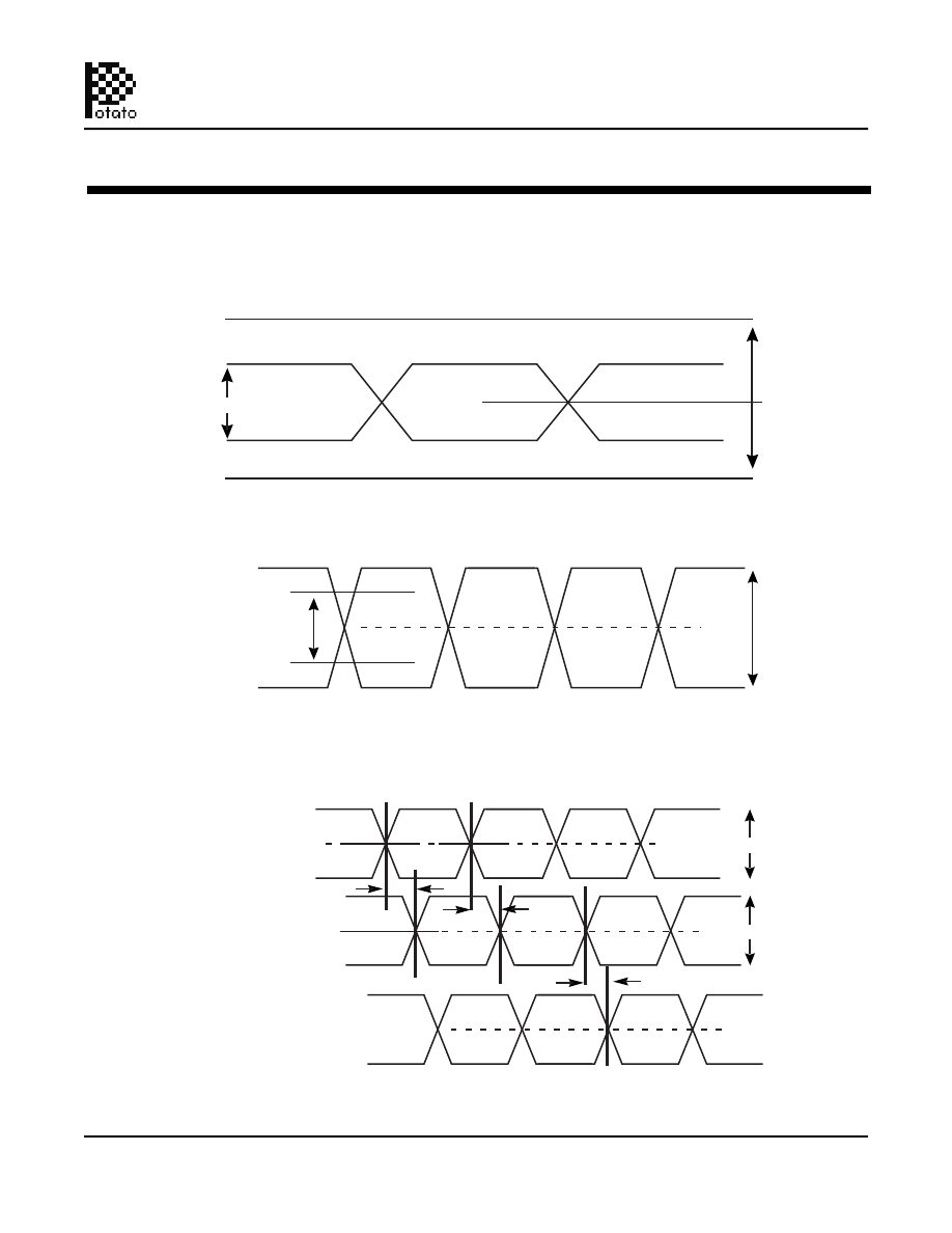
Test Waveforms
VPP RANGE
0V-VCC
FIGURE 1. LVDS/ PECL/ ECL/ HSTL /DIFFERENTIAL INPUT WAVEFORM DEFINITIONS
FIGURE 2. HSTL/HSTL OUTPUT
FIGURE 3. Propogation Delay, Output pulse skew, and output-to-output skew
for D to output pair
VPP
TPHL
TPLH
TPD
INPUT
CLOCK
OUTPUT
CLOCK
ANOTHER
OUTPUT
CLOCK
VO
tSK(O)
VCC= 3.3V
VEE=0.0V
VIH
VIL
VPP
VCC
VEE
VO
tr,tf,
20-80%
2.3V - 3.6V 1 to 2 Differential Clock/Data Fanout Buffer
1.24GHz Noise Cancellation TTL/CMOS Potato Chip
4
01/01/10
Potato Semiconductor Corporation
PO100HSTL11A
www.potatosemi.com
PO100HSTL11A-html.html
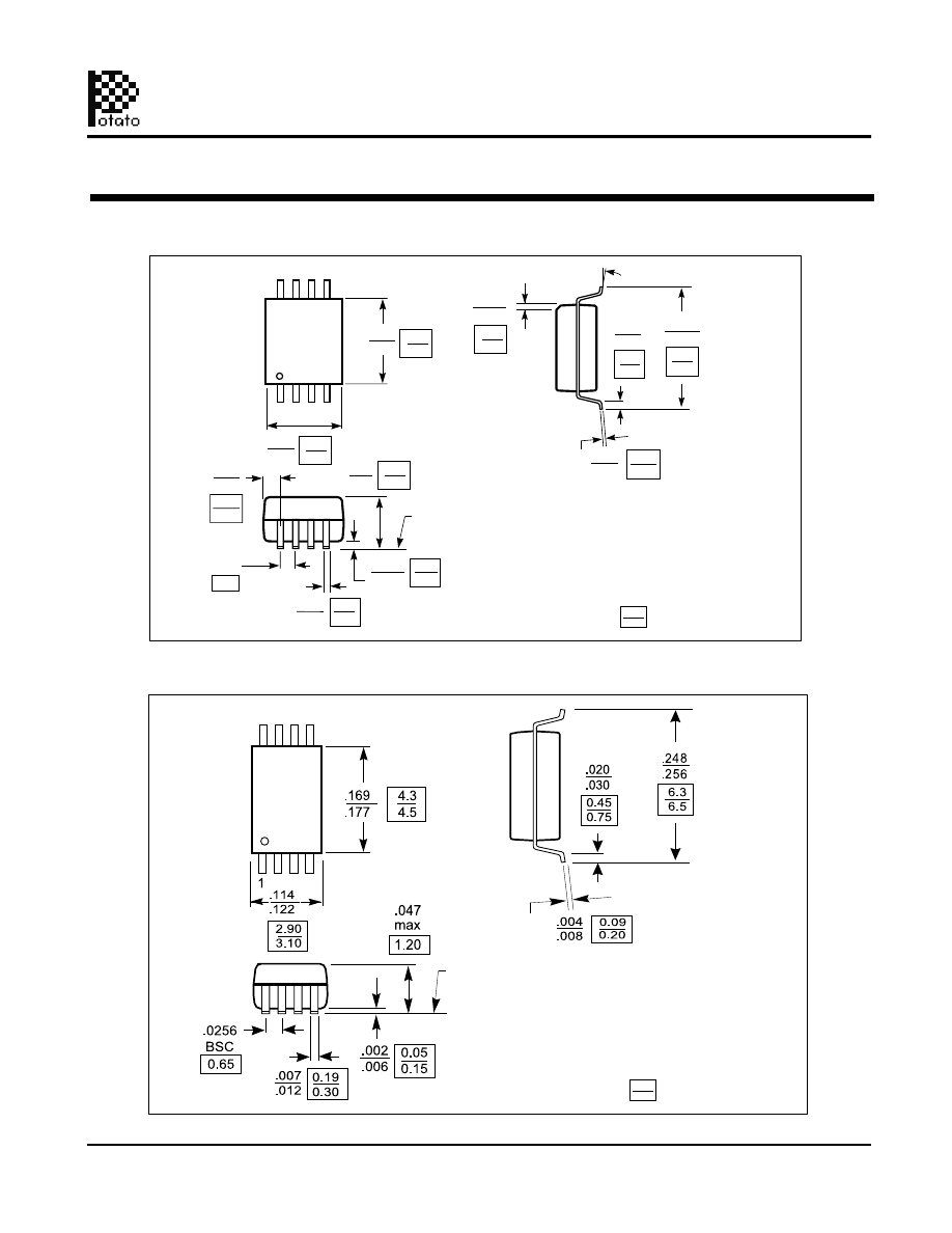
Packaging Mechanical Drawing: 8 pin SOIC
X.XX
X.XX
DENOTES DIMENSIONS
IN MILLIMETERS
.0040
.0098
SEATING PLANE
.013
.020
.050
BSC
1
8
.149
.157
3.78
3.99
.189
.196
4.80
5.00
1.27
.016
.026
1.35
1.75
0.406
0.660
0.330
0.508
0.10
0.25
.053
.068
REF
.016
.0075
.0098
.0099
.0196
0-8˚
.050
.2284
.2440
5.80
6.20
0.40
1.27
0.19
0.25
0.25
0.50
x 45˚
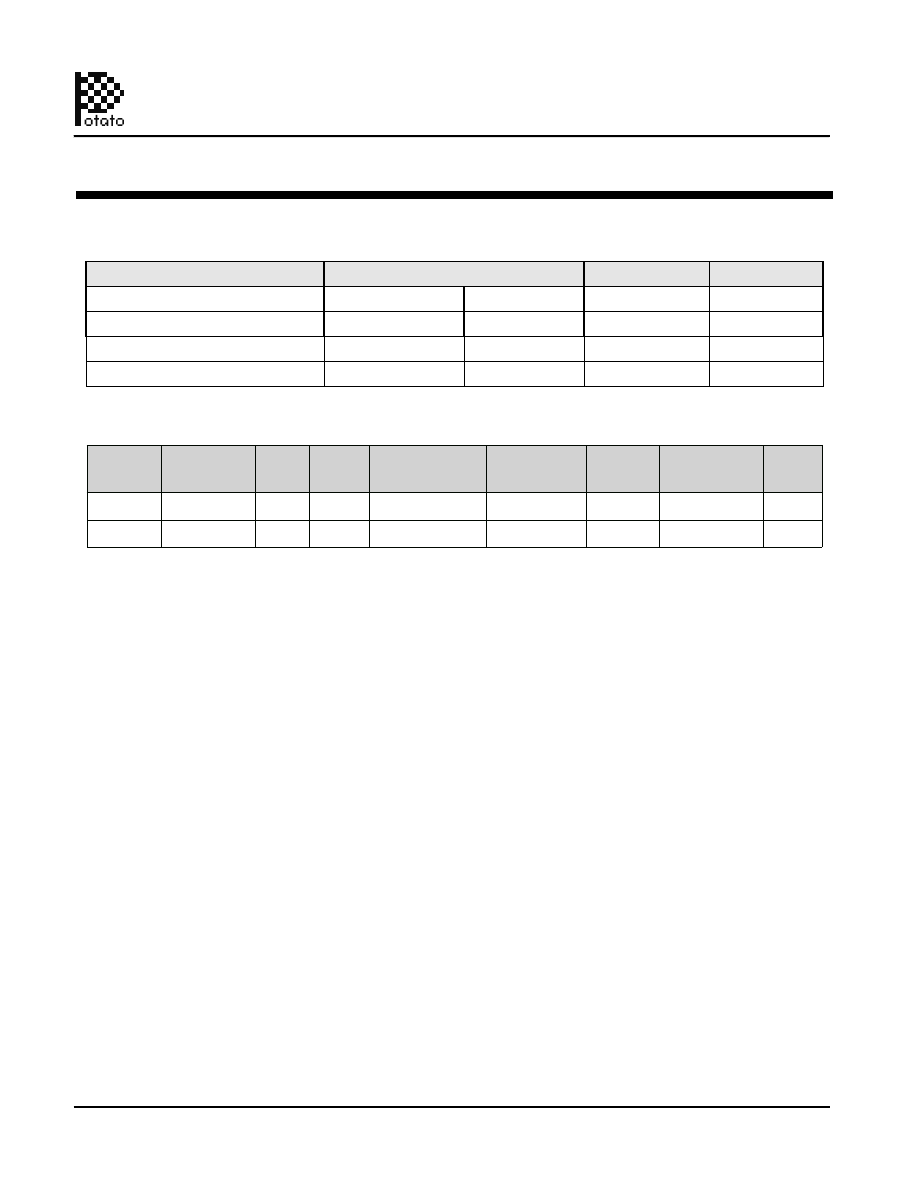
Packaging Mechanical Drawing: 8 pin TSSOP
X.XX
X.XX
DENOTES DIMENSIONS
IN MILLIMETERS
SEATING PLANE
8
2.3V - 3.6V 1 to 2 Differential Clock/Data Fanout Buffer
1.24GHz Noise Cancellation TTL/CMOS Potato Chip
5
01/01/10
Potato Semiconductor Corporation
PO100HSTL11A
www.potatosemi.com
PO100HSTL11A-html.html
2.3V - 3.6V 1 to 2 Differential Clock/Data Fanout Buffer
Top-Marking
IC Ordering Information
Ordering Code
Package
8pin 150mil SOIC
Pb-free & Green
PO100HSTL11ASU for Tube
PO100HSTL11AS
PO100HSTL11AS
PO100HSTL11ASR for Tape & Reel
-40
°
C to 85
°
C
-40
°
C to 85
°
C
TA
PO100HSTL11ATU for Tube
PO100HSTL11ATR for Tape & Reel
PO100HSTL11AT
PO100HSTL11AT
-40°C to 85°C
-40°C to 85°C
1.24GHz Noise Cancellation TTL/CMOS Potato Chip
6
01/01/10
Potato Semiconductor Corporation
PO100HSTL11A
www.potatosemi.com
8pin 150mil SOIC
Pb-free & Green
8pin 150mil TSSOP Pb-free & Green
Pb-free & Green
8pin 150mil TSSOP
IC Package Information
PACKAGE
S
12
8
39 (12”)
3000
64 (20”)
97
8pin 150mil SOIC
CODE
PACKAGE
TYPE
TAPE
WIDTH
TAPE TRAILER
TUBE
TAPE & REEL
LENGTH
TAPE
PITCH
QTY
LENGTH
TAPE LEADER
PER TAPE
QTY
PER
PIN 1 LOCATION
(mm)
(mm)
T
12
8
39 (12”)
3000
64 (20”)
158
8pin 173mil TSSOP
Top Left Corner
Top Left Corner