FEATURES:
DESCRIPTION:
• Patented technology
• High signal -3db passing bandwidth at 1.2GHz
• Near-Zero propagation delay
• VCC = 1.65V to 3.6V
• Ultra-Low Quiescent Power: 0.1µA typical
• Ideally suited for low power applications
• Industrial operating temperature: -40
°C to +85°C
• Available in 16pin 173mil wide TSSOP package
Potato Semiconductor’s PO3B3257A is
designed for world top performance using
submicron CMOS technology to achieve GHz
high bandwidth.
The PO3B3257A is a 4-channel, 2:1 Multiplexer /
Demultiplexer with 3-state outputs. The switch
introduces no additional ground bounce noise or
propagation delay.
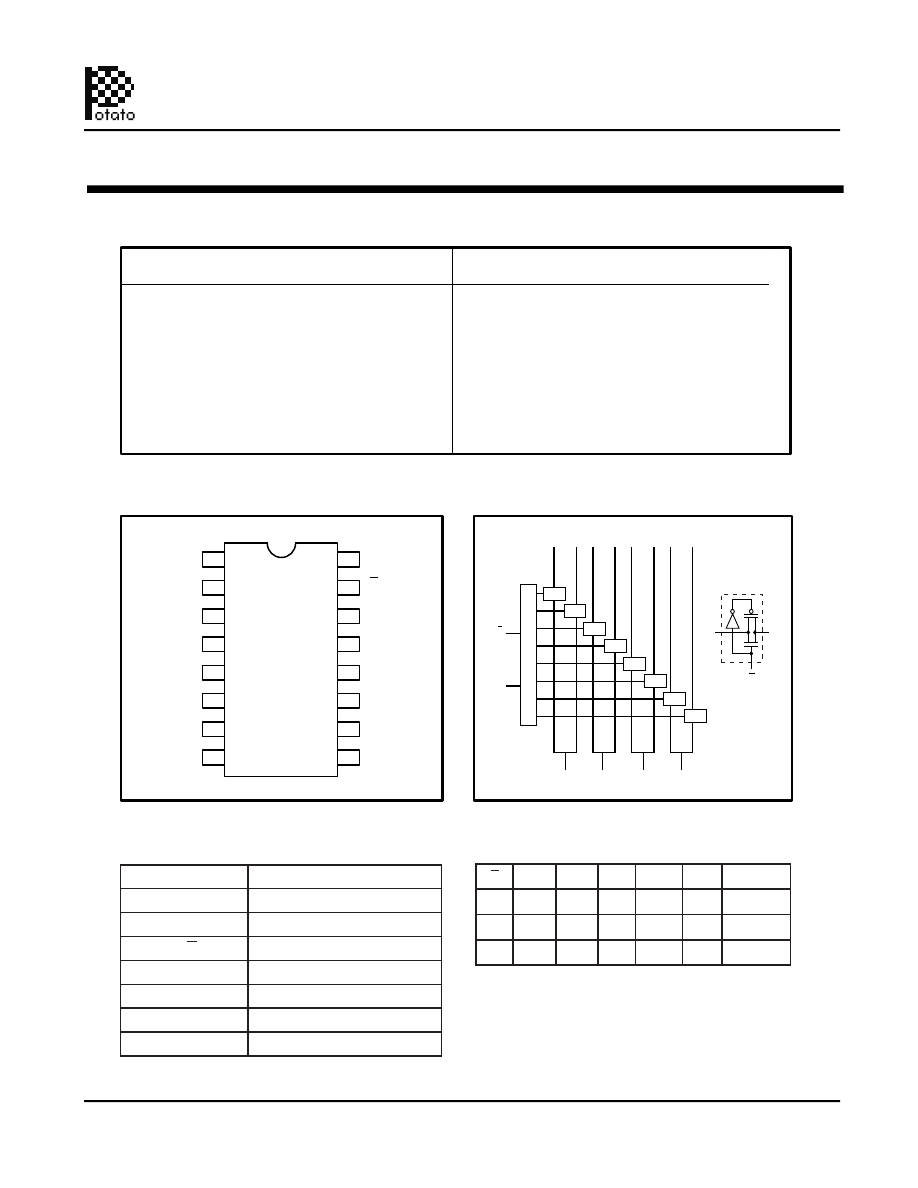
Pin Configuration
Block Diagram
Pin Description
1
2
3
4
5
16
6
15
7
14
8
13
12
11
10
9
S
Y
A
GND
V
CC
Y
C
Y
B
Truth Table
E
I
A
0
I
A
0
I
A
1
I
A
1
I
B
0
I
B
0
I
B
1
I
B
1
I
C
0
I
C
0
I
C
1
I
C
1
I
D
0
I
D
0
I
D
1
I
D
1
S
Y
A
E
Y
B
Y
C
Y
D
Y
D
I
Y
E
SW
SW
SW
SW
SW
SW
SW
SW
SW
Pin Name
Description
I
A
N
-
I
D
N
Data Inputs
S
Select Inputs
E
Enable
Y
A
-Y
D
Data Outputs
GND
Ground
V
CC
Power
NC
No Connect
E
S
Y
A
Y
B
Y
C
Y
D
Function
H
X
Hi-Z Hi-Z
Hi-Z
Hi-Z Disable
L
L
I
A
0
I
B
0
I
C
0
I
D
0
S = 0
L
H
I
A
1
I
B
1
I
C
1
I
D
1
S = 1
Quad 2:1 Mux/DeMux
High Bandwidth Potato Chip
1
01/01/10
Potato Semiconductor Corporation
PO3B3257A
www.potatosemi.com