background image

FEATURES:

DESCRIPTION:

• Patented technology
• High signal -3db passing bandwidth at 1GHz
• Near-Zero propagation delay
• VCC = 1.65V to 3.6V
• Ultra-Low Quiescent Power: 0.1µA typical
• Ideally suited for low power applications
• Industrial operating temperature: -40

°C to +85°C

• Available in 40pin 5mm x 5mm QFN package

Potato Semiconductor’s PO3B402A is
designed for world top performance using
submicron CMOS technology to achieve GHz
high bandwidth.

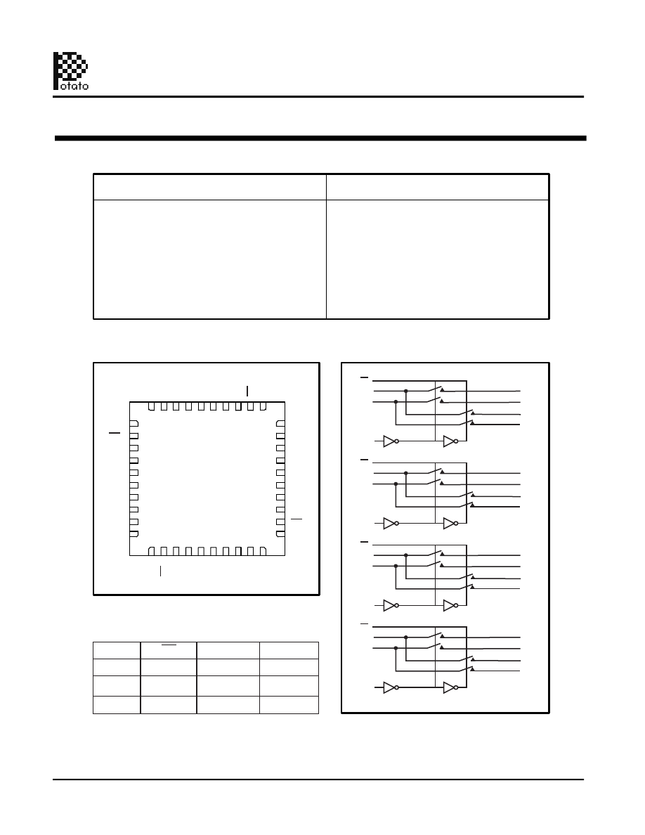
The PO3B402A is a 4-Port 2-channel, 2:1 
Multiplexer /Demultiplexer with  3-state outputs. 
The switch introduces no additional ground 
bounce  noise or propagation delay.

Pin Configuration

Block Diagram

Truth Table

GND

V

DD

SEL1

SEL1

Y1-

Y1+

Y1-

Y1+

OE1

OE1

M1+

M1-

M1+

M1-

D1+

D1-

D1+

D1-

SEL2

Y2-

Y2+

OE2

M2+

M2-

D2+

D2-

SEL3

Y3-

Y3+

OE3

M3+

M3-

D3+

D3-

SEL4

Y4-

Y4+

OE4

M4+

M4-

D4+

D4-

10

11

20

21

30

31

40

1

GND

V

DD

SEL2

Y

2

-

Y2+

OE2

M2+

M2-

D2+

D2-

GND

V

DD

SEL3

Y3-

Y3+

OE3

M3+

M3-

D3+

D3-

GND

V

DD

SEL4

Y

4

-

Y4+

OE4

M4+

M4-

D4+

D4-

OEn

Yn+

Yn-

X

H

Hi-Z

Hi-Z

L

L

Mn+

Mn-

H

L

Dn+

Dn-

SELn

4-Port 2-Channel, 2:1 Mux/DeMux Switch

High Bandwidth Potato Chip 

1

01/01/10

Potato Semiconductor Corporation

PO3B402A

www.potatosemi.com

PO3B402A-html.html
background image

Storage Temperature ................................................ –65°C to +150°C
Ambient Temperature with Power Applied ............... –40°C to +85°C
Supply Voltage to Ground Potential ........................... –0.5V to +4.6V
DC Input Voltage ........................................................ –0.5V to +Vcc
DC Output Current................................................................... 120mA
Power Dissipation ....................................................................... 0.5W

Maximum Ratings

(Above which the useful life may be impaired. For user guidelines, not tested.)

DC Electrical Characteristics, 3.3V Supply 

(Over the Operating Range, T

A

 = –40°C to +85°C, V

CC

 = 3.3V ±10%)

Parameters

Description

Test Conditions

Min. Typ.

Max. Units

V

IH

Input HIGH Voltage

Guaranteed Logic HIGH Level

2.0

V

V

IL

Input LOW Voltage

Guaranteed Logic LOW Level

0.8

I

IH

Input HIGH Current

V

CC

 = Max., V

IN

 = V

CC

±1

A

I

IL

Input LOW Current

V

CC

 = Max., V

IN

 = GND

±1

I

OZH

High Impedance Output Current 0 Y, In V

CC

±1

R

ON

Switch On-Resistance

V

CC

= Min., V

IN

= 0.0V,

I

ON

 = -48 mA or -64mA

14

18

V

CC

= Min., V

IN

= V

CC

, I

ON

 = -15 mA

16

20

DC Electrical Characteristics, 2.5V Supply 

(Over  Operating Range, T

A

 = –40°C to +85°C, V

CC

= 2.5V ± 10%)

Parameters

Description

Test Conditions

Min.

Typ.

Max.

Units

V

IH

Input HIGH Voltage

Guaranteed Logic HIGH Level

1.8

V

CC

 + 0.3

V

V

IL

Inout LOW Voltage

Guaranteed Logic LOW Level

–0.3

0.8

I

IH

Input HIGH Current

V

CC

 = Max., V

IN

 = V

CC

±1

A

I

IL

Input LOW Current

V

CC

 = Max., V

IN

= GND

±1

I

OZH

High Impedance Current

0 Y, In  V

CC

±1

R

ON

Switch On Resistance

V

CC

 = Min., V

IN

 = 0.0V,

I

ON

 = –48mA

18

22

V

CC

 = Min., V

IN

 = Vcc, 

I

ON

 = -15mA

18

22

Note:

Stresses greater than those listed under
MAXIMUM RATINGS may cause permanent
damage to the device. This is a stress rating
only and functional operation of the device at
these or any other conditions above those
indicated in the operational sections of this

specification

is not implied. Exposure to

absolute maximum rating conditions for
extended periods may affect reliability.

4-Port 2-Channel, 2:1 Mux/DeMux Switch

High Bandwidth Potato Chip 

2

01/01/10

Potato Semiconductor Corporation

PO3B402A

www.potatosemi.com

PO3B402A-html.html
background image

Power Supply Characteristics

Symbol

Description

Test Conditions (1)

Min

Typ

Max

Unit

Icc

Quiescent Power Supply Current

Vcc=Max, Vin=Vcc or GND

-

0.1

3

uA

Notes:

1. For conditions shown as Max. or Min., use appropriate value specified under Electrical Characteristics for the applicable device type.
2. Typical values are at Vcc = 3.3V, 25

°

C ambient.

3. This parameter is guaranteed but not tested.
4. Not more than one output should be shorted at one time. Duration of the test should not exceed one second.
5. VoH = Vcc – 0.6V at rated current

Capacitance

(T

A

 = 25°C f = 1 MHz)

Switching Characteristics over 3.3V Operating Range

Parameters

Description

Conditions

Units

Max.

t

PLH

t

PHL

See Test Diagram

0.3

ns

t

PZH

t

PZL

See Test Diagram

2.0

t

PHZ

t

PLZ

3.0

Dynamic Electrical Characteristics Over the Operating Range 

(T

A

 = -40º to +85º, V

CC

 = 3.3V ± 10%)

Parameter

Description

Test Condition

Typ.

Units

X

TALK

Crosstalk

R

L

 = 100

-60

dB

O

IRR

Off-Isolation

R

L

 = 100

-60

BW

-3dB Bandwidth

R

L

 = 100

1

GHz

Parameters

Description

Test Conditions

Typ.

Units

C

IN

Input Capacitance

V

IN

 = 0V

3.0

pF

C

OFF

Port I Capacitance, Switch OFF

5.0

C

ON

Switch Capacitance, Switch ON

10.0

Propogation Delay

Bus Enable Time

Bus Disable Time

4-Port 2-Channel, 2:1 Mux/DeMux Switch

High Bandwidth Potato Chip 

3

01/01/10

Potato Semiconductor Corporation

PO3B402A

www.potatosemi.com

PO3B402A-html.html
background image

Switching Characteristics over 2.5V Operating Range

Parameters

Description

Conditions

Units

Max.

t

PLH

t

PHL

See Test Diagram

0.3

ns

t

PZH

t

PZL

See Test Diagram

2.0

t

PHZ

t

PLZ

3.0

Test Circuit for Electrical Characteristics

R

T

10pF

C

L

V

CC

V

IN

V

OUT

200-ohm

200-ohm

6.0V

Pulse

Generator

D.U.T

Switch Positions

Test

Switch

t

PLZ

, t

PZL

6.0V

t

PHZ

, t

PZH

GND

Prop Delay 

Open

Switching Waveforms

tPLZ

1.25V

1.25V

2.5V

VOH

0V

VOL

VDD/2

VDD/2

tPHZ

tPZL

tPZH

Output

Output

VOL +0.3V

VOH –0.3V

VOL
VOH

SEL

Input

t

PLH

2.5V

2.5V

2.5V

2.5V

t

PHL

3.5V

1.5V

Output

V

OH

V

OL

Voltage Waveforms Propagation Delay Times

Voltage Waveforms Enable and Disable Times

Propogation Delay

Bus Enable Time

Bus Disable Time

4-Port 2-Channel, 2:1 Mux/DeMux Switch

High Bandwidth Potato Chip 

4

01/01/10

Potato Semiconductor Corporation

PO3B402A

www.potatosemi.com

PO3B402A-html.html
background image

Packaging Mechanical Drawing: 40 pin QFN

20

11

10

21

1

30

31

40

40

31

1

11

10

20

4-Port 2-Channel, 2:1 Mux/DeMux Switch

High Bandwidth Potato Chip 

5

01/01/10

Potato Semiconductor Corporation

PO3B402A

www.potatosemi.com

IC Ordering Information

Top-Marking

Ordering Code

Package

PO3B402AQFR for Tape & Reel

PO3B402AQF

-40

°

C to 85

°

C

TA

40-pin QFN

IC Package Information

PACKAGE

QF

16

12

Top Left Corner

26 (12”)

3000

43 (20”)

N/A

CODE

PACKAGE

TYPE

TAPE

WIDTH

TAPE TRAILER

TUBE

TAPE & REEL

LENGTH

TAPE

PITCH

QTY

LENGTH

TAPE LEADER

PER TAPE

QTY
PER

PIN 1 LOCATION

(mm)

(mm)

Pb-free & Green

40-pin QFN