background image

FEATURES:

DESCRIPTION:

. Patented technology
. Operating frequency up to 500MHz with 2pf load
. Operating frequency up to 400MHz with 5pf load
. Operating frequency up to 250MHz with 50pf load
. Very low output pin to pin skew < 100ps
. Very low pulse skew < 300ps
. VCC = 1.65V to 3.6V
. Propagation delay < 2.5ns max with 50pf load
. Low input capacitance: 3pf typical
. 4x1:4 fanout
. Available in 28pin 50mil PLCC package

Potato Semiconductor’s PO49FCT1816G is
designed for world top performance using
submicron

CMOS

technology

to

achieve

500MHz TTL output frequency with less than
100ps output pin to pin skew.

PO49FCT1816G is a 1.65V to 3.3V CMOS 1
input to 4 outputs Buffered driver in 4 groups to
achieve 500MHz output frequency. Typical
applications are clock and signal distribution.
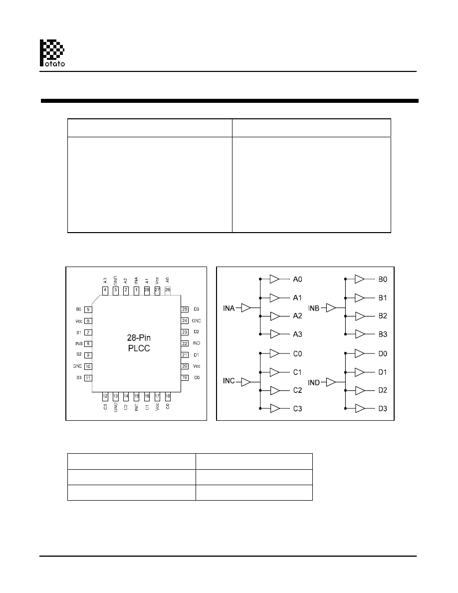
Pin Configuration

Logic Block Diagram

Pin Description

Pin Name

Description

INA, INB, INC, IND

Inputs

A[0-3], B[0-3], C[0-3], D[0-3]

Outputs

4X1:4 CMOS Clock Buffered Driver

1

01/01/10

Potato Semiconductor Corporation

PO49FCT1816

www.potatosemi.com

500MHz TTL/CMOS Potato Chip

PO49FCT1816G-html.html
background image

Maximum Ratings

DC Electrical Characteristics

Symbol

Description

Test Conditions

Min

Typ

Max

Unit

V

OH

Output High voltage

Vcc=3V Vin=V

IH

or V

IL

, I

OH

= -24mA

2.46

-

V

V

OL

Output Low voltage

Vcc=3V Vin=V

IH

or V

IL

, I

OH

=24mA

-

0.44

V

V

IH

Input High voltage

Guaranteed Logic HIGH Level (Input Pin)

2

-

Vcc

V

V

IL

Input Low voltage

Guaranteed Logic LOW Level (Input Pin)

-0.5

-

0.8

V

I

IH

Input High current

Vcc = 3.6V and Vin = 3.6V

-

-

1

uA

I

IL

Input Low current

Vcc = 3.6V and Vin = 0V

-

-

-1

uA

V

IK

Clamp diode voltage

Vcc = Min. And

I

IN

= -18mA

-

-0.7

-1.2

V

Notes:

1. For conditions shown as Max. or Min., use appropriate value specified under Electrical Characteristics for the applicable device type.
2.

Typical values are at Vcc = 3.3V, 25

°

C ambient.

3.

This parameter is guaranteed but not tested.

4.

Not more than one output should be shorted at one time. Duration of the test should not exceed one second.

5.

VoH = Vcc – 0.6V at rated current

Description

Max

Unit

Storage Temperature

-65 to 150

°

C

Operation Temperature

-40 to 85 

°

C

Operation Voltage

-0.5 to +4.6 

V

Input Voltage

-0.5 to Vcc+0.5

V

Output Voltage

-0.5 to Vcc+0.5

V

Note:

stresses greater than listed under
Maximum

Ratings

may

cause

permanent damage to the device. This
is a stress rating only and functional
operation of the device at these or any
other conditions above those indicated
in the operational sections of this
specification is not implied. Exposure
to absolute maximum rating conditions
for extended periods may affect
reliability specification is not implied.

4X1:4 CMOS Clock Buffered Driver

2

01/01/10

Potato Semiconductor Corporation

PO49FCT1816

www.potatosemi.com

500MHz TTL/CMOS Potato Chip

PO49FCT1816G-html.html
background image

Power Supply Characteristics

Symbol

Description

Test Conditions (1)

Min

Typ

Max

Unit

Icc

Q

Quiescent Power Supply Current

Vcc=Max, Vin=Vcc or GND

-

0.1

30

uA

Notes:

1. For conditions shown as Max. or Min., use appropriate value specified under Electrical Characteristics for the applicable device type.
2. Typical values are at Vcc = 3.3V, 25

°

C ambient.

3. This parameter is guaranteed but not tested.
4. Not more than one output should be shorted at one time. Duration of the test should not exceed one second.
5. VoH = Vcc – 0.6V at rated current

Capacitance

Parameters (1)

Description

Test Conditions

Typ

Max

Unit

Cin

Input Capacitance

Vin = 0V

3

4

pF

Cout

Output Capacitance

Vout = 0V

-

6

pF

Notes:

1 This parameter is determined by device characterization but not production tested.

Switching Characteristics

(

Vcc = 3.3V

±

0.3V, T

A

=85

°

C)

t

i

n

U

x

a

M

n

i

M

t

s

e

T

n

o

i

t

p

i

r

c

s

e

D

l

o

b

m

y

S

t

PLH

Propagation Delay A to Bn

CL = 50pF

2.5

ns

t

PHL

Propagation Delay A to Bn

CL = 50pF

2.5

ns

tr/tf

Rise/Fall Time Measured between 0.8V – 2.0V

CL = 50pf

2.0

ns

tsk(p)

Pulse Skew (Same Package)

CL = 50pF

0.3

ns

tsk(o)

Output Pin to Pin Skew (Same Bank)

CL = 50pF

0.1

ns

tsk(o)

Output Pin to Pin Skew (Same Package)

CL = 50pF

0.15

ns

tsk(pp)

Output Skew (Different Package)

CL = 50pF

0.4

ns

t

LOW/

t

HIGH

F

p

0

5

=

L

C

n

o

it

a

r

u

D

h

t

d

i

W

e

s

l

u

P

5

ns

t

DC

F

p

0

5

=

L

C

e

l

c

y

C

y

t

u

D

45

55

%

fmax

F

p

0

5

=

L

C

y

c

n

e

u

q

e

r

F

t

u

p

n

I

250

MHz

fmax

F

p

5

=

L

C

y

c

n

e

u

q

e

r

F

t

u

p

n

I

400

MHz

fmax

F

p

2

=

L

C

y

c

n

e

u

q

e

r

F

t

u

p

n

I

500

MHz

Notes:

1. See test circuits and waveforms.
2. tpLH, tpHL, tsk(p), and tsk(o) are production tested. All other parameters guaranteed but not production tested.
3. Airflow of 1m/s is recommended for frequencies above 133MHz

4X1:4 CMOS Clock Buffered Driver

3

01/01/10

Potato Semiconductor Corporation

PO49FCT1816

www.potatosemi.com

500MHz TTL/CMOS Potato Chip

PO49FCT1816G-html.html
background image

Test Waveforms

Test Circuit 1

50Ohm

4X1:4 CMOS Clock Buffered Driver

4

01/01/10

Potato Semiconductor Corporation

PO49FCT1816

www.potatosemi.com

500MHz TTL/CMOS Potato Chip

PO49FCT1816G-html.html
background image

Test Circuit 2

50Ohm

Packaging Mechanical Drawing: 28 pin PLCC

4X1:4 CMOS Clock Buffered Driver

5

01/01/10

Potato Semiconductor Corporation

PO49FCT1816

www.potatosemi.com

500MHz TTL/CMOS Potato Chip

PO49FCT1816G-html.html
background image

Ordering Information

Ordering Code

Package Code

Package Description

PO49FCT1816P

Pb-free & Green, 28-pin PLCC

4X1:4 CMOS Clock Buffered Driver

6

01/01/10

Potato Semiconductor Corporation

PO49FCT1816

www.potatosemi.com

500MHz TTL/CMOS Potato Chip