FEATURES:
DESCRIPTION:
. Operating frequency up to 500MHz with 2pf load
. Operating frequency up to 400MHz with 5pf load
. Operating frequency up to 230MHz with 15pf load
. Operating frequency up to 85MHz with 50pf load
. Very low output pin to pin skew < 250ps
. Very low pulse skew < 200ps
. VCC = 1.2V to 3.6V
. Propagation delay < 2.3ns max with 15pf load
. Low input capacitance: 3pf typical
. 1:7 fanout
. Available in 16pin 150mil wide QSOP package
. Available in 16pin 173mil wide TSSOP package
Potato Semiconductor’s PO49FCT32803G is
designed for world top performance using
submicron
CMOS
technology
to
achieve
500MHz output frequency with less than 250ps
output skew.
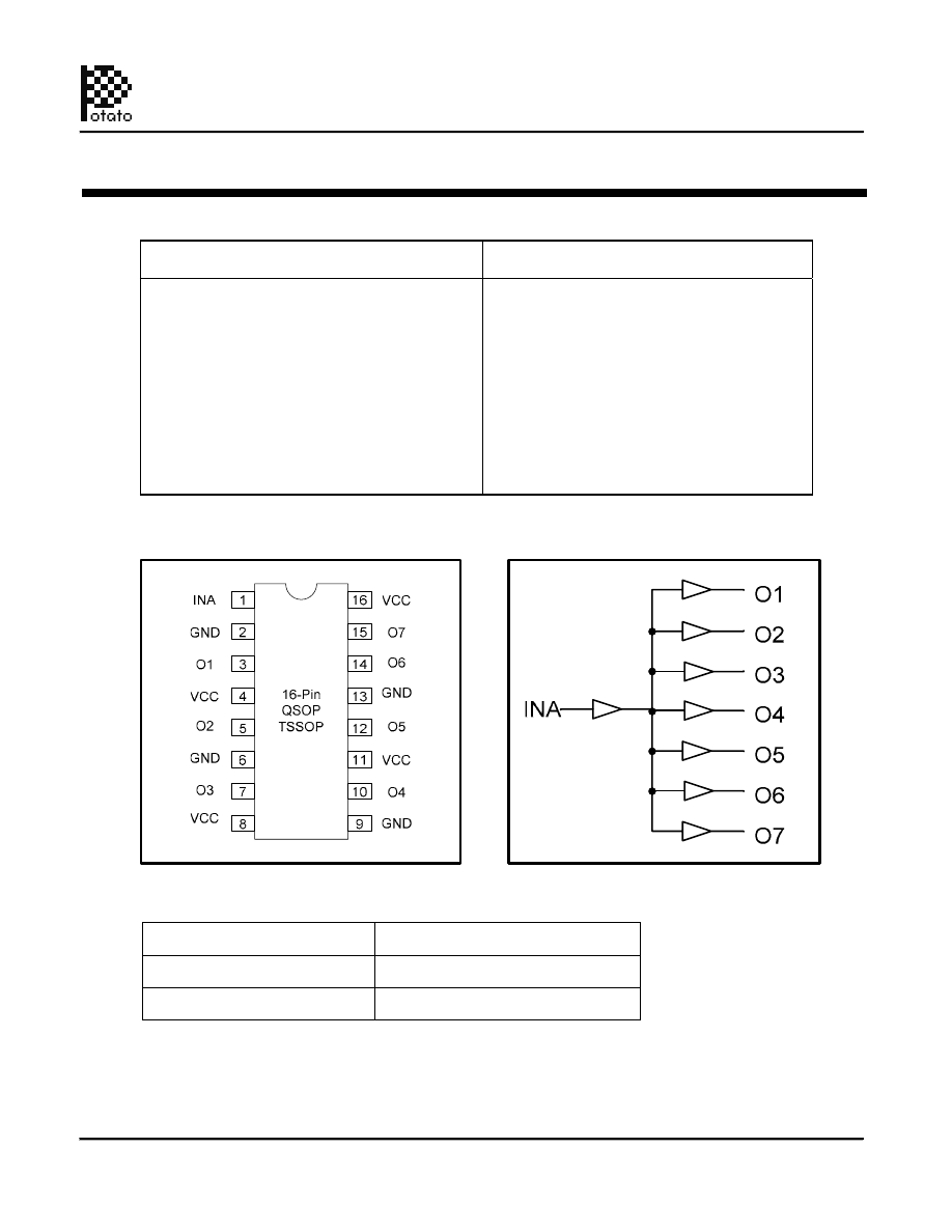
PO49FCT32803G is a 3.3V CMOS 1 input to 7
Output Buffered Driver with integrated series
damping resistors on all outputs to match 50 ohm
transmission line impedance. Typical applications
are clock and signal distribution.
Pin Configuration
Logic Block Diagram
Pin Description
Pin Name
Description
t
u
p
n
I
A
N
I
O1 to O7
Outputs
1.2V - 3.6V 1:7 CMOS Clock Buffered Driver
500MHz TTL/CMOS Potato Chip
1
01/01/10
Potato Semiconductor Corporation
PO49FCT32803G
www.potatosemi.com
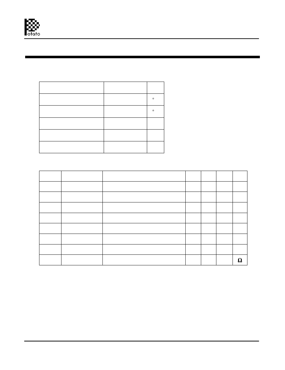
Maximum Ratings
DC Electrical Characteristics
Symbol
Description
Test Conditions
Min
Typ
Max
Unit
V
OH
Output High voltage
Vcc=3V Vin=V
IH
or V
IL
, I
OH
= -8mA
2.4
3
-
V
V
OL
Output Low voltage
Vcc=3V Vin=V
IH
or V
IL
, I
OH
=12mA
-
0.4
0.5
V
V
IH
Input High voltage
Guaranteed Logic HIGH Level (Input Pin)
2
-
Vcc
V
V
IL
Input Low voltage
Guaranteed Logic LOW Level (Input Pin)
-0.5
-
0.8
V
I
IH
Input High current
Vcc = 3.6V and Vin = 3.6V
-
-
1
uA
I
IL
Input Low current
Vcc = 3.6V and Vin = 0V
-
-
-1
uA
V
IK
Clamp diode voltage
Vcc = Min. And
I
IN
= -18mA
-
-0.7
-1.2
V
Rs
Series Resistor
22
Notes:
1. For conditions shown as Max. or Min., use appropriate value specified under Electrical Characteristics for the applicable device type.
2.
Typical values are at Vcc = 3.3V, 25
°
C ambient.
3.
This parameter is guaranteed but not tested.
4.
Not more than one output should be shorted at one time. Duration of the test should not exceed one second.
5.
VoH = Vcc – 0.6V at rated current
Description
Max
Unit
Storage Temperature
-65 to 150
°
C
Operation Temperature
-40 to 85
°
C
Operation Voltage
-0.5 to +4.6
V
Input Voltage
-0.5 to Vcc+0.5
V
Output Voltage
-0.5 to Vcc+0.5
V
Note:
stresses greater than listed under
Maximum
Ratings
may
cause
permanent damage to the device. This
is a stress rating only and functional
operation of the device at these or any
other conditions above those indicated
in the operational sections of this
specification is not implied. Exposure
to absolute maximum rating conditions
for extended periods may affect
reliability specification is not implied.
1.2V - 3.6V 1:7 CMOS Clock Buffered Driver
500MHz TTL/CMOS Potato Chip
2
01/01/10
Potato Semiconductor Corporation
PO49FCT32803G
www.potatosemi.com
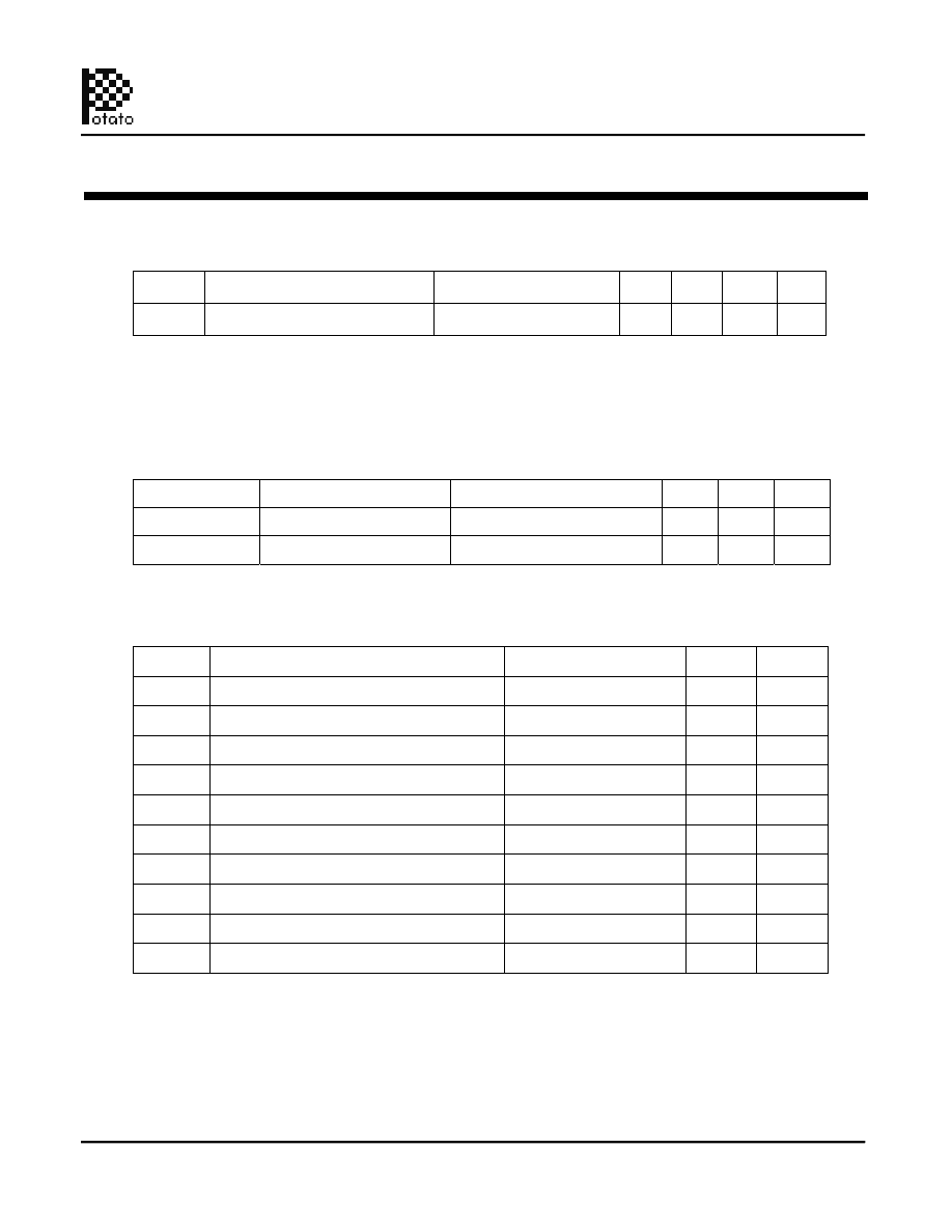
Power Supply Characteristics
Symbol
Description
Test Conditions (1)
Min
Typ
Max
Unit
Icc
Q
Quiescent Power Supply Current
Vcc=Max, Vin=Vcc or GND
-
0.1
30
uA
Notes:
1. For conditions shown as Max. or Min., use appropriate value specified under Electrical Characteristics for the applicable device type.
2. Typical values are at Vcc = 3.3V, 25
°
C ambient.
3. This parameter is guaranteed but not tested.
4. Not more than one output should be shorted at one time. Duration of the test should not exceed one second.
Capacitance
Parameters (1)
Description
Test Conditions
Typ
Max
Unit
Cin
Input Capacitance
Vin = 0V
3
4
pF
Cout
Output Capacitance
Vout = 0V
-
6
pF
Notes:
1 This parameter is determined by device characterization but not production tested.
Switching Characteristics
t
i
n
U
x
a
M
)
1
(
s
n
o
i
t
i
d
n
o
C
t
s
e
T
n
o
i
t
p
i
r
c
s
e
D
l
o
b
m
y
S
t
PLH
Propagation Delay A to Bn
CL = 15pF
2.3
ns
t
PHL
Propagation Delay A to Bn
CL = 15pF
2.3
ns
tr/tf
Rise/Fall Time
0.8V – 2.0V
1
ns
tsk(p)
F
p
5
1
=
L
C
)
e
g
a
k
c
a
P
e
m
a
S
(
w
e
k
S
e
s
l
u
P
0.2
ns
tsk(o)
Output Pin to Pin Skew (Same Package)
CL = 15pF
0.25 ns
tsk(pp)
F
p
5
1
=
L
C
)
e
g
a
k
c
a
P
t
n
e
r
e
f
f
i
D
(
w
e
k
S
t
u
p
t
u
O
0.4
ns
fmax
F
p
0
5
=
L
C
y
c
n
e
u
q
e
r
F
t
u
p
n
I
85
MHz
fmax
F
p
5
1
=
L
C
y
c
n
e
u
q
e
r
F
t
u
p
n
I
230
MHz
fmax
F
p
5
=
L
C
y
c
n
e
u
q
e
r
F
t
u
p
n
I
400
MHz
fmax
F
p
2
=
L
C
y
c
n
e
u
q
e
r
F
t
u
p
n
I
500
MHz
Notes:
1. See test circuits and waveforms.
2. tpLH, tpHL, tsk(p), and tsk(o) are production tested. All other parameters guaranteed but not production tested.
3. Airflow of 1m/s is recommended for frequencies above 133MHz
1.2V - 3.6V 1:7 CMOS Clock Buffered Driver
500MHz TTL/CMOS Potato Chip
3
01/01/10
Potato Semiconductor Corporation
PO49FCT32803G
www.potatosemi.com
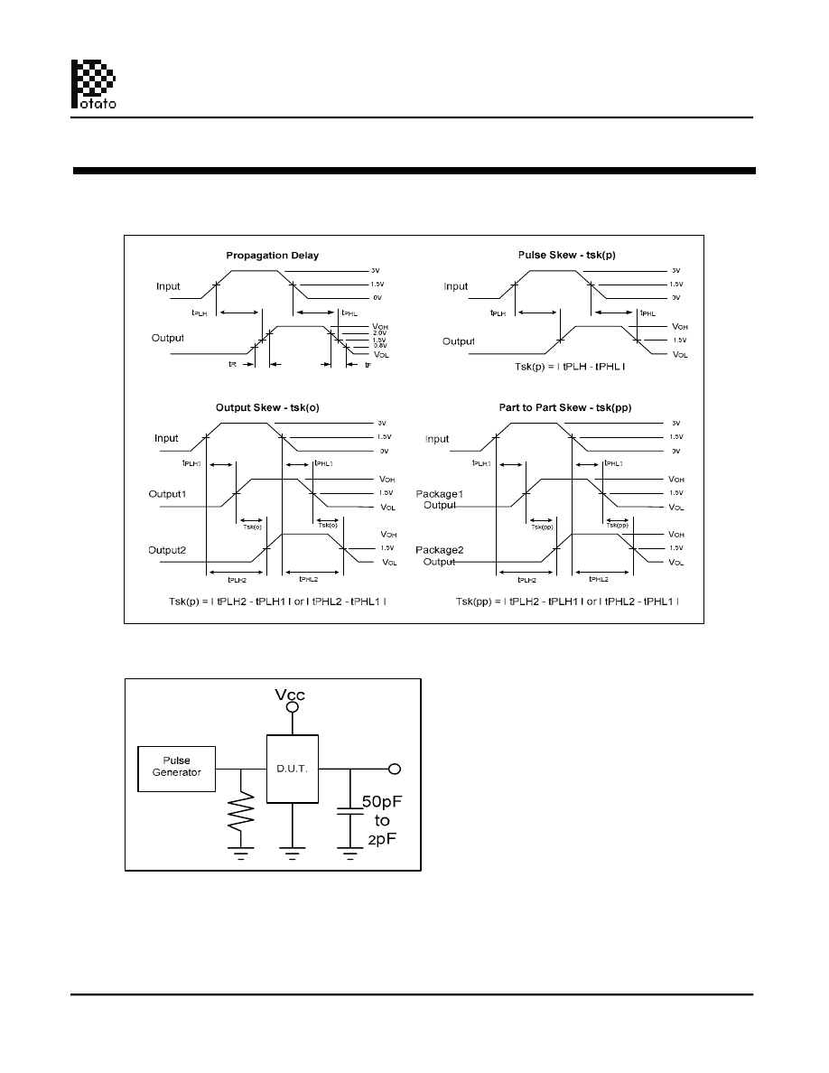
Test Waveforms
Test Circuit
50Ohm
1.2V - 3.6V 1:7 CMOS Clock Buffered Driver
500MHz TTL/CMOS Potato Chip
4
01/01/10
Potato Semiconductor Corporation
PO49FCT32803G
www.potatosemi.com
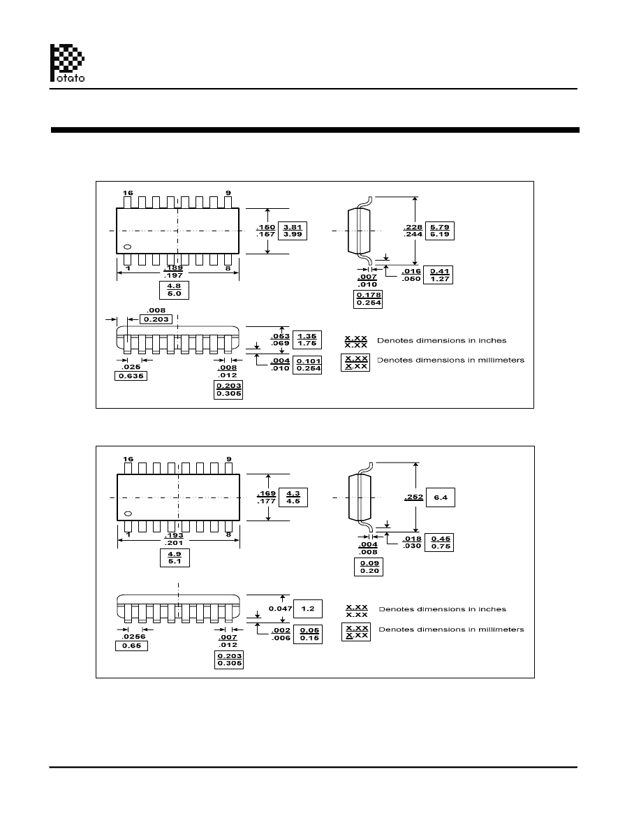
Packaging Mechanical Drawing: 16 pin QSOP
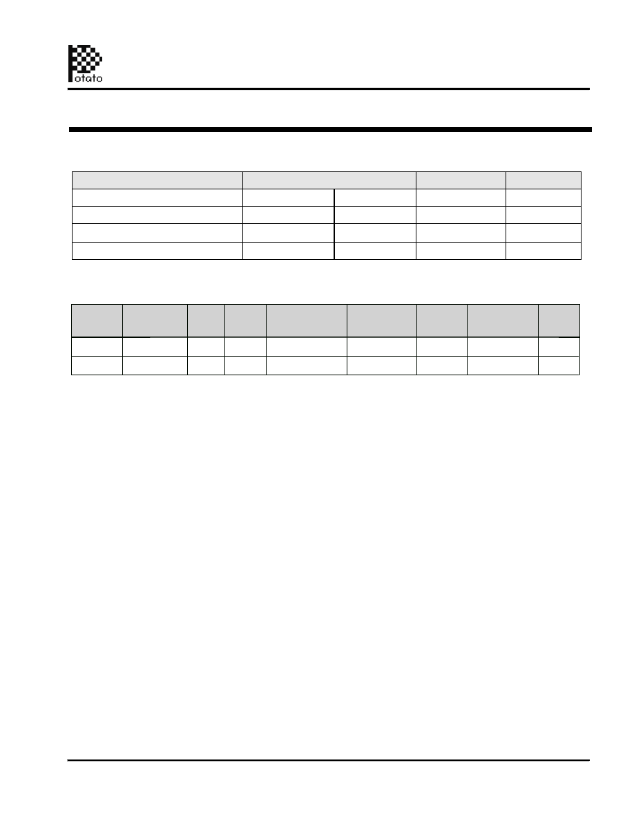
Packaging Mechanical Drawing: 16 pin TSSOP
1.2V - 3.6V 1:7 CMOS Clock Buffered Driver
500MHz TTL/CMOS Potato Chip
5
01/01/10
Potato Semiconductor Corporation
PO49FCT32803G
www.potatosemi.com
Top-Marking
Ordering Code
Package
PO49FCT32803GQU for Tube
PO49FCT32803GQR for Tape & Reel
PO49FCT32803GQ
PO49FCT32803GQ
-40
°
C to 85
°
C
-40
°
C to 85
°
C
PO49FCT32803GTU for Tube
PO49FCT32803GTR for Tape & Reel
PO49FCT32803GT
PO49FCT32803GT
-40
°
C to 85
°
C
-40
°
C to 85
°
C
TA
1.2V - 3.6V 1:7 CMOS Clock Buffered Driver
500MHz TTL/CMOS Potato Chip
6
01/01/10
Potato Semiconductor Corporation
PO49FCT32803G
www.potatosemi.com
IC Ordering Information
IC Package Information
PACKAGE
Q
12
8
39 (12”)
3000
64 (20”)
97
16pin 150mil QSOP
CODE
PACKAGE
TYPE
TAPE
WIDTH
TAPE TRAILER
TUBE
TAPE & REEL
LENGTH
TAPE
PITCH
QTY
LENGTH
TAPE LEADER
PER TAPE
QTY
PER
PIN 1 LOCATION
(mm)
(mm)
T
12
8
39 (12”)
3000
64 (20”)
96
16pin 173mil TSSOP
Top Left Corner
Pb-free & Green
Pb-free & Green
16-pin 150mil QSOP
Pb-free & Green
Pb-free & Green
16-pin 173mil TSSOP
16-pin 150mil QSOP
16-pin 173mil TSSOP
Top Left Corner