background image

FEATURES:

DESCRIPTION:

. Operating frequency up to 800MHz with 2pf load
. Operating frequency up to 600MHz with 5pf load
. Operating frequency up to 300MHz with 15pf load
. Operating frequency up to 100MHz with 50pf load
. Very low output pin to pin skew < 80ps
. Very low pulse skew < 300ps
. VCC = 1.2V to 3.6V
. Propagation delay < 2.4ns max with 15pf load
. Low input capacitance: 3pf typical
. Dual 1:5 fanout
. Available in 20pin 300mil wide SOIC package

. Available in 20pin 209mil wide SSOP package

. Available in 20pin 150mil wide QSOP package

Potato Semiconductor’s PO49FCT3805B is
designed for world top performance using
submicron

CMOS

technology

to

achieve

800MHz TTL output frequency with less than
80ps output pin to pin skew.

PO49FCT3805B is a 1.2V to  3.6V CMOS
Dual 1 input to 5 outputs Buffered driver to
achieve 800MHz output frequency.
Typical applications are clock and signal distribution.
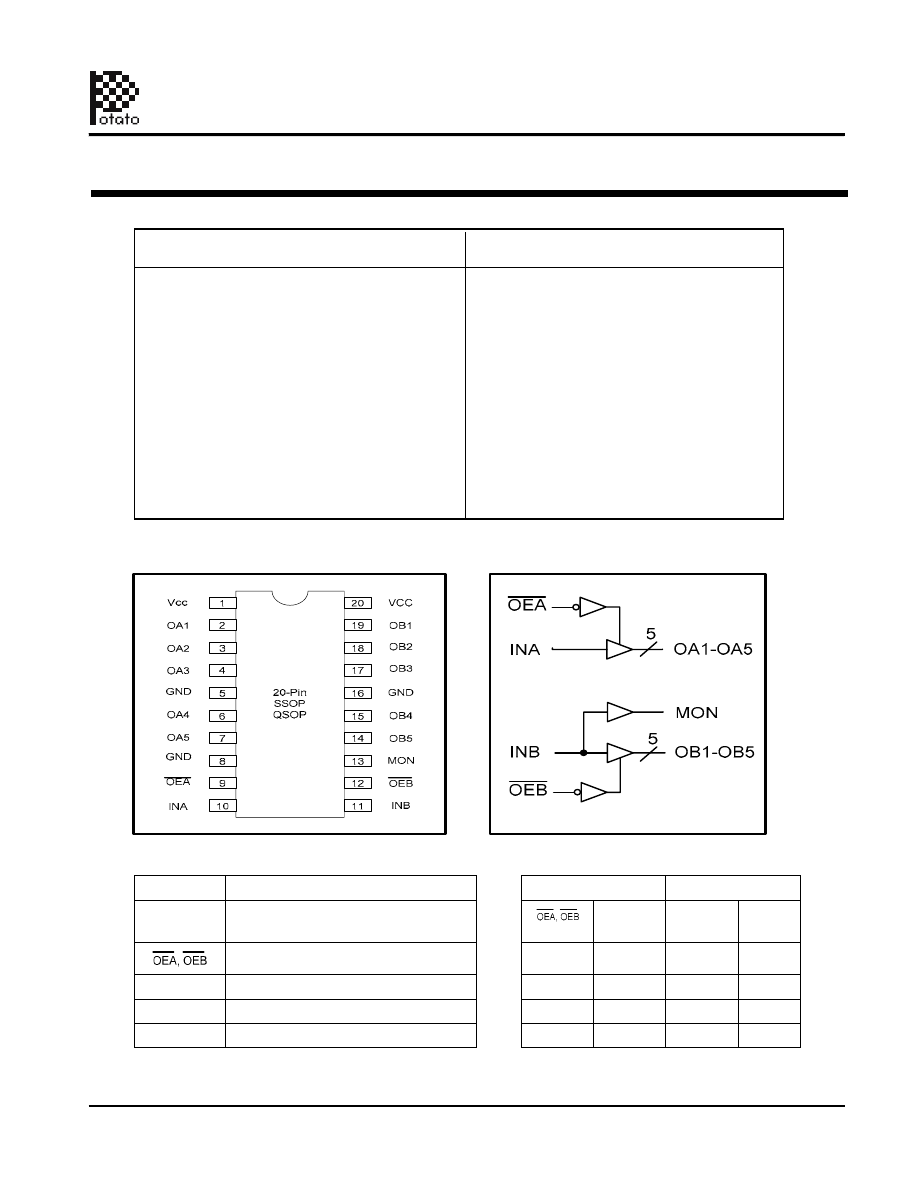
Pin Configuration

Logic Block Diagram

Pin Description

Pin Name

Description

Inputs

Outputs

INA, INB

Signal or clock Inputs

INA, INB

OAn, OBn

MON

Hi-Z State Output Enable Inputs (Active LOW)

L

L

L

L

H

H

H

L

s

t

u

p

t

u

O

k

c

o

l

c

r

o

l

a

n

g

i

S

n

B

O

,

n

A

O

L

Z

L

H

t

u

p

t

u

O

r

o

ti

n

o

M

N

O

M

Vcc, GND

Power, Ground

H

H

Z

H

Inputs can be driven from either 3.3V or 5V devices. 
This feature allows the use of these devices as 
translators in a mixed 3.3V/5V system environment. 

. Patented technology

1.2V - 3.6V  Dual 1:5 CMOS Clock Driver

800MHz TTL/CMOS Potato Chip 

1

01/01/10

Potato Semiconductor Corporation

PO49FCT3805B

www.potatosemi.com

PO49FCT3805B-html.html
background image

Maximum Ratings

DC Electrical Characteristics

Symbol

Description

Test Conditions

Min

Typ

Max

Unit

V

OH

Output High voltage

Vcc=3V Vin=V

IH

or V

IL

, I

OH

= -12mA

2.4

3

-

V

V

OL

Output Low voltage

Vcc=3V Vin=V

IH

or V

IL

, I

OH

=12mA

-

0.3

0.5

V

V

IH

Input High voltage

Guaranteed Logic HIGH Level (Input Pin)

2

-

+5.5

V

V

IL

Input Low voltage

Guaranteed Logic LOW Level (Input Pin)

-0.5

-

0.8

V

I

IH

Input High current

Vcc = 3.6V and Vin = 5.5V

-

-

50

uA

I

OZH

High Impedance
Output current

Vcc = 3.6V and Vo = Vcc

-

-

1

uA

I

OZL

High Impedance
Output current

Vcc = 3.6V and Vo = 0V

-

-

-1

uA

I

IL

Input Low current

Vcc = 3.6V and Vin = 0V

-

-

-50

uA

V

IK

Clamp diode voltage

Vcc = Min. And

I

IN

= -18mA

-

-0.7

-1.2

V

Notes:

1. For conditions shown as Max. or Min., use appropriate value specified under Electrical Characteristics for the applicable device type.
2.

Typical values are at Vcc = 3.3V, 25

°

C ambient.

3.

This parameter is guaranteed but not tested.

4.

Not more than one output should be shorted at one time. Duration of the test should not exceed one second.

5.

VoH = Vcc – 0.6V at rated current

Description

Max

Unit

Storage Temperature

-65 to 150

°

C

Operation Temperature

-40 to 85 

°

C

Operation Voltage

-0.5 to +4.6 

V

Input Voltage

-0.5 to +5.5

V

Output Voltage

-0.5 to Vcc+0.5

V

Note:

stresses greater than listed under
Maximum

Ratings

may

cause

permanent damage to the device. This
is a stress rating only and functional
operation of the device at these or any
other conditions above those indicated
in the operational sections of this
specification is not implied. Exposure
to absolute maximum rating conditions
for extended periods may affect
reliability specification is not implied.

1.2V - 3.6V Dual 1:5 CMOS Clock Driver

800MHz TTL/CMOS Potato Chip 

2

01/01/10

Potato Semiconductor Corporation

PO49FCT3805B

www.potatosemi.com

PO49FCT3805B-html.html
background image

Power Supply Characteristics

Symbol

Description

Test Conditions (1)

Min

Typ

Max

Unit

Icc

Q

Quiescent Power Supply Current

Vcc=Max, Vin=Vcc or GND

-

0.1

30

uA

Notes:

1. For conditions shown as Max. or Min., use appropriate value specified under Electrical Characteristics for the applicable device type.
2. Typical values are at Vcc = 3.3V, 25

°

C ambient.

3. This parameter is guaranteed but not tested.
4. Not more than one output should be shorted at one time. Duration of the test should not exceed one second.

Capacitance (T

A

= +25°C, f= 1MHz)

Parameters (1)

Description

Test Conditions

Typ

Max

Unit

Cin

Input Capacitance

Vin = 0V

3

4

pF

Cout

Output Capacitance

Vout = 0V

-

6

pF

Notes:

1 This parameter is determined by device characterization but not production tested.

Switching Characteristics

Symbol

Description

Test Conditions (1)

Max

Unit

t

PLH &

 t

PHL

Propagation Delay INA to OAn, INB to OBn

CL = 15pF

2.4

ns

t

PZH or

t

PZL

Output Enable Time

CL = 15pF

2.5

ns

t

PHZ or

t

PLZ

Output Disable Time

CL = 15pF

2.5

ns

tr/tf

Rise/Fall Time

0.8V – 2.0V

0.8

ns

tsk(p)

z

H

M

5

2

1

,

F

p

5

1

=

L

C

)

e

g

a

k

c

a

P

e

m

a

S

(

w

e

k

S

e

s

l

u

P

 300

ps

tsk(o)

Output Pin to Pin Skew (Same Package)

CL = 15pF, 125MHz

80 

    ps

tsk(pp)

Output Skew (Different Package)

CL = 15pF, 125MHz

400

ps

fmax

F

p

0

5

=

L

C

y

c

n

e

u

q

e

r

F

t

u

p

n

I

100

MHz

fmax

F

p

5

1

=

L

C

y

c

n

e

u

q

e

r

F

t

u

p

n

I

300

MHz

fmax

F

p

5

=

L

C

y

c

n

e

u

q

e

r

F

t

u

p

n

I

600

MHz

fmax

F

p

2

=

L

C

y

c

n

e

u

q

e

r

F

t

u

p

n

I

800

MHz

Notes:

1. See test circuits and waveforms.
2. tpLH, tpHL, tsk(p), and tsk(o) are production tested. All other parameters guaranteed but not production tested.
3. Airflow of 1m/s is recommended for frequencies above 133MHz

1.2V - 3.6V 1:5 Dual CMOS Clock Driver

800MHz TTL/CMOS Potato Chip 

3

01/01/10

Potato Semiconductor Corporation

PO49FCT3805B

www.potatosemi.com

PO49FCT3805B-html.html
background image

Test Waveforms

Test Circuit

50Ohm

500

500

50Ohm

1.2V - 3.6V Dual 1:5 CMOS Clock Driver

800MHz TTL/CMOS Potato Chip 

4

01/01/10

Potato Semiconductor Corporation

PO49FCT3805B

www.potatosemi.com

PO49FCT3805B-html.html
background image

Packaging Mechanical Drawing: 20 pin QSOP

Packaging Mechanical Drawing: 20 pin SOIC

1.2V - 3.6V Dual 1:5 CMOS Clock Driver

800MHz TTL/CMOS Potato Chip 

5

01/01/10

Potato Semiconductor Corporation

PO49FCT3805B

www.potatosemi.com

PO49FCT3805B-html.html
background image

Packaging Mechanical Drawing: 20 pin SSOP

.272

.295

.078

.002

SEATING

 PLANE

.0098

Max.

.0256

 BSC

1

20

.197

.220

0.25

X.XX

X.XX

DENOTES DIMENSIONS

IN MILLIMETERS

0.050

5.00

5.60

2.00

6.90

7.50

0.65

Max

Min

.022

.037

.004

.009

.291

.322

7.40

8.20

0.55

0.95

0.09

0.25

1.2V - 3.6V Dual 1:5 CMOS Clock Driver

800MHz TTL/CMOS Potato Chip 

6

01/01/10

Potato Semiconductor Corporation

PO49FCT3805B

www.potatosemi.com

IC Ordering Information

Top-Marking

Ordering Code

Package

Pb-free & Green

PO49FCT3805BCU for Tube
PO49FCT3805BCR for Tape & Reel

PO49FCT3805BC
PO49FCT3805BC

-40

°

C to 85

°

C

-40

°

C to 85

°

C

PO49FCT3805BQU for Tube
PO49FCT3805BQR for Tape & Reel

PO49FCT3805BQ
PO49FCT3805BQ

-40

°

C to 85

°

C

-40

°

C to 85

°

C

PO49FCT3805BSSU for Tube
PO49FCT3805BSSR for Tape & Reel

PO49FCT3805BSS
PO49FCT3805BSS

-40

°

C to 85

°

C

-40

°

C to 85

°

C

TA

IC Package Information

PACKAGE

C

24

12

Top Left Corner

26 (12”)

1000

43 (20”)

38

20pin 300mil SOIC

CODE

PACKAGE

TYPE

TAPE

WIDTH

TAPE TRAILER

TUBE

TAPE & REEL

LENGTH

TAPE

PITCH

QTY

LENGTH

TAPE LEADER

PER TAPE

QTY
PER

PIN 1 LOCATION

(mm)

(mm)

Q

16

8

Top Left Corner

39 (12”)

3000

64 (20”)

55

20pin 150mil QSOP

SS

16

12

Top Left Corner

26 (12”)

2000

43 (20”)

66

20pin 209mil SSOP

Pb-free & Green

20pin 300mil SOIC

20pin 300mil SOIC

20pin 150mil QSOP

20pin 150mil QSOP

Pb-free & Green

Pb-free & Green

Pb-free & Green

Pb-free & Green

20pin 209mil SSOP

20pin 209mil SSOP