background image

1


400MHz TTL/CMOS Potato Chip 

 PO49HSTL3807G 

3.3V 1:10 Differential to TTL Translator Driver 

FEATURES: 

DESCRIPTION: 

. Operating frequency up to 400MHz with 2pf load 
. Operating frequency up to 300MHz with 5pf load 
. Operating frequency up to 250MHz with 15pf load 
. Operating frequency up to 120MHz with 50pf load 
. Very low output pin to pin skew < 350ps 
. Very low pulse skew < 100ps 
. VCC = 1.65V to 3.6V 
. Propagation delay < 2.7ns max with 15pf load 
. Low input capacitance: 3pf typical 
. 1:10 fanout 
. Available in 20pin 150mil wide QSOP package 
. Available in 20pin 300mil wide SOIC package 

Potato  Semiconductor’s  PO49HSTL3807G  is 
designed  for  world  top  performance  using 
submicron  CMOS  technology  to  achieve 
400MHz  TTL  output  frequency  with  less  than 
100ps output pulse skew.  

PO49HSTL3807G  is  a  1.65v  to  3.6V  1  high 
speed  comparator  inputs  to  10  TTL  output 
buffered  driver  to  achieve  higher  than  400MHz 
output frequency. Typical applications are HSTL, 
PECL,  LVDS  to  TTL  translator,  crystal  or  ring 
oscillator, clock and signal distribution. 
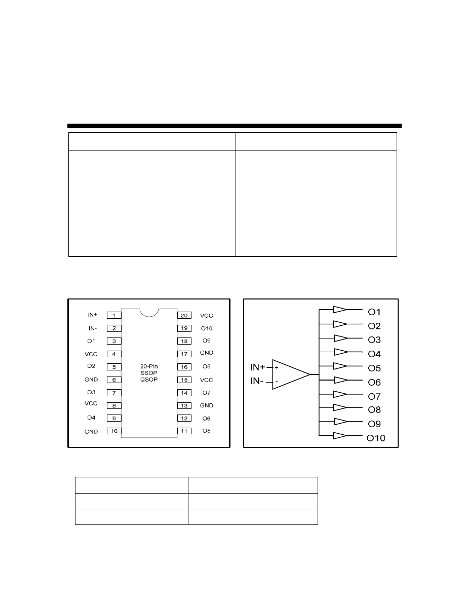
Pin Configuration


Logic Block Diagram

Pin Description

Pin Name

Description


s

t

u

p

n

I


-

N

I

 ,

+

N

I

O1 to O10 

Outputs

PO49HSTL3807G-html.html
background image


2

400MHz TTL/CMOS Potato Chip 


PO49HSTL3807G 

3.3V 1:10 Differential to TTL Translator Driver 


Maximum Ratings


DC Electrical Characteristics 


Symbol  Description 

Test 

Conditions 

Min   

Typ Max  Unit 

V

OH


Output High voltage


Vcc=3V Vin=V

IH

 or V

IL

, I

OH

= -12mA


2.4 3  -  V 

V

OL


Output Low voltage


Vcc=3V Vin=V

IH

 or V

IL

, I

OH

=12mA


- 0.3 0.5 V 

V

IH


Input High voltage


Guaranteed Logic HIGH Level (Input Pin)


2 - 

Vcc 

V

IL


Input Low voltage


Guaranteed Logic LOW Level (Input Pin)


-0.5 -  0.8 V 

I

IH


Input High current


Vcc = 3.6V and Vin = 3.6V 

- - 1 

uA 

I

IL


Input Low current


Vcc = 3.6V and Vin = 0V 

- - -1 

uA 

V

IK


Clamp diode voltage


Vcc = Min. And 

I

IN 

= -18mA 

- -0.7 

-1.2 V 


Notes: 

1.


For conditions shown as Max. or Min., use appropriate value specified under Electrical Characteristics for the applicable device type. 

2.


Typical values are at Vcc = 3.3V, 25 

°

C ambient.


3.


This parameter is guaranteed but not tested.


4.


Not more than one output should be shorted at one time.  Duration of the test should not exceed one second.


5.


VoH = Vcc – 0.6V at rated current   


Description Max 

Unit 

Storage Temperature 

-65 to 150 

°

Operation Temperature 

-40 to 85 

°

Operation Voltage 

-0.5 to +4.6 

Input Voltage 

-0.5 to Vcc+0.5 

Output Voltage 

-0.5 to Vcc+0.5 

Note:


stresses greater than listed under 
Maximum Ratings may cause 
permanent damage to the device. This 
is a stress rating only and functional 
operation of the device at these or any 
other conditions above those indicated 
in the operational sections of this 
specification is not implied. Exposure 
to absolute maximum rating conditions 
for extended periods may affect 
reliability specification is not implied.


PO49HSTL3807G-html.html
background image


3

400MHz TTL/CMOS Potato Chip 


PO49HSTL3807G 

3.3V 1:10 Differential to TTL Translator Driver 


Power Supply Characteristics 


Symbol 

Description 

Test Conditions (1) 

Min 

Typ 

Max 

Unit 

Icc

Q


Quiescent Power Supply Current


Vcc=Max,  Vin=Vcc or GND

- 0.1 30 uA 

Icc 

Power Supply Current per Input High


Vcc=Max,  Vin= Vcc-0.6V

- 50 300 

uA 

Notes: 

1.


For conditions shown as Max. or Min., use appropriate value specified under Electrical Characteristics for the applicable device type. 

2.


Typical values are at Vcc = 3.3V, 25

°

C ambient. 

3.


This parameter is guaranteed but not tested. 

4.


Not more than one output should be shorted at one time.  Duration of the test should not exceed one second. 

5.


VoH = Vcc – 0.6V at rated current


Capacitance 

Parameters (1) 


Description 

Test Conditions 

 Typ 

Max 

Unit 

Cin 

Input Capacitance


Vin = 0V


3 4 pF

Cout 

Output Capacitance


Vout = 0V


- 6 pF

Notes: 

1


This parameter is determined by device characterization but not production tested. 


Switching Characteristics 


Symbol 


Description 

Test Conditions (1) 

Max 

Unit 

t

PLH 

Propagation Delay A to Bn


CL = 15pF


2.7 ns 

t

PHL 

Propagation Delay A to Bn


CL = 15pF


2.7 ns 

tr/tf 

Rise/Fall Time


0.8V – 2.0V


0.8 ns 

tsk(p) 

Pulse Skew (Same Package) 

CL = 15pF,V+ = 125MHz, V- = 1.5v 

0.1 ns 

tsk(o) 

Output Pin to Pin Skew (Same Package) 

CL = 15pF,V+ = 125MHz, V- = 1.5v 

0.35 ns 

tsk(pp) 

Output Skew (Different Package) 

CL = 15pF,V+ = 125MHz, V- = 1.5v 

0.4 ns 

fmax 

Input Frequency 

CL = 50pF 

120 MHz 

fmax 

Input Frequency 

CL =15pF 

250 MHz 

fmax 

Input Frequency 

CL = 5pF 

300 MHz 

fmax 

Input Frequency 

CL = 2pF 

400 MHz 

Notes: 

1.


See test circuits and waveforms. 

2.


tpLH, tpHL, tsk(p), and tsk(o) are production tested.  All other parameters guaranteed but not production tested. 

3.


Airflow of 1m/s is recommended for frequencies above 133MHz 


PO49HSTL3807G-html.html
background image


4

400MHz TTL/CMOS Potato Chip 


PO49HSTL3807G 

3.3V 1:10 Differential to TTL Translator Driver 


Test Waveforms


Test Circuit 

50

50


PO49HSTL3807G-html.html
background image


5

400MHz TTL/CMOS Potato Chip 


PO49HSTL3807G 

3.3V 1:10 Differential to TTL Translator Driver 


Packaging Mechanical Drawing: 20 pin QSOP


Packaging Mechanical Drawing: 20 pin SOIC