background image

FEATURES:

. Patented technology
. Operating frequency up to 1.125GHz with 2pf load
. Operating frequency up to 550MHz with 5pf load
. Operating frequency up to 300MHz with 15pf load
. VCC Operates from 1.65V to 3.6V
. Propagation delay < 1.5ns max with 15pf load
. Low input capacitance: 4pf typical
. Available in 14pin 150mil wide SOIC package
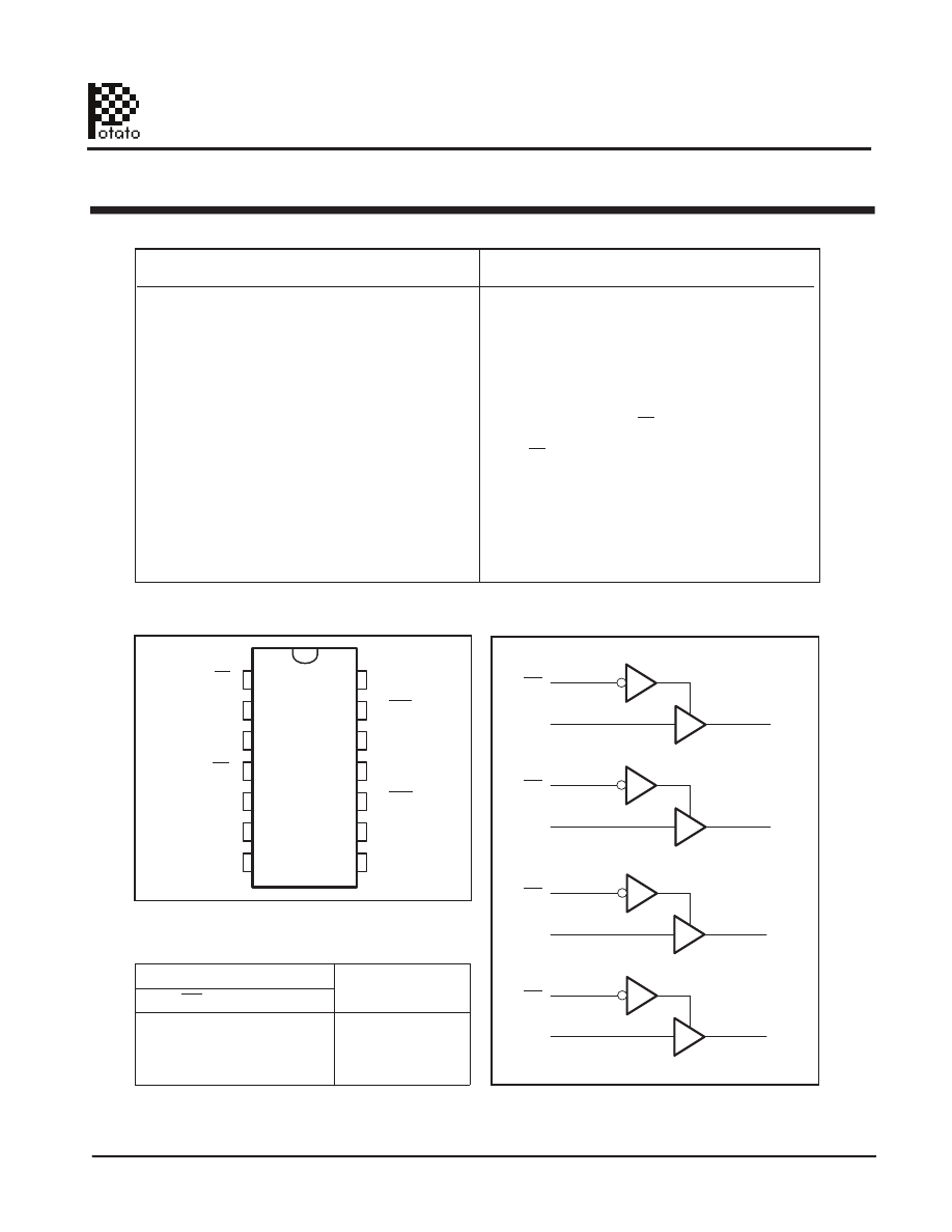
Pin Configuration

Logic Block Diagram

Pin Description

1
2
3
4
5
6
7

14
13
12

11

10

9
8

DESCRIPTION:

Potato Semiconductor’s PO74G125A is designed for 

world top performance using submicron CMOS 

technology to achieve 1.125GHz TTL /CMOS output 

frequency with less than 1.5ns propagation delay.

This quadruple bus buffer gate is designed for 1.65-V 

to 3.6-V V

CC

 operation.

The

PO74G125A

features independent line drivers with 

3-state outputs. Each output is disabled when the 

associated output-enable (OE) input is high. To ensure 

the high-impedance state during power up or power 

down, OE should be tied to V

CC

 through a pullup 

resistor; the minimum value of the resistor is 

determined by the current-sinking capability of 

the driver.

Inputs can be driven from either 3.3V or 5V devices. 

This feature allows the use of these devices as 

translators in a mixed 3.3V/5V system environment.

1OE

1A
1Y

2OE

2A
2Y

GND

V

CC

4OE
4A
4Y
3OE
3A
3Y

INPUTS

OUTPUT

Y

OE

A

L

H

H

L

L

L

H

X

Z

10

3OE

9

3A

3Y

8

13

4OE

12

4A

4Y

11

1

1OE

2

1A

1Y

3

4

2OE

5

2A

2Y

6

  74 Series Noise Cancellation GHz Logic 

1

01/01/10

Potato Semiconductor Corporation

PO74G125A

www.potatosemi.com

QUADRUPLE BUS BUFFER GATES

WITH 3-STATE OUTPUTS

PO74G125A-html.html
background image

Maximum Ratings

DC Electrical Characteristics

Symbol

Description

Test Conditions

Min

Typ

Max

Unit

V

OH

Output High voltage

Vcc=3V Vin=V

IH

or V

IL

, I

OH

= -12mA

2.4

3

-

V

V

OL

Output Low voltage

Vcc=3V Vin=V

IH

or V

IL

, I

OH

=12mA

-

0.3

0.5

V

V

IH

Input High voltage

Guaranteed Logic HIGH Level (Input Pin)

2

-

5.5

V

V

IL

Input Low voltage

Guaranteed Logic LOW Level (Input Pin)

-0.5

-

0.8

V

I

IH

Input High current

Vcc = 3.6V and Vin = 5.5V

-

-

1

uA

I

IL

Input Low current

Vcc = 3.6V and Vin = 0V

-

-

-1

 uA 

V

IK

Clamp diode voltage

Vcc = Min. And

I

IN

= -18mA

-

-0.7

-1.2

V

Notes:

1. For conditions shown as Max. or Min., use appropriate value specified under Electrical Characteristics for the applicable device type.
2.

Typical values are at Vcc = 3.3V, 25

°

C ambient.

3.

This parameter is guaranteed but not tested.

4.

Not more than one output should be shorted at one time. Duration of the test should not exceed one second.

5.

VoH = Vcc – 0.6V at rated current

Description

Max

Unit

Storage Temperature

-65 to 150

°

C

Operation Temperature

-40 to 125 

°

C

Operation Voltage

-0.5 to +4.6 

V

Input Voltage

-0.5 to +5.5

V

Output Voltage

-0.5 to Vcc+0.5

V

Note:

stresses greater than listed under
Maximum

Ratings

may

cause

permanent damage to the device. This
is a stress rating only and functional
operation of the device at these or any
other conditions above those indicated
in the operational sections of this
specification is not implied. Exposure
to absolute maximum rating conditions
for extended periods may affect
reliability specification is not implied.

  74 Series Noise Cancellation GHz Logic 

2

01/01/10

Potato Semiconductor Corporation

PO74G125A

www.potatosemi.com

QUADRUPLE BUS BUFFER GATES

WITH 3-STATE OUTPUTS

PO74G125A-html.html
background image

Power Supply Characteristics

Symbol

Description

Test Conditions (1)

Min

Typ

Max

Unit

Icc

Q

Quiescent Power Supply Current

Vcc=Max, Vin=Vcc or GND

-

0.1

30

uA

Icc

Power Supply Current per Input High

Vcc=Max, Vin= Vcc-0.6V

-

50

300

uA

Notes:

1. For conditions shown as Max. or Min., use appropriate value specified under Electrical Characteristics for the applicable device type.
2. Typical values are at Vcc = 3.3V, 25

°

C ambient.

3. This parameter is guaranteed but not tested.
4. Not more than one output should be shorted at one time. Duration of the test should not exceed one second.
5. VoH = Vcc – 0.6V at rated current

Capacitance

Parameters (1)

Description

Test Conditions

Typ

Unit

Cin

Input Capacitance

Vin = 0V

4

pF

Cout

Output Capacitance

Vout = 0V

6

pF

Notes:

1 This parameter is determined by device characterization but not production tested.

Switching Characteristics

t

i

n

U

x

a

M

)

1

(

s

n

o

i

t

i

d

n

o

C

t

s

e

T

n

o

i

t

p

i

r

c

s

e

D

l

o

b

m

y

S

t

PLH

Propagation Delay A to Y

CL = 15pF

1.5

ns

t

PHL

Propagation Delay A to Y

CL = 15pF

1.5

ns

tr/tf

Rise/Fall Time

0.8V – 2.0V

0.8

ns

fmax

F

p

5

1

=

L

C

y

c

n

e

u

q

e

r

F

t

u

p

n

I

300

MHz

fmax

F

p

5

=

L

C

y

c

n

e

u

q

e

r

F

t

u

p

n

I

550

MHz

fmax

F

p

2

=

L

C

y

c

n

e

u

q

e

r

F

t

u

p

n

I

1125

MHz

Notes:

1. See test circuits and waveforms.
2. tpLH, tpHL, tsk(p), and tsk(o) are production tested. All other parameters guaranteed but not production tested.
3. Airflow of 1m/s is recommended for frequencies above 133MHz

t

PZH or

t

PZL

Output Enable Time

CL = 15pF

CL = 15pF

2.5

ns

2.5

ns

t

PHZ or

t

PLZ

Output Disable Time

  74 Series Noise Cancellation GHz Logic 

3

01/01/10

Potato Semiconductor Corporation

PO74G125A

www.potatosemi.com

QUADRUPLE BUS BUFFER GATES

WITH 3-STATE OUTPUTS

PO74G125A-html.html
background image

Test Waveforms

Test Circuit

50Ohm

50Ohm

500

500Ohm

15pF
to
2pF

  74 Series Noise Cancellation GHz Logic 

4

01/01/10

Potato Semiconductor Corporation

PO74G125A

www.potatosemi.com

QUADRUPLE BUS BUFFER GATES

WITH 3-STATE OUTPUTS

PO74G125A-html.html
background image

Packaging Mechanical Drawing: 14 pin 150mil SOIC

Denotes dimensions in inches

Denotes dimensions in millimenters

X.XX
X.XX

X.XX
X.XX

0.010
0.007

0.25
0.17

0.050
0.016

1.27
0.40

0.244
0.228

6.20
5.80

  74 Series Noise Cancellation GHz Logic 

5

01/01/10

Potato Semiconductor Corporation

PO74G125A

www.potatosemi.com

Top-Marking

IC Ordering Information

Ordering Code

Package

14pin 150mil SOIC 

Pb-free & Green

14pin 150mil SOIC 

Pb-free & Green

PO74G125ASU for Tube

POTATO74G125AS
POTATO74G125AS

PO74G125ASR for Tape & Reel

-40 C to
-40 C to 125 C

TA

IC Package Information

PACKAGE
CODE

PACKAGE
TYPE

QTY
PER
TUBE

TAPE
WIDTH
(mm)

TAPE
PITCH
(mm)

PIN 1  LOCATION

TAPE TRAILER 
LENGTH

QTY
PER REEL

TAPE LEADER 
LENGTH

S

SOIC 14

16

8

Top Left Corner

39 (12”)

3000

64 (20”)

55

125 C

QUADRUPLE BUS BUFFER GATES

WITH 3-STATE OUTPUTS