FEATURES:
. Patented technology
. Operating frequency up to 1.125GHz with 2pf load
. Operating frequency up to 800MHz with 5pf load
. Operating frequency up to 350MHz with 15pf load
. VCC Operates from 1.65V to 3.6V
. Propagation delay < 1.7ns max with 15pf load
. Low input capacitance: 4pf typical
. Available in 16 pin SOIC package
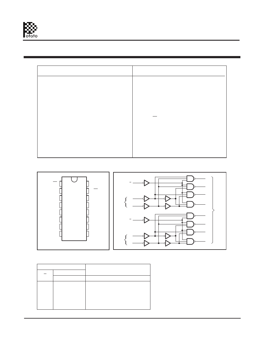
Pin Configuration
Logic Block Diagram
Pin Description
DESCRIPTION:
Potato Semiconductor’s PO74G139A is designed for
world top performance using submicron CMOS
technology to achieve 1.125GHz TTL /CMOS output
frequency with less than 1.7ns propagation delay.
This quadruple bus buffer gate is designed for 1.65-V
to 3.6-V V
CC
operation.
The
PO74G139A
comprises two individual 2-line to
4-line decoders in a single package. Theactive-
lowenable (G) input can be used as a data line in
demultiplexing applications. This decoder/ demulti-
plexer features fully buffered
inputs, each of which represents only one normalized-
load to itsdriving circuit.
Inputs can be driven from either 3.3V or 5V devices.
This feature allows the use of these devices as
translators in a mixed 3.3V/5V system environment.
1
2
3
4
5
6
7
8
16
15
14
13
12
11
10
9
1G
1A
1B
1Y0
1Y1
1Y2
1Y3
GND
V
CC
2G
2A
2B
2Y0
2Y1
2Y2
2Y3
Select
Inputs
Select
Inputs
2B
2A
2G
1B
1A
1G
Data
Outputs
2Y3
2Y2
2Y1
2Y0
1Y3
1Y2
1Y1
1Y0
1
2
3
15
14
13
4
5
6
7
12
11
10
9
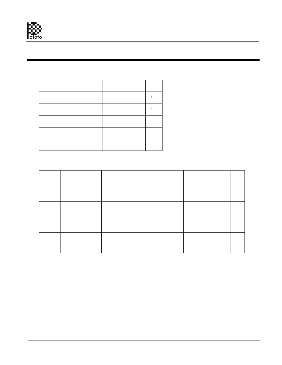
INPUTS
OUTPUTS
SELECT
G
B
A
Y3
Y2
Y1
Y0
L
L
L
H
H
H
L
L
L
H
H
H
L
H
L
H
L
H
L
H
H
L
H
H
L
H
H
H
H
X
X
H
H
H
H
DUAL2-LINETO4-LINEDECODER/DEMULTIPLEXER
74 Series Noise Cancellation GHz Logic
1
01/01/10
Potato Semiconductor Corporation
PO74G139A
www.potatosemi.com
PO74G139A-html.html
Maximum Ratings
DC Electrical Characteristics
Symbol
Description
Test Conditions
Min
Typ
Max
Unit
V
OH
Output High voltage
Vcc=3V Vin=V
IH
or V
IL
, I
OH
= -12mA
2.4
3
-
V
V
OL
Output Low voltage
Vcc=3V Vin=V
IH
or V
IL
, I
OH
=12mA
-
0.3
0.5
V
V
IH
Input High voltage
Guaranteed Logic HIGH Level (Input Pin)
2
-
5.5
V
V
IL
Input Low voltage
Guaranteed Logic LOW Level (Input Pin)
-0.5
-
0.8
V
I
IH
Input High current
Vcc = 3.6V and Vin = 5.5V
-
-
1
uA
I
IL
Input Low current
Vcc = 3.6V and Vin = 0V
-
-
-1
uA
V
IK
Clamp diode voltage
Vcc = Min. And
I
IN
= -18mA
-
-0.7
-1.2
V
Notes:
1. For conditions shown as Max. or Min., use appropriate value specified under Electrical Characteristics for the applicable device type.
2.
Typical values are at Vcc = 3.3V, 25
°
C ambient.
3.
This parameter is guaranteed but not tested.
4.
Not more than one output should be shorted at one time. Duration of the test should not exceed one second.
5.
VoH = Vcc – 0.6V at rated current
Description
Max
Unit
Storage Temperature
-65 to 150
°
C
Operation Temperature
-40 to 125
°
C
Operation Voltage
-0.5 to +4.6
V
Input Voltage
-0.5 to +5.5
V
Output Voltage
-0.5 to Vcc+0.5
V
Note:
stresses greater than listed under
Maximum
Ratings
may
cause
permanent damage to the device. This
is a stress rating only and functional
operation of the device at these or any
other conditions above those indicated
in the operational sections of this
specification is not implied. Exposure
to absolute maximum rating conditions
for extended periods may affect
reliability specification is not implied.
DUAL2-LINETO4-LINEDECODER/DEMULTIPLEXER
74 Series Noise Cancellation GHz Logic
2
01/01/10
Potato Semiconductor Corporation
PO74G139A
www.potatosemi.com
PO74G139A-html.html
Power Supply Characteristics
Symbol
Description
Test Conditions (1)
Min
Typ
Max
Unit
Icc
Q
Quiescent Power Supply Current
Vcc=Max, Vin=Vcc or GND
-
0.1
30
uA
Icc
Power Supply Current per Input High
Vcc=Max, Vin= Vcc-0.6V
-
50
300
uA
Notes:
1. For conditions shown as Max. or Min., use appropriate value specified under Electrical Characteristics for the applicable device type.
2. Typical values are at Vcc = 3.3V, 25
°
C ambient.
3. This parameter is guaranteed but not tested.
4. Not more than one output should be shorted at one time. Duration of the test should not exceed one second.
5. VoH = Vcc – 0.6V at rated current
Capacitance
Parameters (1)
Description
Test Conditions
Typ
Unit
Cin
Input Capacitance
Vin = 0V
4
pF
Cout
Output Capacitance
Vout = 0V
6
pF
Notes:
1 This parameter is determined by device characterization but not production tested.
Switching Characteristics
t
i
n
U
x
a
M
)
1
(
s
n
o
i
t
i
d
n
o
C
t
s
e
T
n
o
i
t
p
i
r
c
s
e
D
l
o
b
m
y
S
t
PLH
Propagation Delay A, B to Y
CL = 15pF
1.7
ns
t
PHL
Propagation Delay A, B to Y
CL = 15pF
1.7
ns
tr/tf
Rise/Fall Time
0.8V – 2.0V
0.8
ns
fmax
F
p
5
1
=
L
C
y
c
n
e
u
q
e
r
F
t
u
p
n
I
350
MHz
fmax
F
p
5
=
L
C
y
c
n
e
u
q
e
r
F
t
u
p
n
I
800
MHz
fmax
F
p
2
=
L
C
y
c
n
e
u
q
e
r
F
t
u
p
n
I
1125
MHz
Notes:
1. See test circuits and waveforms.
2. tpLH, tpHL, tsk(p), and tsk(o) are production tested. All other parameters guaranteed but not production tested.
3. Airflow of 1m/s is recommended for frequencies above 133MHz
tsk(o)
Output Pin to Pin Skew
CL = 15pF, 125MHz
0.25
ns
DUAL2-LINETO4-LINEDECODER/DEMULTIPLEXER
74 Series Noise Cancellation GHz Logic
3
01/01/10
Potato Semiconductor Corporation
PO74G139A
www.potatosemi.com
PO74G139A-html.html
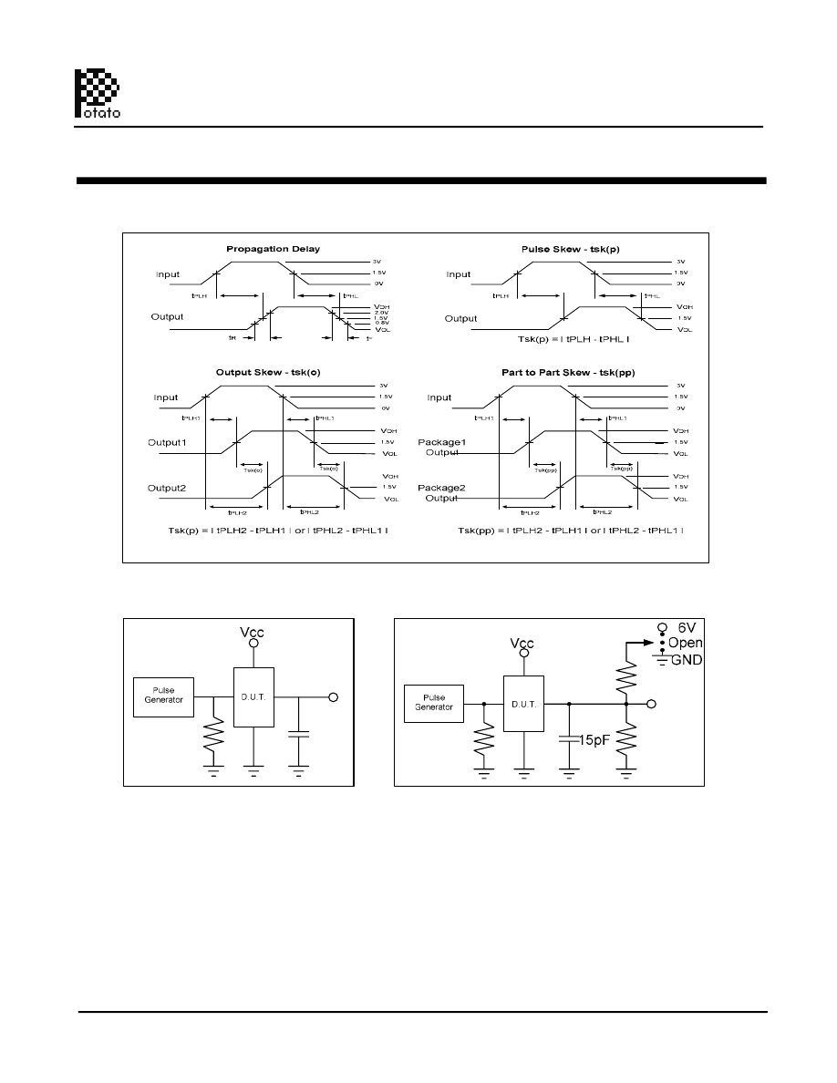
Test Waveforms
Test Circuit
50Ohm
50Ohm
•
500
500Ohm
15pF
to
2pF
DUAL2-LINETO4-LINEDECODER/DEMULTIPLEXER
74 Series Noise Cancellation GHz Logic
4
01/01/10
Potato Semiconductor Corporation
PO74G139A
www.potatosemi.com
PO74G139A-html.html
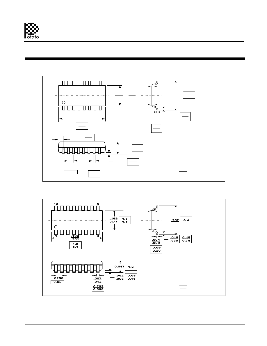
Packaging Mechanical Drawing: 16 pin SOIC
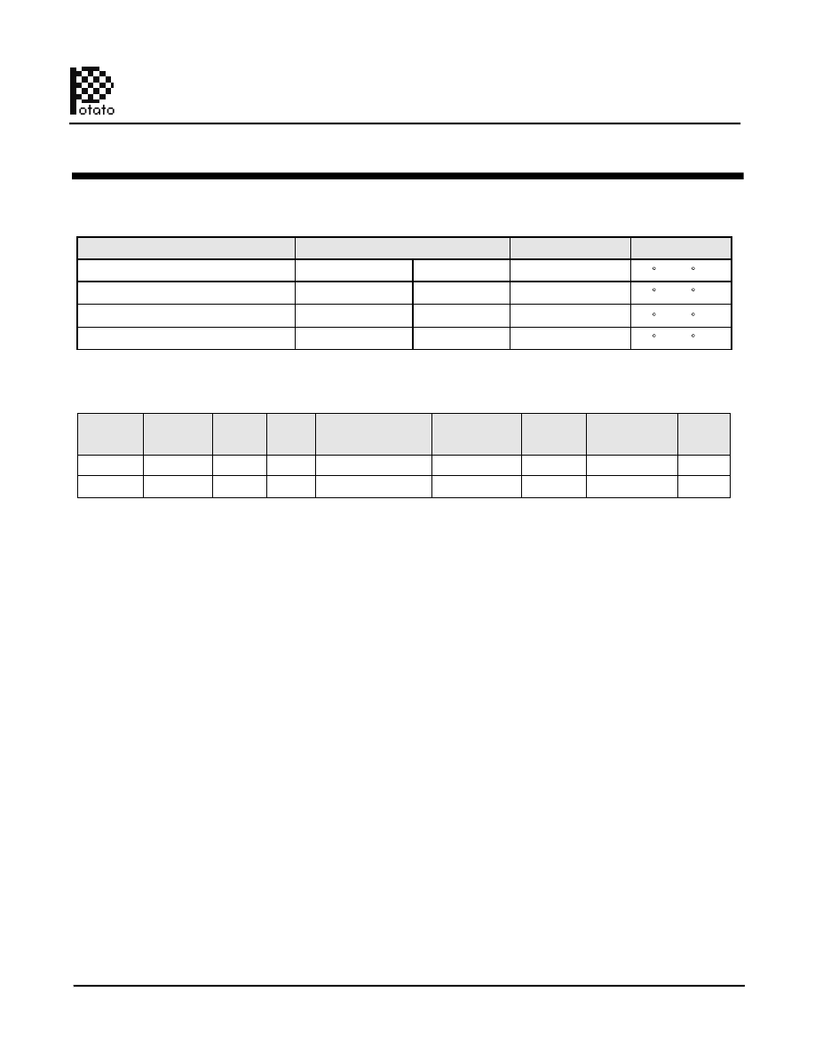
Packaging Mechanical Drawing: 16 pin TSSOP
.050
BSC
1
16
.149
.157
3.78
3.99
.386
.393
9.80
10.00
1.27
.053
.068
1.35
1.75
.0040
.0098
0.10
0.25
.013
.020
.0155
.0260
0.330
0.508
0.393
0.660
.0075
.0098
0.19
0.25
.016
.050
0.41
1.27
.2284
.2440
5.80
6.20
X.XX
X.XX
DENOTES DIMENSIONS
IN MILLIMETERS
X.XX
X.XX
DENOTES DIMENSIONS
IN MILLIMETERS
DUAL2-LINETO4-LINEDECODER/DEMULTIPLEXER
74 Series Noise Cancellation GHz Logic
5
01/01/10
Potato Semiconductor Corporation
PO74G139A
www.potatosemi.com
PO74G139A-html.html
DUAL2-LINETO4-LINEDECODER/DEMULTIPLEXER
IC Ordering Information
Top-Marking
Ordering Code
Package
Pb-free & Green
PO74G139ASU for Tube
PO74G139ASR for Tape & Reel
POTATO74G139AS
POTATO74G139AS
-40 C to 85 C
-40 C to 85 C
173mil TSSOP 16
PO74G139ATU for Tube
PO74G139ATR for Tape & Reel
POTATO74G139AT
POTATO74G139AT
-40 C to 85 C
-40 C to 85 C
TA
IC Package Information
PACKAGE
CODE
PACKAGE
TYPE
QTY
PER
TUBE
TAPE
WIDTH
(mm)
TAPE
PITCH
(mm)
PIN 1 LOCATION
TAPE TRAILER
LENGTH
QTY
PER REEL
TAPE LEADER
LENGTH
S
SOIC 16
16
8
Top Left Corner
39 (12”)
3000
64 (20”)
48
T
TSSOP 16
12
8
Top Left Corner
39 (12”)
3000
64 (20”)
96
Pb-free & Green
Pb-free & Green
Pb-free & Green
173mil TSSOP 16
150mil SOIC 16
150mil SOIC 16
74 Series Noise Cancellation GHz Logic
6
01/01/10
Potato Semiconductor Corporation
PO74G139A
www.potatosemi.com