FEATURES:
. Patented technology
. Operating frequency up to 1.125GHz with 2pf load
. Operating frequency up to 700MHz with 5pf load
. Operating frequency up to 300MHz with 15pf load
. Operating frequency up to 100MHz with 50pf load
. VCC Operates from 1.65V to 3.6V
. Propagation delay < 1.5ns max with 15pf load
. Low input capacitance: 4pf typical
. Available in 48pin TSSOP package
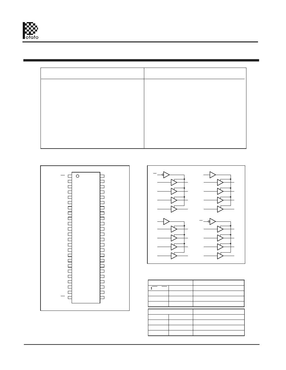
Pin Configuration
Logic Block Diagram
Truth Table
DESCRIPTION:
Potato Semiconductor’s PO74G16241A is designed for
world top performance using submicron CMOS
technology to achieve 1.125GHz TTL /CMOS output
frequency with less than 1.5ns propagation delay.
This Octal bus buffer gate is designed for 1.65-V to
3.6-V V
CC
operation.
The
PO74G16241A
features independent line driver
swith 3-state outputs. Each output is disabled when the
associated output- enable input is high or low.
Inputs can be driven from either 3.3V or 5V devices.
This feature allows the use of these devices as
translators in a mixed 3.3V/5V system environment.
3
Y
1
3
Y
2
3
Y
3
3
Y
4
2
Y
1
2
Y
2
2
Y
3
2
Y
4
4
Y
1
4
Y
2
4
Y
3
4
Y
4
1
Y
2
1
Y
3
1
Y
4
1
Y
1
1
OE
1
A
1
1
A
2
1
A
3
1
A
4
3
OE
3
A
1
3
A
2
3
A
3
3
A
4
2
OE
2
A
1
2
A
2
2
A
3
2
A
4
4
OE
4
A
1
4
A
2
4
A
3
4
A
4
43
44
46
47
1
37
38
40
41
48
12
11
9
8
6
5
3
2
32
33
35
36
25
17
16
14
13
26
27
29
30
24
23
22
20
19
1
2
3
4
5
6
7
8
9
48
10
47
11
46
12
45
13
44
14
43
15
42
16
41
17
40
18
39
19
38
20
37
21
36
22
35
23
34
24
33
32
31
30
29
28
27
26
25
1
OE
1
Y
1
1
Y
2
GND
1
Y
3
1
Y
4
V
CC
2
Y
1
2
Y
2
GND
2
Y
3
2
Y
4
3
Y
1
3
Y
2
GND
3
Y
3
3
Y
4
V
CC
4
Y
1
4
Y
2
GND
4
Y
3
4
Y
4
4
OE
2
OE
1
A
1
1
A
2
GND
1
A
3
1
A
4
V
CC
2
A
1
2
A
2
GND
2
A
3
2
A
4
3
A
1
3
A
2
GND
3
A
3
3
A
4
V
CC
4
A
1
4
A
2
GND
4
A
3
4
A
4
3
OE
s
t
u
p
n
s
I
t
u
p
t
u
O
s
t
u
p
n
s
I
t
u
p
t
u
O
E
O
4
,
E
O
1A, 4A
1Y, 4Y
H
H
H
H
H
L
H
H
L
L
L
L
L
Z
X
X
Z
L
2Y, 3Y
2A, 3A
2OE, 3OE
16-BIT BUFFERS/ DRIVERS WITH 3-STATE OUTPUTS
74 Series Noise Cancellation GHz Logic
1
01/01/10
Potato Semiconductor Corporation
PO74G16241A
www.potatosemi.com