FEATURES:
. Patented technology
. Operating frequency up to 1GHz with 2pf load
. Operating frequency up to 730MHz with 5pf load
. Operating frequency up to 320MHz with 15pf load
. Operating frequency up to 75MHz with 50pf load
. VCC Operates from 1.2V to 3.6V
. Propagation delay < 1.65ns max with 15pf load
. Low input capacitance: 5pf typical
. Available in 48pin TSSOP package
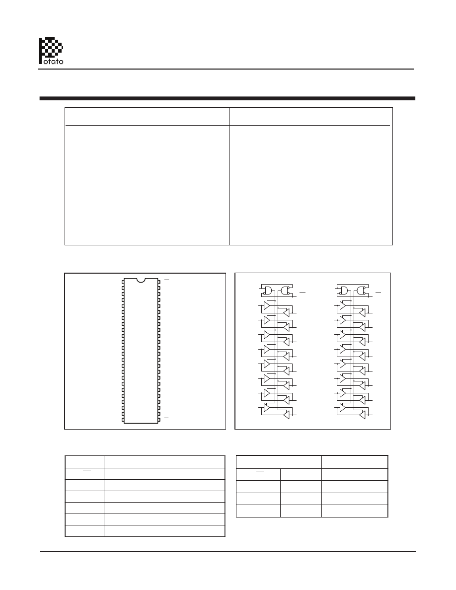
Pin Configuration
Logic Block Diagram
Pin Description
Truth Table
DESCRIPTION:
Potato Semiconductor’s PO74G16245B is designed for
world top performance using submicron CMOS
technology to achieve 1GHz TTL /CMOS output
frequency with less than 1.65ns propagation delay.
This Octal bus buffer gate is designed for 1.2-V to
3.6-V V
CC
operation.
The
PO74G16245B
features independent 16-bit
Bidirectional Transceiver with 3 state outputs. Each
output is disabled when the associated output-
enable(OE) input is high.
E
O
2
E
O
1
1B0
1A0
1DIR
1B1
1A1
1B2
1A2
1B3
1A3
1B4
1A4
1B5
1A5
1B6
1A6
1B7
1A7
2B0
2A0
2DIR
2B1
2A1
2B2
2A2
2B3
2A3
2B4
2A4
2B5
2A5
2B6
2A6
2B7
2A7
1DIR
1B0
1B1
GND
1B2
1B3
VCC
1B4
1B5
GND
1B6
1B7
2B0
2B1
GND
2B2
2B3
VCC
2B4
2B5
GND
2B6
2B7
2DIR
1OE
1A0
1A1
GND
1A2
1A3
VCC
1A4
1A5
GND
1A6
1A7
2A0
2A1
GND
2B2
2A3
VCC
2A4
2A5
GND
2A6
2A7
2OE
48
47
46
45
44
43
42
41
40
39
38
37
36
35
34
33
32
31
30
29
28
27
26
25
1
2
3
4
5
6
7
8
9
10
11
12
13
14
15
16
17
18
19
20
21
22
23
24
e
m
a
N
n
i
P
n
o
i
t
p
i
r
c
s
e
D
O
)
E
x
W
O
L
e
v
it
c
A
(
s
t
u
p
n
I
e
l
b
a
n
E
t
u
p
t
u
O
e
t
a
t
S
-
3
R
I
D
t
x
u
p
n
I
l
o
r
t
n
o
C
n
o
it
c
e
ri
D
X
A
X
s
t
u
p
n
I
e
t
a
t
S
-
3
r
o
s
t
u
p
n
I
A
e
d
i
S
X
B
X
s
t
u
p
t
u
O
e
t
a
t
S
-
3
r
o
s
t
u
p
t
u
O
B
e
d
i
S
D
N
G
d
n
u
o
r
G
V
C
C
r
e
w
o
P
s
t
u
p
n
s
I
t
u
p
t
u
O
E
O
x
R
I
D
x
A
L
L
s
u
B
o
t
a
t
a
D
B
s
u
B
B
H
L
s
u
B
o
t
a
t
a
D
A
s
u
B
H
X
Z
1.2v-3.6v, 16-bit Bidirectional Transceiver with 3 state outputs
74 Series Noise Cancellation GHz Logic
1
01/01/10
Potato Semiconductor Corporation
PO74G16245B
www.potatosemi.com