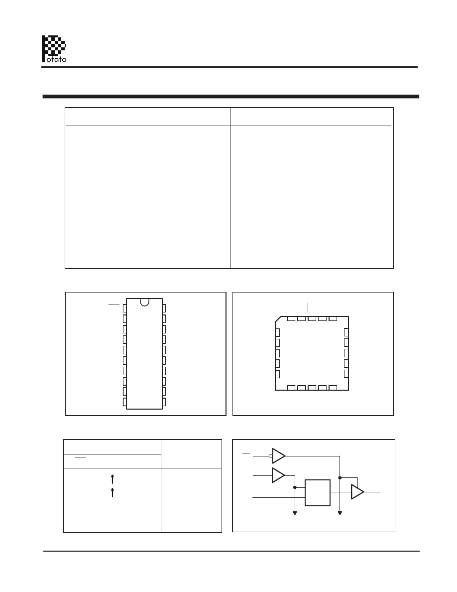
background image

FEATURES:

Pin Configuration

Logic Block Diagram

Pin Description

DESCRIPTION:

Potato Semiconductor’s PO74G374A is designed for 

world top performance using submicron CMOS 
technology to achieve higher than 

600MHz

 TTL 

/CMOS output frequency with less than 2.4ns 

propagation delay.

This dual Octal edge triggered D-type flip-flops are 

designed for 1.65-V to 3.6-V V

CC

 operation.

Inputs can be driven from either 3.3V or 5V devices. 

This feature allows the use of these devices as 

translators in a mixed 3.3V/5V system environment.

1
2
3
4
5
6
7
8
9
10

20
19
18
17
16
15
14
13
12

11

OE

1Q

1D

2D

2Q

3Q

3D

4D

4Q

GND

V

CC

8Q

8D

7D

7Q

6Q

6D

5D

5Q

CLK

3 2 1 20 19

9 10 11 12 13

4
5
6
7
8

18
17
16
15
14

2D

2Q

3Q

3D

4D

1D 1Q OE

5Q 5D

8Q

4Q

GND CLK

V

CC

8D

7D

7Q

6Q

6D

INPUTS

OUTPUT

Q

OE

CLK

D

L

H

H

L

L

L

L

H or L

X

Q

0

H

X

X

Z

OE

To Seven Other Channels

1

11

3

2

CLK

1D

C1
1D

1Q

. Patented technology

. Specified From –40°C to 85°C, –40°C to 125°C, 

  and –55°C to 125°C
. Operating frequency is faster than 600MHz
. VCC Operates from 1.65V to 3.6V
. Propagation delay < 2.4ns max with 15pf load

. Low input capacitance: 4pf typical

. Latch-Up Performance Exceeds 250 mA Per 

  JESD 17

. ESD Protection Exceeds JESD 22 

. 5000-VHuman-BodyModel (A114-A) 

. 200-VMachineModel (A115-A) 
. Available in 20pin TSSOP package

. Available in 20pin Ceramic Dual Flatpack

. Available in 20pin Leadless Ceramic Chip Carrier

OCTAL EDGE-TRIGGERED D-TYPE FLIP-FLOP WITH 3-STATE OUTPUTS

  54 & 74 Series Noise Cancellation GHz Logic 

1

01/01/10

Potato Semiconductor Corporation

PO54G374A, PO74G374A

www.potatosemi.com

PO74G374A-html.html
background image

Maximum Ratings

DC Electrical Characteristics

Symbol

Description

Test Conditions

Min

Typ

Max

Unit

V

OH

Output High voltage

Vcc=3V Vin=V

IH

or V

IL

, I

OH

= -12mA

2.4

3

-

V

V

OL

Output Low voltage

Vcc=3V Vin=V

IH

or V

IL

, I

OH

=12mA

-

0.3

0.5

V

V

IH

Input High voltage

Guaranteed Logic HIGH Level (Input Pin)

2

-

5.5

V

V

IL

Input Low voltage

Guaranteed Logic LOW Level (Input Pin)

-0.5

-

0.8

V

I

IH

Input High current

Vcc = 3.6V and Vin = 5.5V

-

-

5

uA

I

IL

Input Low current

Vcc = 3.6V and Vin = 0V

-

-

-5

 uA 

V

IK

Clamp diode voltage

Vcc = Min. And

I

IN

= -18mA

-

-0.7

-1.2

V

Notes:

1. For conditions shown as Max. or Min., use appropriate value specified under Electrical Characteristics for the applicable device type.
2.

Typical values are at Vcc = 3.3V, 25

°

C ambient.

3.

This parameter is guaranteed but not tested.

4.

Not more than one output should be shorted at one time. Duration of the test should not exceed one second.

5.

VoH = Vcc – 0.6V at rated current

Description

Max

Unit

Storage Temperature

-65 to 150

°

C

Operation Temperature

-55 to 125 

°

C

Operation Voltage

-0.5 to +4.6 

V

Input Voltage

-0.5 to +5.5

V

Output Voltage

-0.5 to Vcc+0.5

V

Note:

stresses greater than listed under
Maximum

Ratings

may

cause

permanent damage to the device. This
is a stress rating only and functional
operation of the device at these or any
other conditions above those indicated
in the operational sections of this
specification is not implied. Exposure
to absolute maximum rating conditions
for extended periods may affect
reliability specification is not implied.

OCTAL EDGE-TRIGGERED D-TYPE FLIP-FLOP WITH 3-STATE OUTPUTS

  54 & 74 Series Noise Cancellation GHz Logic 

2

01/01/10

Potato Semiconductor Corporation

PO54G374A, PO74G374A

www.potatosemi.com

PO74G374A-html.html
background image

Power Supply Characteristics

Symbol

Description

Test Conditions (1)

Min

Typ

Max

Unit

Icc

Q

Quiescent Power Supply Current

Vcc=Max, Vin=Vcc or GND

-

0.1

30

uA

Notes:

1. For conditions shown as Max. or Min., use appropriate value specified under Electrical Characteristics for the applicable device type.
2. Typical values are at Vcc = 3.3V, 25

°

C ambient.

3. This parameter is guaranteed but not tested.
4. Not more than one output should be shorted at one time. Duration of the test should not exceed one second.

Capacitance

Parameters (1)

Description

Test Conditions

Typ

Unit

Cin

Input Capacitance

Vin = 0V

4

pF

Cout

Output Capacitance

Vout = 0V

6

pF

Notes:

1 This parameter is determined by device characterization but not production tested.

Switching Characteristics

Notes:

1. See test circuits and waveforms.
2.

t

PLH

,

t

PHL

,

t

su, and

t

h are production tested. All other parameters guaranteed but not production tested.

3. Airflow of 1m/s is recommended for frequencies above 500MHz

t

PZH or

t

PZL

Output Enable Time

CL = 15pF

CL = 15pF

2.5

ns

2.5

ns

t

PHZ or

t

PLZ

Output Disable Time

x

a

M

Min

)

1

(

s

n

o

i

t

i

d

n

o

C

t

s

e

T

n

o

i

t

p

i

r

c

s

e

D

l

o

b

m

y

S

t

PLH

t

su

t

h

Propagation Delay CLK to Q

CL = 15pF

2.4

0.5
0.5

ns

ns
ns

ns

t

PHL

Propagation Delay CLK to Q

CL = 15pF

2.4

t

i

n

U

Setup time before CLK 

Hold time, data after CLK

-

-

-

-

ns

tr/tf

Rise/Fall Time

0.8V – 2.0V

0.8

fmax

CL=2pF - 15pF

y

c

n

e

u

q

e

r

F

t

u

p

n

I

600

MHz

-

-

OCTAL EDGE-TRIGGERED D-TYPE FLIP-FLOP WITH 3-STATE OUTPUTS

  54 & 74 Series Noise Cancellation GHz Logic 

3

01/01/10

Potato Semiconductor Corporation

PO54G374A, PO74G374A

www.potatosemi.com

PO74G374A-html.html
background image

Test Waveforms

Test Circuit 

50Ohm

50pF
to
2pF

V

M

t

h

t

su

Data Input

Timing Input

V

I

0 V

V

I

0 V

0 V

t

w

Input

VOLTAGE WAVEFORMS

SETUP AND HOLD TIMES

VOLTAGE WAVEFORMS

PROPAGATION DELAY TIMES

INVERTING AND NONINVERTING OUTPUTS

VOLTAGE WAVEFORMS

PULSE DURATION

t

PLH

t

PHL

t

PHL

t

PLH

V

OH

V

OH

V

OL

V

OL

V

I

0 V

Input

Output

Waveform 1

S1 at V

LOAD

(see Note B)

Output

Waveform 2

S1 at GND

(see Note B)

V

OL

V

OH

t

PZL

t

PZH

t

PLZ

t

PHZ

V

LOAD

/2

0 V

V

OL

 + V

V

OH

 - V

0 V

V

I

VOLTAGE WAVEFORMS

ENABLE AND DISABLE TIMES

LOW- AND HIGH-LEVEL ENABLING

Output

Output

Output

Control

V

M

V

M

V

M

V

M

V

M

V

M

V

M

V

M

V

M

V

M

V

M

V

M

V

I

V

M

V

M

Pulse

Generator

D.U.T

Vcc

OCTAL EDGE-TRIGGERED D-TYPE FLIP-FLOP WITH 3-STATE OUTPUTS

  54 & 74 Series Noise Cancellation GHz Logic 

4

01/01/10

Potato Semiconductor Corporation

PO54G374A, PO74G374A

www.potatosemi.com

PO74G374A-html.html
background image

Packaging Mechanical Drawing: 20 pin TSSOP

.252

.260

.047

1.20

.002

.006

SEATING

PLANE

.0256

BSC

1

20

.169

.177

0.05

0.15

4.3

4.5

6.4

6.6

0.65

0.19

0.30

.007

.012

Max

.018

.030

.004

.008

.238

.269

6.1

6.7

0.45

0.75

0.09

0.20

X.XX

X.XX

DENOTES DIMENSIONS

IN MILLIMETERS

Packaging Mechanical Drawing: 20pin Leadless Ceramic Chip Carrier

OCTAL EDGE-TRIGGERED D-TYPE FLIP-FLOP WITH 3-STATE OUTPUTS

  54 & 74 Series Noise Cancellation GHz Logic 

5

01/01/10

Potato Semiconductor Corporation

PO54G374A, PO74G374A

www.potatosemi.com

PO74G374A-html.html
background image

Denotes dimensions in inches

Denotes dimensions in millimenters

X.XX
X.XX

X.XX
X.XX

0.080 (2,03)

0.064 (1,63)

12

13

1

3

2

18

17

16

14

13

12

15

11

9

10

4

6

7

8

5

Packaging Mechanical Drawing: 20pin Ceramic Dual Flatpack

0.055 (1,40)

0.045 (1,14)

0.358 (9,09)

0.342 (8,69)

0.358 (9,09)

0.307 (7,80)

0.028 (0,71)

0.022 (0,54)

0.050 (1,27)

0.045 (1,14)

0.045 (1,14)

0.035 (0,89)

0.035 (0,89)

0.020 (0,51)

0.010 (0,25)

0.020 (0,51)

0.010 (0,25)

OCTAL EDGE-TRIGGERED D-TYPE FLIP-FLOP WITH 3-STATE OUTPUTS

20pin  Leadless

Ceramic Chip Carrier

PO54G374ALU for Tube

POTATO54G374AL

20pin Ceramic 

Dual Flatpack

PO54G374AFU for Tube

POTATO54G374AF -55 C to 125 C

-55 C to 125 C

IC Package Information

L

LCCC 20

N/A

N/A

N/A

N/A

N/A

N/A

N/A

55

F

CFP 20

N/A

N/A

N/A

N/A

N/A

85

PACKAGE
CODE

PACKAGE
TYPE

QTY
PER
TUBE

TAPE
WIDTH
(mm)

TAPE
PITCH
(mm)

PIN 1  LOCATION

TAPE TRAILER 
LENGTH

QTY
PER REEL

TAPE LEADER 
LENGTH

T

TSSOP 20

16

8

Top Left Corner

39 (12”)

3000

64 (20”)

74

Top-Marking

IC Ordering Information

Ordering Code

Package

20pin TSSOP 

Pb-free & Green

20pin TSSOP 

PO74G374ATU for Tube

POTATO74G374AT
POTATO74G374AT

PO74G374ATR for Tape & Reel

-40 C to 85 C
-40 C to 85 C

TA

Pb-free & Green

Pb-free & Green

Pb-free & Green

  54 & 74 Series Noise Cancellation GHz Logic 

6

01/01/10

Potato Semiconductor Corporation

PO54G374A, PO74G374A

www.potatosemi.com