. Patented Technology
. Four HSTL differential outputs
. Selectable differential CLK, nCLK or crystal inputs
. CLK, nCLK pair can accept the following differential
input levels: LVPECL, LVDS, LVHSTL, SSTL, HCSL
. Operating frequency up to 700MHz with 2pf load
. Operating frequency up to 550MHz with 5pf load
. Operating frequency up to 400MHz with 15pf load
. Very low output pin to pin skew < 50ps
. 3.3-ns propagation delay (typical)
. 2.3V to 3.6V power supply
. Industrial temperature range: –40°C to 85°C
. 20-pin TSSOP package
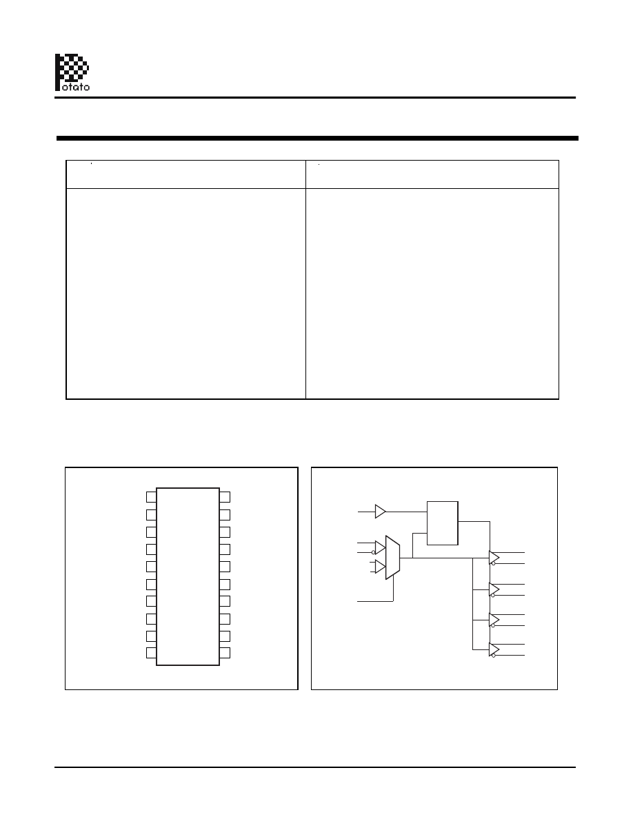
The PO74HSTL85331A is a low skew, high performance
1-to-4 Crystal Oscillator/Differential-to-3.3V HSTL
fanout buffer of High Performance Clock Solutions from
PotatoSemi. The PO74HSTL85331A has selectable
differential clock or crystal inputs. The CLK, nCLK pair
can accept most standard differential input levels. The
clock enable is internally synchronized to eliminate runt
pulses on the outputs during asynchronous
assertion/deassertion of the clock enable pin.
Guaranteed output and part-to-part skew characteristics
make the PO74HSTL85331A ideal for those applications
demanding well defined performance and repeatability.
FEATURES:
Pin Configuration
Logic Block Diagram
DESCRIPTION:
CL
CLKIN / XTAL1
K
nCLK
CLKOUT / XTAL2
Q0
nQ0
Q1
nQ1
Q2
nQ2
Q3
nQ3
0
1
CLK_EN
CLK_SEL
D
Q
LE
GND
CLK_EN
CLK_SEL
CLK
nCLK
XTAL1
XTAL2
nc
nc
V
CC
1
2
3
4
5
6
7
8
9
10
20
19
18
17
16
15
14
13
12
11
Q0
nQ0
V
CC
Q1
nQ1
Q2
nQ2
V
CC
Q3
nQ3
2.3V-3.6V 1:4 Crystal Oscillator/Differential Clock or Data Fanout Buffer
1
01/01/10
Potato Semiconductor Corporation
PO74HSTL85331A
www.potatosemi.com
700MHz TTL/CMOS Potato Chip
. 5000V Human-BodyModel (A114-A)
. 200V MachineModel (A115-A)
Function Table
Pin Characteristics
Pin Definitions
l
o
b
m
y
S
r
e
t
e
m
a
r
a
s
P
n
o
i
ti
d
n
o
C
t
s
e
m
T
u
m
i
n
i
M
l
a
c
i
p
y
T
m
u
m
i
x
a
M
s
ti
n
U
C
N
I
e
c
n
a
ti
c
a
p
a
C
t
u
p
n
I
F
4
p
R
P
U
L
L
U
P
r
o
t
s
i
s
e
R
p
u
ll
u
P
t
u
p
n
I
88
88
K
K
R
N
W
O
D
L
L
U
P
r
o
t
s
i
s
e
R
n
w
o
d
ll
u
P
t
u
p
n
I
s
t
u
p
n
s
I
t
u
p
t
u
O
N
E
_
K
L
L
C
E
S
_
K
L
e
C
c
r
u
o
S
d
e
t
c
e
l
e
3
S
Q
:
0
3
Q
Q
n
:
0
Q
n
K
0
0
L
C
n
,
K
L
W
C
O
L
;
d
e
l
b
a
s
i
H
D
G
I
H
;
d
e
l
b
a
s
i
D
2
1
0
L
A
T
X
,
1
L
A
T
W
X
O
L
;
d
e
l
b
a
s
i
H
D
G
I
H
;
d
e
l
b
a
s
i
D
K
0
1
L
C
n
,
K
L
d
C
e
l
b
a
n
d
E
e
l
b
a
n
E
2
1
1
L
A
T
X
,
1
L
A
T
d
X
e
l
b
a
n
d
E
e
l
b
a
n
E
r
o
k
c
o
l
c
t
u
p
n
i
g
n
il
l
a
f
d
n
a
g
n
i
s
i
r
a
g
n
i
w
o
l
o
f
d
e
l
b
a
n
e
r
o
d
e
l
b
a
s
i
d
e
r
a
s
t
u
p
t
u
o
k
c
o
l
c
e
h
t
,
s
e
h
c
ti
w
s
N
E
_
K
L
C
r
e
tf
A
n
i
n
w
o
h
s
s
a
e
g
d
e
r
o
t
a
ll
i
c
s
o
l
a
t
s
y
r
c
1
e
r
u
g
i
F
.
d
e
b
i
r
c
s
e
d
s
a
s
t
u
p
n
i
2
L
A
T
X
,
1
L
A
T
X
d
n
a
K
L
C
n
,
K
L
C
e
h
t
f
o
n
o
it
c
n
u
f
a
e
r
a
s
t
u
p
t
u
o
e
h
t
f
o
e
t
a
t
s
e
h
t
,
e
d
o
m
e
v
it
c
a
e
h
t
n
I
.
B
3
e
l
b
a
T
n
i
r
e
b
m
u
N
e
m
a
N
e
p
y
n
T
o
i
t
p
i
r
c
s
e
D
1
V
E
E
r
e
w
o
P
2
N
E
_
K
L
C
t
u
p
n
I
p
u
ll
u
P
.t
u
p
n
i
k
c
o
l
c
s
w
o
ll
o
f
s
t
u
p
t
u
o
k
c
o
l
c
,
H
G
I
H
n
e
h
W
.
e
l
b
a
n
e
k
c
o
l
c
g
n
i
z
i
n
o
r
h
c
n
y
S
.
h
g
i
h
d
e
c
r
o
f
e
r
a
s
t
u
p
t
u
o
Q
n
,
w
o
l
d
e
c
r
o
f
e
r
a
s
t
u
p
t
u
o
Q
,
W
O
L
n
e
h
W
.
s
l
e
v
e
l
e
c
a
f
r
e
t
n
i
L
T
T
V
L
/
S
O
M
C
V
L
3
L
E
S
_
K
L
C
t
u
p
n
I
n
w
o
d
ll
u
P
.t
u
p
n
i
K
L
C
n
,
K
L
C
s
t
c
e
l
e
s
,
W
O
L
n
e
h
W
.t
u
p
n
i
t
c
e
l
e
s
k
c
o
l
C
.
s
l
e
v
e
l
e
c
a
f
r
e
t
n
i
L
T
T
V
L
/
S
O
M
C
V
L
.t
u
p
n
i
L
A
T
X
s
t
c
e
l
e
s
,
H
G
I
H
n
e
h
W
4
K
L
C
t
u
p
n
I
n
w
o
d
ll
u
.
P
t
u
p
n
i
k
c
o
l
c
l
a
it
n
e
r
e
f
fi
d
g
n
it
r
e
v
n
i
-
n
o
N
5
K
L
C
n
t
u
p
n
I
p
u
ll
u
.
P
t
u
p
n
i
k
c
o
l
c
l
a
it
n
e
r
e
f
fi
d
g
n
it
r
e
v
n
I
6
1
L
A
T
X
t
u
p
n
I
n
w
o
d
ll
u
.
P
t
u
p
n
i
r
o
t
a
ll
i
c
s
o
l
a
t
s
y
r
C
7
2
L
A
T
X
t
u
p
n
I
p
u
ll
u
.
P
t
u
p
n
i
r
o
t
a
ll
i
c
s
o
l
a
t
s
y
r
C
9
,
8
c
n
d
e
s
u
n
.
U
t
c
e
n
n
o
c
o
N
8
1
,
3
1
,
0
1
V
C
C
r
e
w
o
.
P
s
n
i
p
y
l
p
p
u
s
e
v
it
i
s
o
P
2
1
,
1
1
3
Q
,
3
Q
n
t
u
p
t
u
.
O
s
l
e
v
e
l
e
c
a
f
r
e
t
n
i
.
s
t
u
p
t
u
o
k
c
o
l
c
l
a
it
n
e
r
e
f
fi
D
5
1
,
4
1
2
Q
,
2
Q
n
t
u
p
t
u
.
O
s
l
e
v
e
l
e
c
a
f
r
e
t
n
i
.
s
t
u
p
t
u
o
k
c
o
l
c
l
a
it
n
e
r
e
f
fi
D
7
1
,
6
1
1
Q
,
1
Q
n
t
u
p
t
u
.
O
s
l
e
v
e
l
e
c
a
f
r
e
t
n
i
.
s
t
u
p
t
u
o
k
c
o
l
c
l
a
it
n
e
r
e
f
fi
D
0
2
,
9
1
0
Q
,
0
Q
n
t
u
p
t
u
.
O
s
l
e
v
e
l
e
c
a
f
r
e
t
n
i
.
s
t
u
p
t
u
o
k
c
o
l
c
l
a
it
n
e
r
e
f
fi
D
:
E
T
O
N
p
u
ll
u
P
d
n
a
n
w
o
d
ll
u
P
.
s
e
u
l
a
v
l
a
c
i
p
y
t
r
o
f
,
s
c
it
s
i
r
e
t
c
a
r
a
h
c
n
i
P
,
2
e
l
b
a
T
e
e
S
.
s
r
o
t
s
i
s
e
r
t
u
p
n
i
l
a
n
r
e
t
n
i
o
t
r
e
f
e
r
GND Pin
HSTL
HSTL
HSTL
HSTL
2.3V-3.6V 1:4 Crystal Oscillator/Differential Clock or Data Fanout Buffer
2
01/01/10
Potato Semiconductor Corporation
PO74HSTL85331A
www.potatosemi.com
700MHz TTL/CMOS Potato Chip
DC Electrical Characteristics
Symbol
Description
Test Conditions
Min
Typ
Max
Unit
V
OH
Output High voltage
Vcc=3V Vin=V
IH
or V
IL
, I
OH
= -12mA
2.4
3
-
V
V
OL
Output Low voltage
Vcc=3V Vin=V
IH
or V
IL
, I
OH
=12mA
-
0.3
0.5
V
V
IK
Clamp diode voltage
Vcc = Min. And
I
IN
= -18mA
-
-0.7
-1.2
V
Notes:
1. For conditions shown as Max. or Min., use appropriate value specified under Electrical Characteristics for the applicable device type.
2.
Typical values are at Vcc = 3.3V, 25
°
C ambient.
3.
This parameter is guaranteed but not tested.
4.
Not more than one output should be shorted at one time. Duration of the test should not exceed one second.
5.
VoH = Vcc – 0.6V at rated current
Maximum Ratings
Description
Max
Unit
Storage Temperature
-65 to 150
°
C
Operation Temperature
-40 to 85
°
C
Operation Voltage
-0.5 to +4.6
V
Input Voltage
-0.5 to +5.5
V
Output Voltage
-0.5 to Vcc+0.5
V
Note:
stresses greater than listed under
Maximum
Ratings
may
cause
permanent damage to the device. This
is a stress rating only and functional
operation of the device at these or any
other conditions above those indicated
in the operational sections of this
specification is not implied. Exposure
to absolute maximum rating conditions
for extended periods may affect
reliability specification is not implied.
Multiple Supplies: The Voltage on any input or I/O pin cannot exceed the power pin during power-up. Power supply sequencing is NOT required.
2.3V-3.6V 1:4 Crystal Oscillator/Differential Clock or Data Fanout Buffer
3
01/01/10
Potato Semiconductor Corporation
PO74HSTL85331A
www.potatosemi.com
700MHz TTL/CMOS Potato Chip
Power Supply Characteristics
Symbol
Description
Test Conditions (1)
Min
Typ
Max
Unit
Icc
Q
Quiescent Power Supply Current
Vcc=Max, Vin=Vcc or GND
-
0.1
30
uA
Notes:
Notes:
1. For conditions shown as Max. or Min., use appropriate value specified under Electrical Characteristics for the applicable device type.
2. Typical values are at Vcc = 3.3V, 25
°
C ambient.
3. This parameter is guaranteed but not tested.
4. Not more than one output should be shorted at one time. Duration of the test should not exceed one second.
Switching Characteristics
t
i
n
U
x
a
M
)
1
(
s
n
o
i
t
i
d
n
o
C
t
s
e
T
n
o
i
t
p
i
r
c
s
e
D
l
o
b
m
y
S
t
PD
Propagation Delay CLK to Output pair
CL = 15pF
3.7
ns
tr/tf
Rise/Fall Time
0.8V – 2.0V
0.8
ns
tsk(o)
Output Pin to Pin Skew (Same Package)
ps
ps
tsk(pp)
Output Skew (Different Package)
fmax
F
p
5
1
=
L
C
y
c
n
e
u
q
e
r
F
t
u
p
n
I
250
MHz
fmax
F
p
5
=
L
C
y
c
n
e
u
q
e
r
F
t
u
p
n
I
300
MHz
fmax
F
p
2
=
L
C
y
c
n
e
u
q
e
r
F
t
u
p
n
I
400
MHz
Notes:
1. See test circuits and waveforms.
See schematic example.
2. tpLH, tpHL, tsk(p), and tsk(o) are production tested. All other parameters guaranteed but not production tested.
3. Airflow of 1m/s is recommended for frequencies above 133MHz
CL = 15pF, 125MHz
CL = 15pF, 125MHz
50
300
400
570
700
Crystal Oscillator Test Conditions
s
n
o
i
ti
d
n
o
C
t
s
Output Frequency
50
3.579
14.318
28
250
400
462
e
T
ts
i
n
U
MHz
MHz
MHz
X1=50MHz, C4=50pf, C5=50pf, R1=3K
X1=3.579MHz, C4=100pf, C5=100pf
X1=14.318MHz, C4=50pf, C5=50pf
X1=28MHz, C4=50pf, C5=50pf, R1=5.1K
X1=250MHz, C4=0, C5=0, R1=1K
X1=400MHz, C4=0, C5=0, R1=1K
X1=462MHz, C4=0, C5=0, R1=1K
MHz
MHz
MHz
MHz
2.3V-3.6V 1:4 Crystal Oscillator/Differential Clock or Data Fanout Buffer
4
01/01/10
Potato Semiconductor Corporation
PO74HSTL85331A
www.potatosemi.com
700MHz TTL/CMOS Potato Chip
Test Waveforms
VPP RANGE
0V-VCC
FIGURE 1. LVDS/ PECL/ ECL/ HSTL /DIFFERENTIAL INPUT WAVEFORM DEFINITIONS
FIGURE 2. HSTL/HSTL OUTPUT
FIGURE 3. Propogation Delay, Output pulse skew, and output-to-output skew
for both CLKA or CLKB to output pair
FIGURE 4. CLK_EN Timing Diagram
VPP
TPHL
TPLH
TPD
INPUT
CLOCK
OUTPUT
CLOCK
ANOTHER
OUTPUT
CLOCK
VO
tSK(O)
VCC= 3.3V
VEE=0.0V
VIH
VIL
VPP
VCC
VEE
VO
tr,tf,
20-80%
Enabled
Disabled
nCLK
CLK
CLK_EN
nQ0:nQ3
Q0:Q3
2.3V-3.6V 1:4 Crystal Oscillator/Differential Clock or Data Fanout Buffer
5
01/01/10
Potato Semiconductor Corporation
PO74HSTL85331A
www.potatosemi.com
700MHz TTL/CMOS Potato Chip
Test Circuit
50Ohm
50Ohm
50pF
to
2pF
50pF
to
2pF
Schematic Example
X1
C3
0.1u
U1
1
2
3
4
5
6
7
8
9
10
11
12
13
14
15
16
20
19
18
17
VEE
CLK_EN
CLK_SEL
CLK
nCLK
XTAL1
XTAL2
NC
NC
VCC
nQ3
Q3
VCC
nQ2
Q2
nQ1
Q0
nQ0
VCC
Q1
3.3V
R12
1K
3.3V
3.3V
C2
0.1u
+
-
+
-
+
-
+
-
3.3V
R11
1K
R1
C4
40p - 60pF
C1
0.1u
C5
SPARE
3.3V
2.3V-3.6V 1:4 Crystal Oscillator/Differential Clock or Data Fanout Buffer
6
01/01/10
Potato Semiconductor Corporation
PO74HSTL85331A
www.potatosemi.com
700MHz TTL/CMOS Potato Chip
2.3V-3.6V 1:4 Crystal Oscillator/Differential Clock or Data Fanout Buffer
Packaging Mechanical Drawing: 20 pin TSSOP
.252
.260
.047
1.20
.002
.006
SEATING
PLANE
.0256
BSC
1
20
.169
.177
0.05
0.15
4.3
4.5
6.4
6.6
0.65
0.19
0.30
.007
.012
Max
.018
.030
.004
.008
.238
.269
6.1
6.7
0.45
0.75
0.09
0.20
X.XX
X.XX
DENOTES DIMENSIONS
IN MILLIMETERS
IC Ordering Information
Top-Marking
Ordering Code
Package
Pb-free & Green
PO74HSTL85331ASU for Tube
PO74HSTL85331ASR for Tape & Reel
PO74HSTL85331AS
-40
°
C to 85
°
C
-40
°
C to 85
°
C
TA
Pb-free & Green
20pin 173mil TSSOP
IC Package Information
PACKAGE
T
16
8
Top Left Corner
39 (12”)
3000
64 (20”)
74
20pin 173mil TSSOP
CODE
PACKAGE
TYPE
TAPE
WIDTH
TAPE TRAILER
TUBE
TAPE & REEL
LENGTH
TAPE
PITCH
QTY
LENGTH
TAPE LEADER
PER TAPE
QTY
PER
PIN 1 LOCATION
(mm)
(mm)
7
01/01/10
Potato Semiconductor Corporation
PO74HSTL85331A
www.potatosemi.com
700MHz TTL/CMOS Potato Chip
PO74HSTL85331AS
20pin 173mil TSSOP