PR
O
DU
CT S
EL
EC
TIO
N G
UID
E
20
18
PRODUCT SELECTION GUIDE
2018
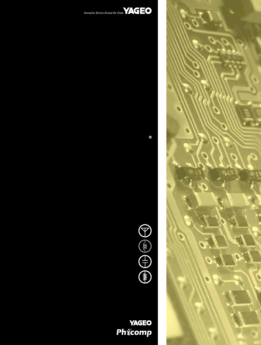
SMD RESISTORS + MLCC
SMD CERAMIC EMI FILTER CAPACITORS - X2Y
®
WIRELESS COMPONENTS
MULTILAYER CHIP VARISTORS
www
.yageo.com
Date of release: Dec. 2017
Printed in Taiwan
Document order number
: YL 100 00164
© YAGEO Corporation
All rights are reserved. Reproduction in whole or in part is prohibited without the prior written consent of the copyright owner.
The information presented in this document does not form part of any quotation or contract, is believed to be accurate and reliable and may be changed without notice.
No liability will be accepted by the publisher for any consequence of its use. Publication thereof does not convey nor imply any license under patent or other industrial or intellectual property rights.
For a complete listing of all Yageo sales offi ces, distributors, and representatives, please visit "contact us" at
www.yageo.com
YAGEO - A GLOBAL COMPANY
ASIA
HQ
Taipei, Taiwan
Tel. +886 2 6629 9999
Fax. +886 2 6628 8886
Kuala Lumpur, Malaysia
Tel. +60 3 8063 8864
Fax. +60 3 8063 7376
Penang, Malaysia
Tel. +60 4 3973049
Fax. +60 4 3973050
EUROPE
Munich, Germany
Tel. +49 8990 7784 380
Fax. +49 8990 7784 379
Milan, Italy
Tel. +39 02 6129 1017
Fax. +39 02 6601 7490
Roermond, Benelux
Tel. +31 475 385 555
Fax. +31 475 385 589
Szombathely, Hungary
Tel. +36 94 517 702
Fax. +36 94 517 701
Moscow, Russian Federation
Tel. +7 965 408 18 11
Fax. +7 498 610 07 07
NORTH AMERICA
San Jose, U.S.A.
Tel. +1 408 240 6200
Fax. +1 408 240 6201
Mexico
Tel. +52 33 31330631
Fax. +1 408 240 6201
Suzhou, China
Tel. +86 512 6825 5568
Fax. +86 512 6825 5386
Shanghai, China
Tel. +86 21 64858697
Dongguan, China
Tel. +86 769 8772 0275
Fax. +86 769 8791 0053
Tokyo, Japan
Tel. +81 3 6809 3972
Fax. +81 3 6809 3982
Seongnam, Korea
Tel. +82 31 712 4797
Fax. +82 31 712 5866
Singapore
Tel. +65 6244 7800
Fax. +65 6244 4943