
Pulse Antenna Solutions
Basics of Pulse Ceramic Chip Antenna
Pulse | 2015
Pulse Antenna Solutions
Basics of Pulse Ceramic Chip Antenna
Pulse | 2015

2
CONFIDENTIAL AND PROPRIETARY
Pulse Electronics, Inc.
All Rights Reserved.
No Copying or Reproduction Allowed
Topics
• Antenna Design Method
• PIFA Antenna Basics
• Considerations of Antenna Implementation
on PCB

3
CONFIDENTIAL AND PROPRIETARY
Pulse Electronics, Inc.
All Rights Reserved.
No Copying or Reproduction Allowed
Antenna Design Method
4
CONFIDENTIAL AND PROPRIETARY
Pulse Electronics, Inc.
All Rights Reserved.
No Copying or Reproduction Allowed
Simulation / Design Tools
• Mechanical Design:
o
Catia, I-DEAS, PRO-E, SolidWorks
o
Electrical Design:
o
CST MWS, IE3D, AWR Aplac, AWR MWO,
Ensemble, HFSS Ansoft Designer
Structural Simulation
Tolerance Analysis
Material Studies
5
CONFIDENTIAL AND PROPRIETARY
Pulse Electronics, Inc.
All Rights Reserved.
No Copying or Reproduction Allowed
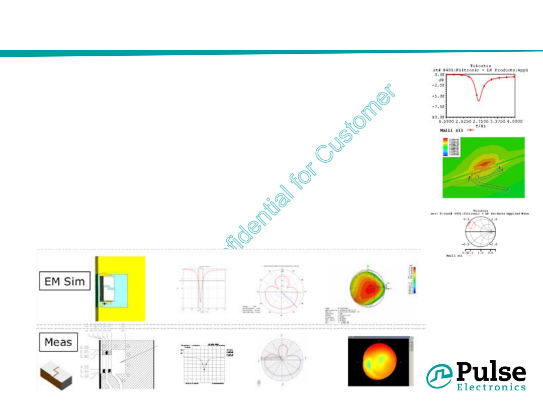
Example of EM simulation model
• W3008 model build using CST MWS
6
CONFIDENTIAL AND PROPRIETARY
Pulse Electronics, Inc.
All Rights Reserved.
No Copying or Reproduction Allowed
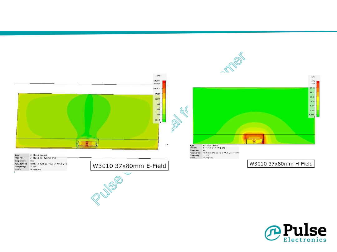
Simulated EM fields (Example: W3010)
Whole PCB is “hot”
7
CONFIDENTIAL AND PROPRIETARY
Pulse Electronics, Inc.
All Rights Reserved.
No Copying or Reproduction Allowed
PIFA Antenna Theory
(Ceramic PIFA)
8
CONFIDENTIAL AND PROPRIETARY
Pulse Electronics, Inc.
All Rights Reserved.
No Copying or Reproduction Allowed
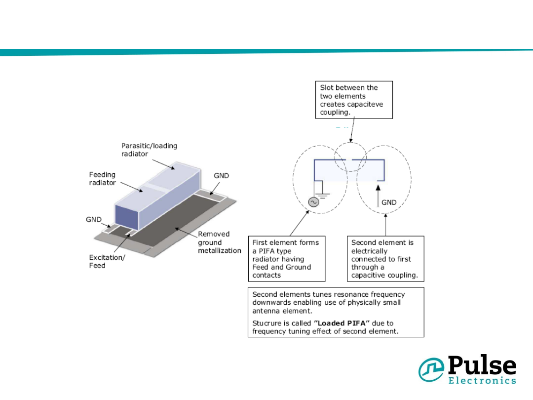
Loaded PIFA Structure
9
CONFIDENTIAL AND PROPRIETARY
Pulse Electronics, Inc.
All Rights Reserved.
No Copying or Reproduction Allowed
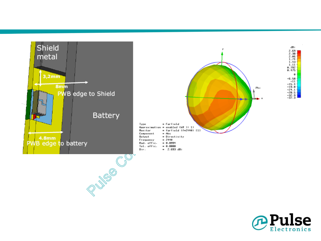
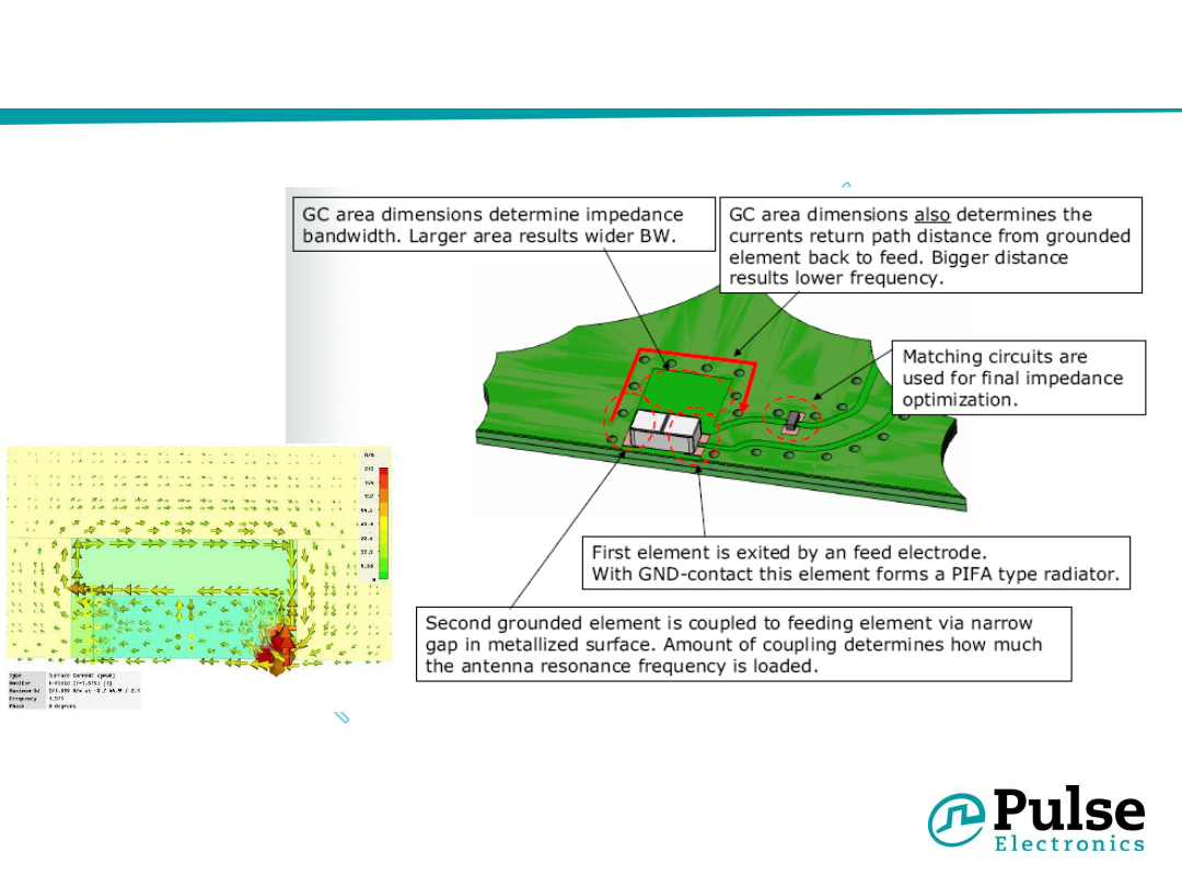
Function of Ground Clearance area / layout
Simulated Surface currents
(Example: W3010)
10
CONFIDENTIAL AND PROPRIETARY
Pulse Electronics, Inc.
All Rights Reserved.
No Copying or Reproduction Allowed
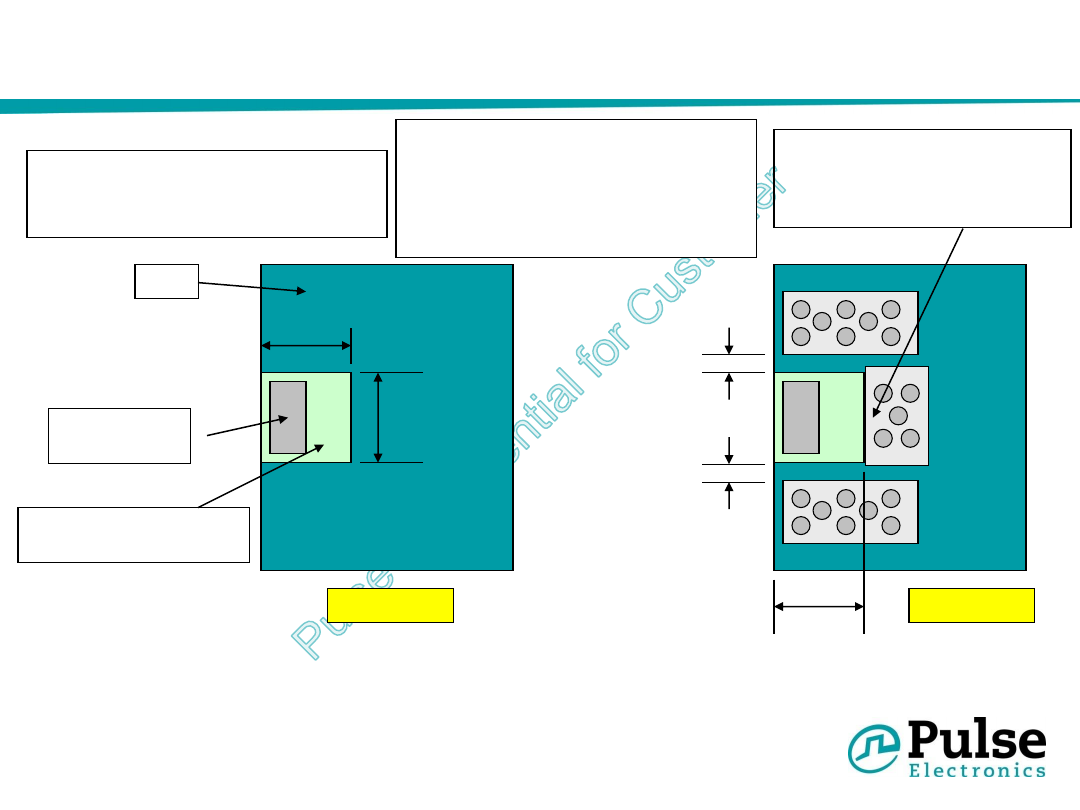
Why three pads on board and two on antenna?
• Basic antenna is PIFA type; Feed and GND are
needed for first electrode
• Antenna pad short circuits the two pads on board
• Board pads are normally kept separate to make
impedance matching more stable and straight forward

11
CONFIDENTIAL AND PROPRIETARY
Pulse Electronics, Inc.
All Rights Reserved.
No Copying or Reproduction Allowed
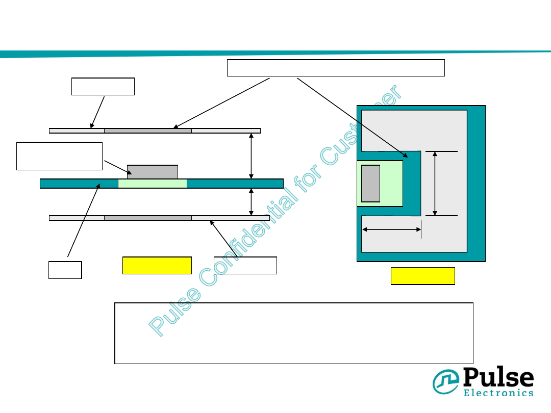
Benefits of “Loaded PIFA”
• Can achieve extremely good efficiency number when properly
implemented, 90%
• Creates close to omni-directional 3D radiation pattern
– Above mentioned features are due to combination of ceramic
antenna element and board resonance radiation
• High immunity of frequency detuning due to user tissue (body, hand,
head) and surrounding mechanics

12
CONFIDENTIAL AND PROPRIETARY
Pulse Electronics, Inc.
All Rights Reserved.
No Copying or Reproduction Allowed
Considerations of Antenna
Implementation on PCB

13
CONFIDENTIAL AND PROPRIETARY
Pulse Electronics, Inc.
All Rights Reserved.
No Copying or Reproduction Allowed
PCB effects
• Loaded PIFA antenna is short circuited to PCB ground
• Antenna element electrical length is λ/4
• PCB has major effect in overall antenna performance
figures!
– PCB electrical length (examples shown later in this
presentation)
– Antenna position on board (examples shown later in
this presentation)
– Grounding points on antenna layout
– PCB layout and size affects on antenna:
• Frequency
• Bandwidth
• Feed impedance
• Total radiation performance
14
CONFIDENTIAL AND PROPRIETARY
Pulse Electronics, Inc.
All Rights Reserved.
No Copying or Reproduction Allowed
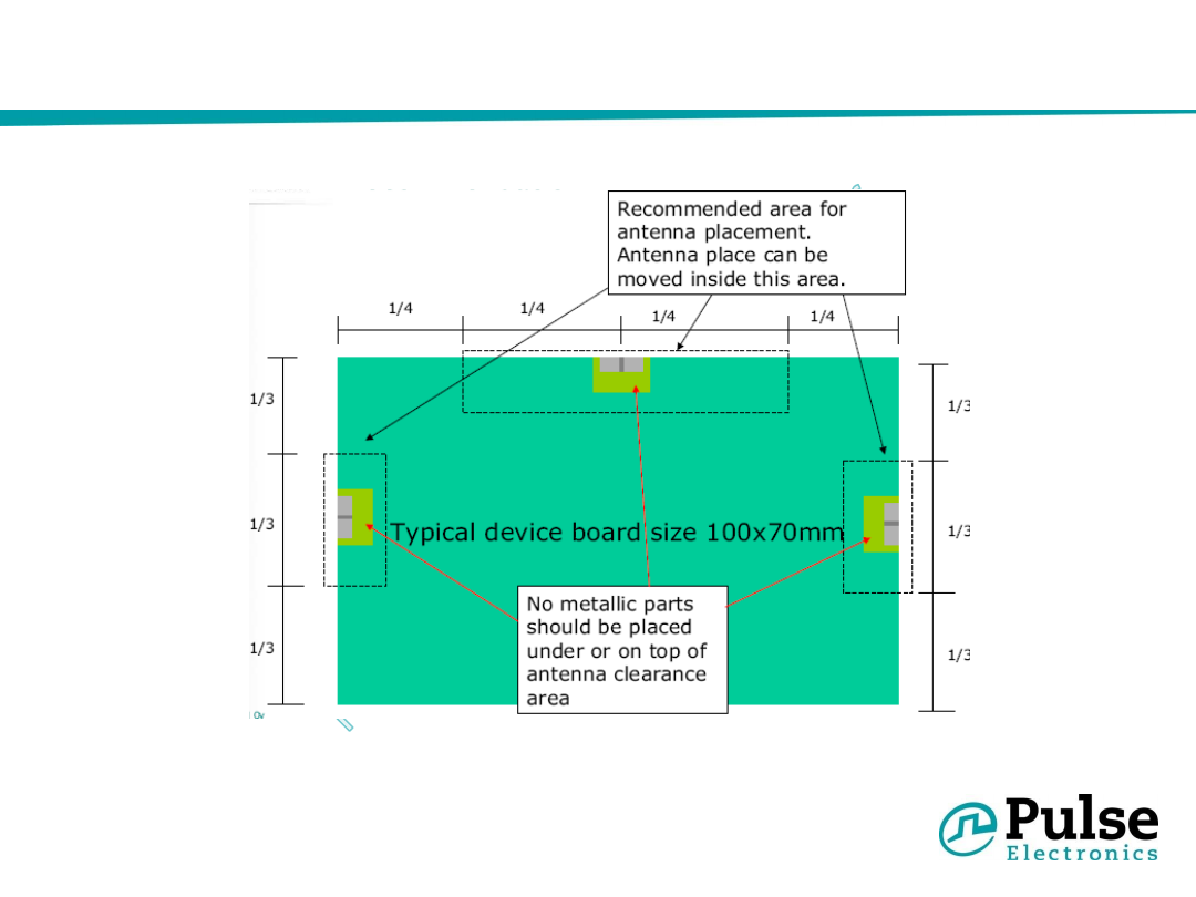
Antenna Placement Recommendations
• Fractions represent wavelengths
15
CONFIDENTIAL AND PROPRIETARY
Pulse Electronics, Inc.
All Rights Reserved.
No Copying or Reproduction Allowed
Recommended metal object guard distances for ground clearance
(Example: PIFA type W3010 chip antenna)
2mm clearance
2mm clearance
6.25mm
Metal objects like shield cans
can be placed on the edge of
the antenna ground clearance
area
ANTENNA
10x3.2x2mm
Ground Clearance area
10.6x6.25mm
PWB
10.6mm
6.25mm
Same design rules apply to
both sides of the PWB, top and
bottom
TOP VIEW
Height of metal object has
effect on antenna performance.
Over 2mm heigh metallic parts
decrade antenna performance if
placed close to antenna.
TOP VIEW
•
Include metallic objects close to antenna into your mock up
testing as early as possible!
•
Common Metallic objects : Connector, Switches, Wibra,
Microphone, Shield cans, Etc.
16
CONFIDENTIAL AND PROPRIETARY
Pulse Electronics, Inc.
All Rights Reserved.
No Copying or Reproduction Allowed
Recommended metal object guard distances for ground clearance
(Example: PIFA type W3011 chip antenna)
SIDE VIEW
TOP VIEW
PWB
ANTENNA
3.2x1.6x1.1mm
9x7mm metal free area around the antenna
9mm
7mm
Metal plate
Metal plate
Distance from PWB
6.0mm
Distance from PWB
5.0mm
This information of metallic plate/cover guard distance is indicative only
and should be concidered as minimum keep out distances. The best
radiating performance is allways achieved when antenna is in as ”free
space” condition as possible. It is recommended to use low dielelctric low
loss plastic covers.

17
CONFIDENTIAL AND PROPRIETARY
Pulse Electronics, Inc.
All Rights Reserved.
No Copying or Reproduction Allowed
Recommended metal object guard distances for ground clearance
(Example: PIFA type W3010 chip antenna)
SIDE VIEW
TOP VIEW
PWB
ANTENNA
10x3.2x2mm
15x8mm metal free area around the antenna
15mm
8mm
Metal plate
Metal plate
Distance from PWB
6.0mm
Distance from PWB
5.0mm
This information of metallic plate/cover guard distance is indicative only
and should be concidered as minimum keep out distances. The best
radiating performance is allways achieved when antenna is in as ”free
space” condition as possible. It is recommended to use low dielelctric low
loss plastic covers.
18
CONFIDENTIAL AND PROPRIETARY
Pulse Electronics, Inc.
All Rights Reserved.
No Copying or Reproduction Allowed
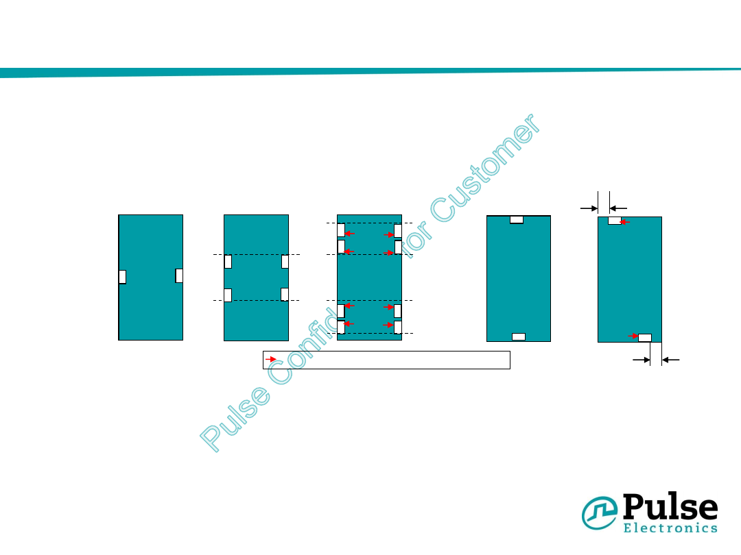
“OK to use” antenna position on PWB
(Example: W3010 GPS)
•
Typical board side 35..45 x 35..110mm
•
Each used position may require external matching components and
ground clearance area modifications for finetuning the impedance
matching and center frequency tuning
Left or right
side center:
Best position
Midle third of the
PWB:
Ok position
without significant
change in
performance
Minimum 5 to
10mm from top or
bottom edge:
Position with about
0.5..1dB drop in
performance
Min 5..10mm
Min 5..10mm
Top or bottom end
of PWB:
Position with about
0.5 to 1dB drop in
performance,
depends on bord
width, wider is
better
1.
2.
3.
4.
PREFERRED FEED ORIENTATION, No impact if not mentioned
5.
Min 7..10mm
Top or bottom end
corner of PWB:
Position with about
0.5 to 1dB drop in
performance,
depends on bord
width, wider is
better
19
CONFIDENTIAL AND PROPRIETARY
Pulse Electronics, Inc.
All Rights Reserved.
No Copying or Reproduction Allowed
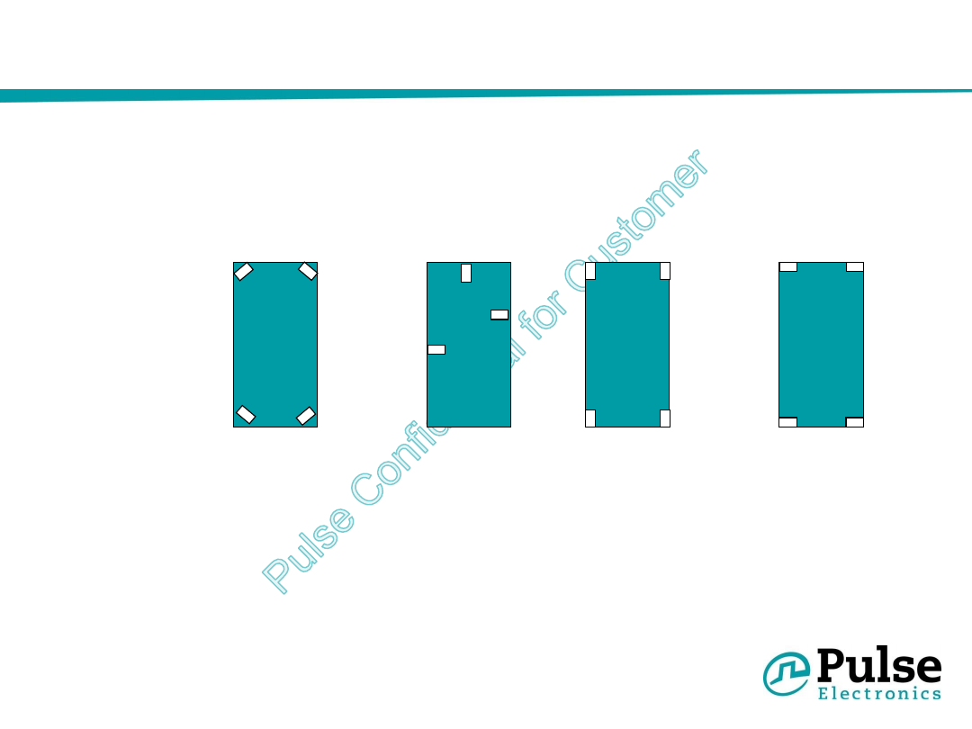
“
NOT OK
to use” antenna position on PWB
(Example: W3010 GPS)
•
Below mentioned positions will result to poor performance of the
antenna
Top or bottom
corner 45deg
angle:
NOT to use
”Sideways” in
any position:
NOT to use
6.
7.
Directly on
corner
vertically:
NOT to use
Directly on
corner
horizontally:
NOT to use
8.
9.

20
CONFIDENTIAL AND PROPRIETARY
Pulse Electronics, Inc.
All Rights Reserved.
No Copying or Reproduction Allowed
Do’s and Dont’s
•
Do
– Use Pulse footprint recommendation as baseline
– Place enough grounding vias on the edges of the clearance area. Route vias
through all layers in the board.
– Clear the metal away from all the layers of the board
– Make needed matching and tuning by clearance area changes and external
mathing components
– Use plastic covers
•
Do
NOT
– Place antenna directly in the corner of the board
– Place any components or traces on the antenna clearance area (all layers)
– Place metallic covers on top or below the antenna and clearance area
21
CONFIDENTIAL AND PROPRIETARY
Pulse Electronics, Inc.
All Rights Reserved.
No Copying or Reproduction Allowed
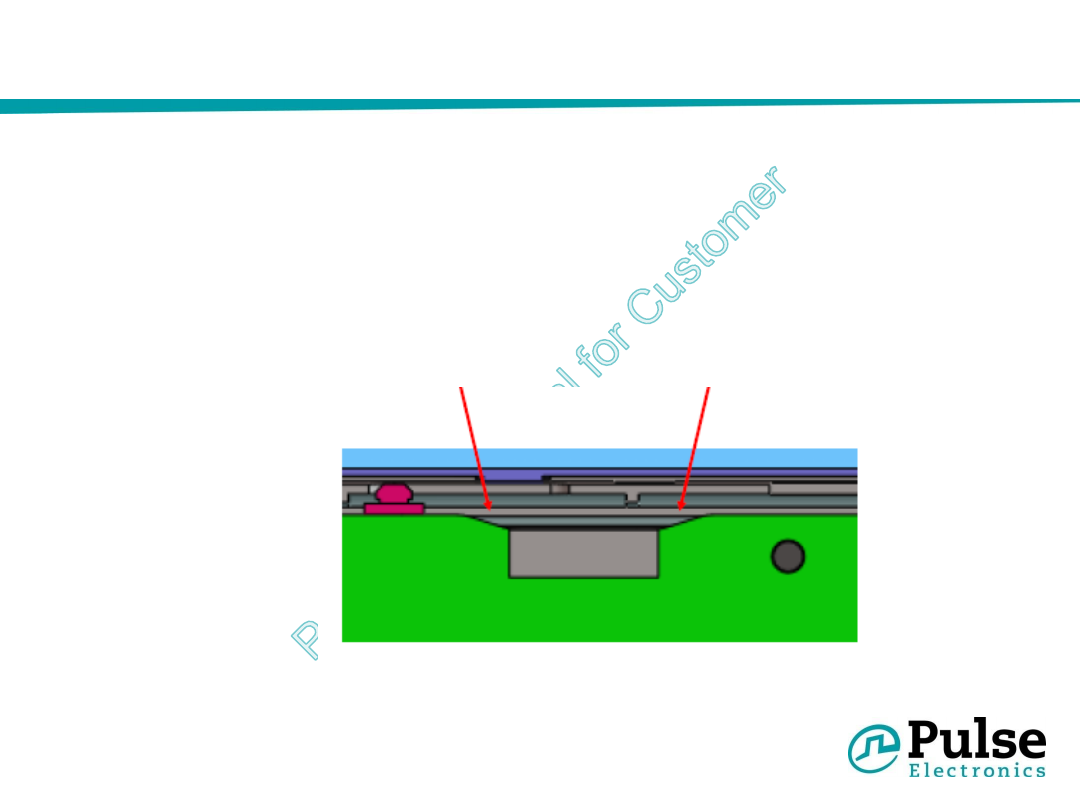
Board edge
• It is ok to have antenna moved couple millimeters
inwards to PCB
• Ground copper on antenna corners should be chamfered
to minimize effect on performance
22
CONFIDENTIAL AND PROPRIETARY
Pulse Electronics, Inc.
All Rights Reserved.
No Copying or Reproduction Allowed
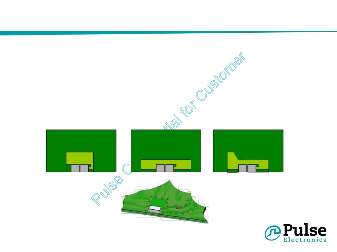
Ground Clearance area shape
• GC-area does not need to be square shaped. Square shape is
presented in Pulse apps notes as a standard starting point for the
layout work.
• Arbitrary form GC-areas can be used as long as total area and
current return path distance is optimized to give correct resonant
frequency and BW

23
CONFIDENTIAL AND PROPRIETARY
Pulse Electronics, Inc.
All Rights Reserved.
No Copying or Reproduction Allowed
Consistency of Ground
• Antenna sees the whole PCB as ground plane
• Overall board dimensions determine the PCB electrical
length
• Especially around the GC area ground pour needs to be
solid
• Ground pour does not need to be continued on same
layer over the whole board. Several layers can be
connected together with via holes

24
CONFIDENTIAL AND PROPRIETARY
Pulse Electronics, Inc.
All Rights Reserved.
No Copying or Reproduction Allowed
Multi-layer board considerations
• Again most critical point on multi-layer layout is the GC
area surroundings
• All layers around the GC area must be connected
together to avoid signal coupling/leaking into gaps
between the layers
• Poorly grounded GC are also causes problems in
impedance matching and frequency control
• DC voltage layers can be left floating as long as metal of
that layer does not overlap with the GC area

25
CONFIDENTIAL AND PROPRIETARY
Pulse Electronics, Inc.
All Rights Reserved.
No Copying or Reproduction Allowed
“THANK YOU”