Spansion
®
Product Selector Guide
January 2014
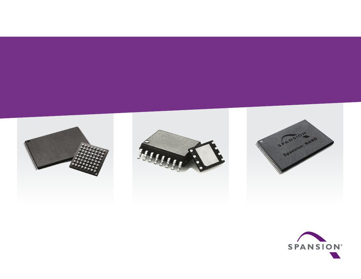
Parallel NOR
Flash
Serial NOR
Flash
SLC NAND
Flash