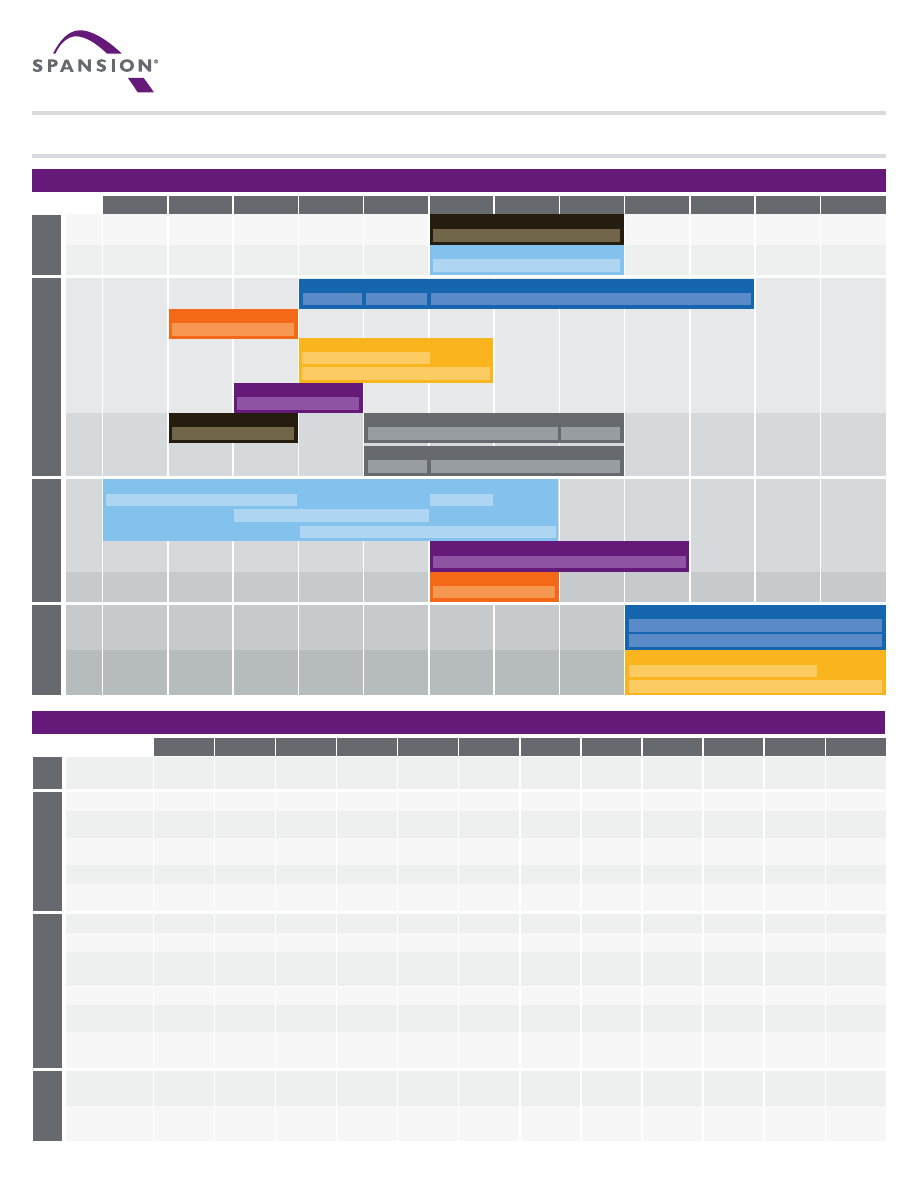
Hyper
Flash
S26KL128S
S26KS128S
S26KL256S
S26KS256S
S26KL512S
S26KS512S
24-BALL BGA
S29GL032N
S25FL123K
S70GL02GS
S29GL064S
S29AL016J
S29GL256S
S29GL512S
S29GL128S
S29GL01GS
S29GL01GP
S25FL208K
S25FL216K
S25FL116K
S25FL204K
Pa
ra
lle
l N
O
R
Se
ri
al NO
R
NAN
D
S34ML02G1
S34ML02G2
S34ML08G1
S34ML08G2
S34ML08G1
S34MS08G2
S34ML02G1
S34MS02G1
S34ML02G2
S34MS02G2
S25FL208K
S25FL204K
S25FL164K
S25FS128S
S25FL116K
S25FL164K
S25FL032P
S25FL132K
S25FS128S
S25FL127S
S25FL032P
S25FL132K
S25FL064P
S25FL164K
S25FL512S
S25FL116K
S25FL256S
S25FS256S
S25FL128S
S25FL128P
S25FL129P
S25FL127S
S25FL256S
S25FS256S
S25FL064P
S25FL164K
S25FL032P
S25FL512S
S70FL01GS
S25FL256S
S25FS256S
S25FL128S
S25FL128P
S25FL129P
S25FL032P
S25FL064P
S25FL128S
S25FS128S
S25FL127S
S25FL129P
S34ML04G1
S34ML04G2
S34MS04G1
S34MS04G2
S29GL032N
S29JL032J
S29AL008J
S29AS008J
S29AL016J
S29AS016J
S29GL064S
S29JL064J
S29GL032N
S29GL064S
S29GL512S
S29GL512P
S29GL128S
S29GL128P
S29PL127J
S29GL256S
S29GL256P
S29AL008J
S29AS008J
S29AL016J
S29AS016J
S29GL032N
S29JL032J
S29PL032J
S29GL064S
S29JL064J
S29PL064J
S29GL128S
S29GL128P
S29GL256S
S29GL256P
S29GL512S
S29GL512P
S29GL01GS
S29GL01GP
S25FL032P
S25FL132K
S25FL216K
S25FL116K
S34ML01G1
S34ML01G2
S34ML01G1
S34ML01G2
S34MS01G1
S34MS01G2
S34ML04G1
S34ML04G2
S34MS04G1
S34MS04G2
48-PIN TSOP
56-PIN TSOP
64-BALL
FORTIFIED BGA
(1.0 MM PITCH)
8-PIN SO
(150 MIL)
8-PIN SO
(208 MIL)
48-PIN TSOP
63-BALL BGA
8-CONTACT
WSON (6x5 MM)
24-BALL BGA
48-BALL FBGA
(0.8 MM PITCH)
56-BALL FBGA
(0.8MM PITCH)
8-CONTACT
WSON (6X8 MM)
16-PIN SO
(300 MIL)
S25FL132K
S70FL01GS
1.8V
3V
3V
Ser
ia
l NO
R
N
A
N
D
High performance MIO w/DDR
FL-S
3V
GL FAMILY: Leading price-performance, page-mode
GL-N
GL-P/S
Standard interface
AL-J
High performance SRW*
JL-J
PL-J
Burst-mode
CD-J/CL-J
Standard interface
AS-J
High performance Burst-mode SRW* – Mux
NS-P
VS/XS-R
High performance Burst-mode SRW* – DeMux
WS-P
WS-R
4Mb
8Mb
16Mb
32Mb
64Mb
128Mb
256Mb
512Mb
1Gb
2Gb
4Gb
8Gb
1.8V
Pa
ral
lel
N
O
R
*
Simultaneous Read while Write.
spansion’s product portfolio
1.8V
ML FAMILY: High Perf. SLC**
ML-1
High performance multi I/O SPI
FL2-K
FL-P
FL1-K
FL127S
High performance MIO /w DDR
FS-S
MS-1
MS FAMILY: High Perf. SLC**
GL-S
ML-2
MS-2
4Mb
8Mb
16Mb
32Mb
64Mb
128Mb
256Mb
512Mb
1Gb
2Gb
4Gb
8Gb
**
Additional NAND offerings in development. Contact Spansion Sales for information.
universal footprint for ultimate flexibility
Spansion
®
Flash Memory Reference Guide
3V
1.8V
ADM DDR Burst
KL-S
ADM DDR Burst
KS-S
Hyper
Flash
™
Spansion:
915 DeGuigne Drive, PO Box 3453, Sunnyvale, CA 94088-3453 USA
+1 (408) 962-2500 | 1 866 SPANSION | www.spansion.com
© 2014 Spansion®, the Spansion logo, MirrorBit®, MirrorBit® Eclipse™ and combinations thereof, are trademarks
and registered trademarks of Spansion LLC in the United States and other countries. Other names used are for
informational purposes only and may be trademarks of their respective owners.
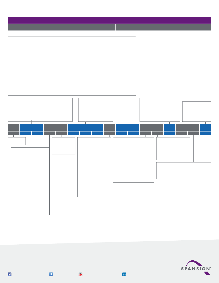
(s) spansion ordering part number construction / single-die products
Generic OPN
Ordering Options
Additional Ordering Options
Prefix
Series
Family
G Density
Tech
Speed /
Bus Width
Package
Temp
Model Number
Pack
type
S
S
1
0
D
H
I
2
9
G
L
0
1
0
G
1
3
Temperature Grade
C = Commercial (0° to +70°C)
W = Wireless (-25° to +85°C)
I = Industrial (-40° to +85°C)
V = In-Cabin (-40° to +105°C)
N = Extended (-40° to +125°C)
29 = Sector Erase NOR Flash memory
34 = Floating Gate NAND
70 = Dual Die Flash Package
Density
001-512 = 1 Mb-512 Mb
204-216 = 4 Mb-16 Mb*
116-164 = 16Mb-64Mb**
127 = 128 Mb***
01G-64G = 1 Gb-64Gb
Packaging Type
0 = Tray
1 = Tube
2 = 7" Tape & Reel
3 = 13" Tape & Reel
Prefix
S = Spansion
Package Type (Family)
Package Material Set
(Varies by Package Type)
A = Leaded
F = Lead (Pb)-Free
H = Low Halogen Lead
(Pb)-Free
Core Volatge
L = 3-volt VCC
D = 2.5-volt VCC
S = 1.8-volt VCC
Process Technology
J = 110nm, Floating Gate
Technology
K = 90nm, Floating Gate
Technology
N = 110nm, MirrorBit
Technology
P = 90nm, MirrorBit
Technology
R = 65nm, MirrorBit
Technology
S = 65nm, MirrorBit
Technology (Eclipse)
1 = NAND Revision 1
(4X nm)
2 = NAND Revision 2
(3X nm)
Flash Interface and
Simultaneous Read-write
Standard
Page
Burst (ADP)
Burst (ADM)
Burst (AADM)
Serial (SPI)
srw
J
P
W
N/V
X
no srw
A
G
F
Speed Option (Parallel NOR and SPI)
Asynchronous (no CLK input)
“Speed Option” represents random access time (ns). If greater than
100ns, use the two leftmost digits.
Synchronous (CLK input)
“Speed Option” represents clock frequency (MHz). First character
represents the data rate, combined with the speed in 100s of MHz:
0
SDR, <100 MHz
A
SDR, 100 MHz
D
DDR, <100 MHz
Second character represents the speed between 0 and 99 MHz:
Bus Width (NAND)
00 = x8 NAND, single die
04 = x16 NAND, single die
01 = x8 NAND, dual die
05 = x16 NAND, dual die
0-4
5-9
10-14
15-19
20-24
25-29
30-34
35-39
40-44
45-49
50-54
55-59
60-64
65-69
70-74
75-79
80-84
85-89
90-94
95-99
100-108
A
B
C
D
E
F
G
H
J
K
L
M
N
P
Q
R
S
T
U
W
X
*
For FL2-K
**
For FL1-K
***
For FL127S
A = BGA-0.5mm pitch
B = BGA-0.8mm pitch (PNOR),
D = Fortified BGA, 9mm x 9mm
F = Fortified BGA, 11mm x 13mm
M = SOIC/SOP
N = SON
Q = PQFP
T = TSOP
Varies for each generic OPN (characters
00-ZZ). Meaning is defined in each
datasheet.
www.facebook.com/spansion twitter: @spansion www.youtube.com/spansioninc www.linkedin.com/company/spansion
Product Series
25 = Serial Peripheral Interface (SPI) Flash memory
26 = HyperFlash Memory
1.0mm pitch (SPI, HyperFlash,
NAND)
Burst (ADM)
K
Automotive
Burst (Demux)
NAND
ADP = Address data parallel
ADM = Address data mux
AADM = Address-address
data mux
C
M