
Contents
AN0034 – Syfer Capacitor Basics ................................................................................................................................ 3
AN0001 – FlexiCap™ Termination ............................................................................................................................. 10
AN0002 – Bend Testing - Methods and International Specifications ....................................................................... 21
AN0004 – Quality & Reliability Data ......................................................................................................................... 29
AN0005 – Mechanical Cracking ................................................................................................................................ 36
AN0006 – Capacitance Ageing of Ceramic Capacitors .............................................................................................. 43
AN0007 – Stack Chip Components - Handling and Usage ........................................................................................ 51
AN0008 – Restricted Substances and Lead Free Soldering....................................................................................... 55
AN0009 – AEC-Q200 Stress Test Qualification.......................................................................................................... 66
AN0010 – The Effect of Lead Free soldering on Bend Test Performance ................................................................. 73
AN0011 – Solder Alloy Choice ................................................................................................................................... 81
AN0012 – Electronic Lighting Ballasts ..................................................................................................................... 107
AN0013 – Packaging Labels (RoHS and Pb Free Compliance Labelling) ................................................................. 112
AN0014 – X2Y Balanced Line EMI Chip (Reliability and Performance Data) .......................................................... 115
AN0016 – Micro sectioning of Multilayer Ceramic Capacitors ............................................................................... 125
AN0018 – EMI Suppression of DC Motors using X2Y .............................................................................................. 132
AN0019 – Tin Whiskers - Syfer Surface Mount Capacitors ..................................................................................... 135
AN0021 – Tandem Capacitors ................................................................................................................................. 143
AN0022 – Open Mode Capacitors .......................................................................................................................... 149
AN0024 – IPC/JEDEC J STD 020D Moisture/Reflow Sensitivity Classification ......................................................... 155
AN0025 – LCD Inverter Range – 5kV and 6kV Surface Mount Capacitors .............................................................. 163
AN0026 – ECSS-Q-70-02A - Thermal Vacuum Outgassing Test .............................................................................. 166
AN0027 – European REACH Regulation .................................................................................................................. 182
AN0028 – Soldering/Mounting Chip & Radial Capacitors and EMI Filters.............................................................. 186
AN0029 – Use of Syfer MLCCs at Higher Temperatures ......................................................................................... 194
AN0031 – Metal Oxide Varistor Planar Arrays ........................................................................................................ 201
AN0032 – MLCCs for use in Modems ...................................................................................................................... 208
AN0033 – AC250 Range: Non-Safety AC MLCC for use at Mains Voltages ............................................................. 211
AN0035 – Magnetic Characteristics of Syfer Products ........................................................................................... 215
AN0036 – High Q MS Capacitor Range ................................................................................................................... 219
AN0037 – IECQ-CECC Range ................................................................................................................................... 228
AN0038 – ProtectiCap™ .......................................................................................................................................... 234
AN0039 – StackiCap™ ............................................................................................................................................. 240
AN0040 – Residual Capacitance Range VC1 ........................................................................................................... 247
AN0042 – PSL Range with FlexiCap™ Termination ................................................................................................. 252

AN0034 Issue 3 - Capacitor Basics
CN# P109297
Syfer Capacitor Basics
Limitations and Factors for Consideration ....................................................3
2C1 (BZ) and 2X1 (BX) .........................................................................5
Useful Formulae and Calculations ...............................................................6
Recognising a Syfer Part Number ...............................................................6
Knowles (UK) Limited,
Old Stoke Road, Arminghall, Norwich,
Norfolk, NR14 8SQ, United Kingdom
Tel: +44 (0) 1603 723300
Tel. (Sales): 01603 723310
Fax: +44 (0) 1603 723301
www.knowlescapacitors.com/syfer
Application Note
Reference No: AN0034
Capacitor Basics Issue 3
Page 2 of 7
What is a Capacitor
A capacitor is a charge storing device consisting of two or
more conducting plates separated from one another by an
insulator. These two constituent parts are called the
electrode and the dielectric.
Electrode
The electrode must be a good conductor of electricity,
materials widely used in capacitor manufacture are:
Aluminium
Copper
Nickel
Palladium
Platinum
Silver
Tantalum
Depending on the manufacturing process used the electrode may also be required to be unreactive and
have a high melting point. This is the case for oxidising atmosphere fired ceramic capacitors which are
manufactured at Syfer. The sintering temperature of the ceramic dielectric material is around 1100°C;
in order to stop the electrode from melting during firing a combination of Silver and Palladium is used.
This method of manufacture is referred to as the PME or Precious Metal Electrode system.
Dielectric
The dielectric must be a good insulator, materials widely used in capacitor manufacture are:
Ceramic
ε
r
15-10000
Porcelain
ε
r
6
Metal Oxide
ε
r
12
Mica
ε
r
5.4
Plastic Film
ε
r
3
Dielectrics have other important characteristics other than their ability to insulate. Dielectric constant
or relative permittivity, ε
r
, is one of the most important. This is the dominant characteristic in
determining the capacitance value attainable at a given size and voltage, the value relates to the
permittivity of a vacuum which has a ε
r
of 1. The ceramics used by Syfer are split into two main types,
C0G/NP0 which have ε
r
values of between 20 and 100 and X7R which have ε
r
values of between 2000
and 3000.
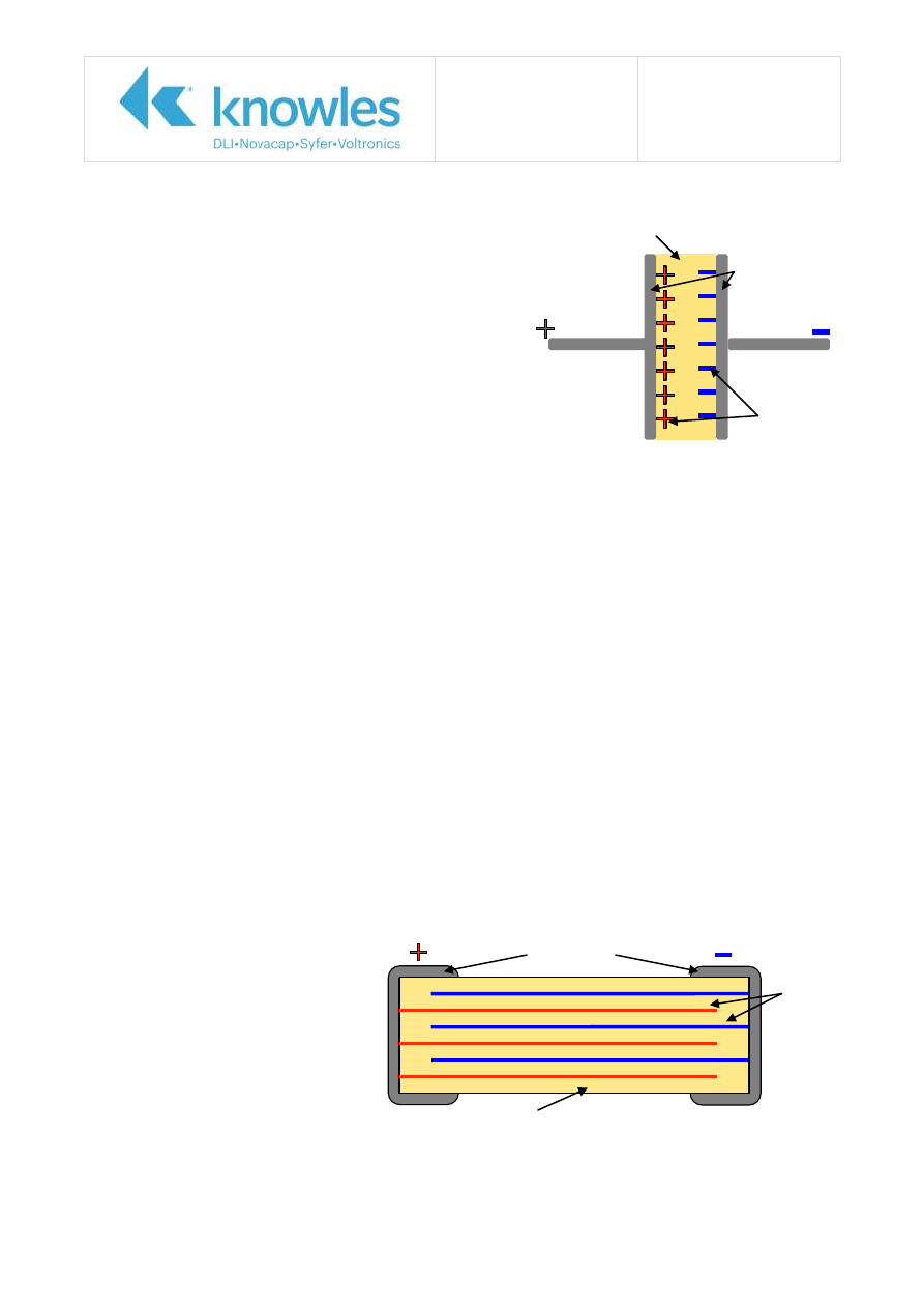
Construction
The most basic type of capacitor is a
single layer which is shown in Fig. 1 and
consists of a layer of dielectric material
sandwiched between a positive and a
negative electrode. The MLC capacitor,
which Syfer produce, takes this concept
and multiplies the number of layers to
increase the available capacitance
hence multilayer ceramic capacitor, see
Fig.2. Layers of ceramic are built up using a screen printing process, these are interleaved with
electrodes of alternating polarity. The like polarity electrodes are then joined together using a
Fig. 2
Dielectric
“Terminations”
Electrodes
Dielectric
Charge
Electrodes
Fig. 1

Application Note
Reference No: AN0034
Capacitor Basics Issue 3
Page 3 of 7
termination material. The termination can then be attached to wires or legs to form a radial leaded
MLCC or electroplated to form a surface mount MLCC.
MLCC Uses
A MLCC has many different applications in electronic circuits. However, the three main uses are:
Blocking:
A capacitor has dc voltage applied combined with a much smaller ac signal voltage. An important
application of capacitors is to stop direct current (dc) but allow alternating current (ac) from one
part of an electronic circuit to another. A dc voltage is blocked when the capacitor is charged but
if a varying (alternating positive and negative) voltage is applied then a current will flow first in
one direction, then in the other as the capacitor charges and discharges. You will find capacitors
used in this way in T.V. Radio and Audio Amplifiers.
Frequency Selection:
Capacitors are used to help detect Radio Frequency and they are part of the tuning circuit. Again,
they are used in T.V. and Radio circuits.
They can also be used to 'filter out' frequencies, which could interfere with the equipment.
Storage of Electrical Energy/Smoothing:
The ability of capacitors to store charge is used to stabilise the voltage to sensitive devices. This
application accounts for a large proportion of all MLCCs used. The capacitors are utilised close to
the memory chips in computers and ensures that the chip operating voltage stays constant in
spite of the electrical activity going on all around. The same property is used to smooth the
outputs from power supplies and voltage converters.
Limitations and Factors for Consideration
Capacitance (
C
) is:
Directly proportional to electrode overlap area (
A
)
A
C
Directly proportional to dielectric constant (
ε
r
)
r
ε
C
Inversely proportional to dielectric layer thickness (
T
)
T
C
1
Voltage rating is related to a non linear positive function of dielectric thickness.
f.T
V
w
These relationships have knock-on effects on the amount of capacitance available at set sizes and
voltages. Smaller footprint and restricted thickness limit the available capacitance value. Higher
voltage capacitors need greater dielectric thickness which means less capacitance, this is not a linear
function, especially for high voltage capacitors. For example, to increase the voltage from 1000V to
2000V requires a typical doubling of dielectric thickness; this in turn means that only half the number
of electrodes can fit into a set thickness. Due to the fact that capacitance is directly proportional to
overlap area and inversely proportional to dielectric thickness; the overall capacitance available in a
given size at 2000V is roughly 25% of that at 1000V.

Application Note
Reference No: AN0034
Capacitor Basics Issue 3
Page 4 of 7
Dielectric Types
There are many types of dielectric material each of which have their own characteristics and therefore
uses. Syfer use predominantly Barium Titanate and Neodymium Titanate based dielectric materials
which, in different formulations and designs make X5R, X7R, X8R, 2C1(BZ) and 2X1(BX) and C0G
materials, Syfer also have a High Q material. There is a trade off between ε
r
and stability and loss.
Generally speaking dielectrics with a higher ε
r
value, are less stable with temperature, time and voltage
than those with a lower ε
r
value. The main stability characteristics are defined as:
T
CC
– Temperature Coefficient of Capacitance, how much capacitance changes with temperature
V
CC
– Voltage Coefficient of Capacitance, how much capacitance changes with applied voltage
Ageing
– How much capacitance changes over time
DF and Q
– Dissipation Factor and Quality factor, reciprocals of each other and measure the
losses with the capacitor
The different material codes help define the performance of the dielectric material
EIA Class 2 Classification
Minimum
Temperature
Maximum
Temperature
Capacitance Change
Permitted
X -55
o
C
4 +65
o
C
A
±1.0%
Y -30
o
C
5 +85
o
C
B
±1.5%
Z -10
o
C
6 +105
o
C
C
±2.2%
7 +125
o
C
D
±3.3%
8 +150
o
C
E
±4.7%
9 +200
o
C
F
±7.5%
P
±10%
R ±15%
S
±22%
T
+22% / -33%
U
+22% / -56%
V
+22% / -82%
X7R
X7R is an EIA Class II dielectric; Syfer dielectric code ‘X’
The ‘X’ and ‘7’ define the lower and upper operational temperature range, i.e., -55
o
C and +125
o
C
respectively and ‘R’ defines the stability within the temperature range, in this case ±15%.
Dissipation factor is a maximum of 2.5%
V
CC
is unspecified for standard X7R material.
The ageing rate for X7R is typically 1% to 2% per time decade which means that, at 1% ageing, 2% of
the capacitance value will be lost between hour 10 and hour 1000. Syfer supply X7R capacitors to their
1000 Hour capacitance value.
X7R has a high ε
r
value of around 3000 and is used for capacitance values in the nF to μF range. X7R
capacitors are generally used in energy storage, smoothing and filtering applications.

Application Note
Reference No: AN0034
Capacitor Basics Issue 3
Page 5 of 7
X5R
X5R is an EIA class 2 dielectric Syfer dielectric code ‘P’.
X5R is generally similar to X7R except that the top operational temperature limit denoted by the ‘5’ is
+85°C.
X5R capacitors are used in similar applications to X7R but where the environmental conditions are
more stable.
X8R
X8R is an EIA class 2 dielectric
Syfer dielectric code ‘N’.
X8R is generally similar to X7R except that the top operational temperature limit denoted by the ‘8’ is
+150°C.
X8R capacitors are used in similar applications to X7R but where the environmental conditions require
stability at higher temperatures. Automotive under hood, industrial and down hole applications are
some examples.
2C1 (BZ) and 2X1 (BX)
Syfer dielectric codes ‘R’ and ‘B’.
These dielectric classifications are based on X7R dielectrics but include a V
CC
specification and a
different T
CC
requirement.
2C1 has T
CC
of ±20% and a V
CC
of +20%-30% with rated voltage applied.
2X1 has T
CC
of ±15% and a V
CC
of +15%-25% with rated voltage applied.
These dielectric classifications are useful where a more defined and stable capacitance value is
required.
C0G
C0G is an EIA Class I dielectric, it is also known as NP0, the Syfer dielectric code is ‘C’. C0G is much
more stable than the EIA Class 2 dielectrics.
T
CC
, C0G is defined as having an allowable capacitance change of ±30ppm/°C over the -55°C to
+125°C operational temperature range.
V
CC
, C0G is stable with voltage.
C0G has negligible ageing.
C0G has a lower DF, or higher Q than X7R, defined as a maximum of 0.15%. This means that when
operating at higher frequencies the power lost in the capacitor is reduced and it is less inclined to
overheat.
C0G dielectrics have ε
r
values of between 20 to 100 and are used to make stable lower capacitance
parts in the pF to nF region. These are typically used for filtering, balancing and timing circuits.
High Q
High Q is a C0G dielectric, the Syfer dielectric code is ‘Q’.
Generally similar to standard C0G except that the DF is lower/ Q is higher.
High Q material has a low ε
r
value and is used to make parts typically in the pF range, these are used
generally in high frequency applications which require low losses.
Application Note
Reference No: AN0034
Capacitor Basics Issue 3
Page 6 of 7
Useful Formulae and Calculations
DF
1
Q
Q is Quality Factor, DF is Dissipation Factor
fC
2
1
X
c
X
c
is Capacitive Reactance in Ohms, f is frequency in Hertz and C is capacitance in
Farads
c
s
DF.X
R
R
s
is Equivalent Series Resistance in Ohms, DF is Dissipation Factor and X
c
is Capacitive
Reactance in Ohms
R
I
P
2
P is Power dissipated in capacitor in Watts, I is rms current in Amps and R is R
s
in Ohms
Recognising a Syfer Part Number
A standard Syfer part number is 15 characters long, e.g., 1206J5000682KXT. This breaks down into:
Case Size Termination
Voltage
Capacitance Tolerance
Dielectric
Packaging
1206
J
500
0682
K
X
T
Case Size
1206
J 500 0682 K X T
The four case size characters represent the X and Y dimensions in thousandths of an inch.
Syfer’s range goes from 0402 (40 thou by 20 thou) to 8060 (800 thou by 600 thou).
Termination
1206
J
500 0682 K X T
Code ‘J’ is the industry standard glass frit type termination. Glass material loaded with silver is
applied to the ends of the capacitor. Sintered on at high temperature it ensures contact with the
ends of the internal electrodes. The termination is then electroplated with Nickel and Tin.
‘Y’ termination, trade name FlexiCap™, is the termination material which introduced the world
to flexible terminations. Pioneered by Syfer it protects the body of the capacitor from
mechanical stress. Polymer material loaded with Silver is cured onto the ends of the capacitor to
make an excellent bond with the internal electrodes. The termination is electroplated with Nickel
and Tin.
‘A’ and ‘H’ terminations are similar to ‘J’ & ‘Y’ respectively but are electroplated with a minimum
Lead content of 10%. (Used primarily in military and space applications to combat the potential
problem of tin whisker growth in certain environments.)
Termination codes ‘2’, ‘3’, ‘4’ and ‘5’ are the equivalent of ‘J’, ‘Y’, ‘A’ and ‘H’ terminations but
with a Copper barrier layer rather than Nickel. They provide a non-magnetic termination finish
with excellent solder leach resistance.
Code ‘F’ is an un-plated Silver Palladium loaded glass frit termination for non-magnetic and
epoxy bonding applications.
Voltage
1206
J
500
0682 K X T
010 – 999 are straightforward 10V to 999V, 1kV and above are in kV with the K as a decimal
point so 1K5 is 1.5kV up to 12K for 12kV.
Application Note
Reference No: AN0034
Capacitor Basics Issue 3
Page 7 of 7
Capacitance
1206
J 500
0682
K X T
The first three digits are significant figures and the fourth digit is a base 10 multiplier with the
final value being in picofarads (pF). For example 0682 = 068
10
2
= 6800pF
A ‘P’ or ‘N’ is used to specify fractions to denote the decimal point, so 4P70 would be 4.7pF and
12N4 would be 12.4nF
Tolerance
1206
J 500 0682
K
X T
C0G <10pF
C0G
10pF
X7R
H
0.05pF
F
1%
J
5%
B
0.1pF
G
2%
K
10%
C
0.25pF
J
5%
M
20%
D
0.5pF
K
10%
F
1.0pF
Dielectric Code
1206
J 500 0682 K
X
T
Class I
Class II
A – C0G to AEC-Q200
B – 2X1 (BX)
C – C0G
D – X7R to IECQ-CECC
F – C0G to IECQ-CECC E – X7R to AEC-Q200
Q – High Q
N – X8R
P – X5R
R – 2C1 (BZ)
X – X7R
Packaging
1206
J 500 0682 K X
T
‘T’ is taped and reeled on 178mm (7”) reels
‘R’ is taped and reeled on 330mm (13”) reels
‘B’ is bulk packed in tubs
For further information or technical assistance please contact our Sales Department on:
+44 (0)1603 723310 or by email at

AN0001 Issue 10 – FlexiCap™
CN# P109825
Termination
“An alternative termination material specifically designed to absorb greater
levels of mechanical stress thereby reducing capacitor failures associated
with mechanical cracking”
Introduction ............................................................................ 2
Queens Award for Innovation ................................................................... 3
..................................................................... 4
Customer Assembly Process Requirements ................................................ 5
Test Summary ......................................................................... 6
Key Electrical Characteristics ................................................................... 9
Additional Information .......................................................................... 10
Ordering Information – Standard MLCC Range ......................................... 11
Knowles (UK) Limited,
Old Stoke Road, Arminghall, Norwich,
Norfolk, NR14 8SQ, United Kingdom
Tel: +44 (0) 1603 723300
Tel. (Sales): 01603 723310
Fax: +44 (0) 1603 723301
www.knowlescapacitors.com/syfer
Application Note
Reference No.
AN0001 – FlexiCap™
Issue 10
Page 2 of 11
FlexiCap
™
Introduction
Syfer Technology Ltd introduced FlexiCap
™
in 1999 and became the first multilayer capacitor
manufacturer to offer a flexible termination to customers. This type of termination has proven to be
very successful as customers realize the benefits and also as demonstrated by other capacitor
manufacturers subsequently introducing flexible terminations, some with very similar names to
FlexiCap
™
.
FlexiCap
™
refers to the termination material that is applied over the electrodes. This material is a silver
loaded epoxy polymer that is applied using conventional termination techniques and then cured at
180ºC. Following the curing process, components are processed through the same manufacturing, test
and inspection stages when compared with the more traditional sintered terminated products.
Fired Ceramic
Dielectric
Tin
Intermediate
Outer
Nickel Layer
Termination
Layer
Base
Termination
Material
Metal
Electrodes
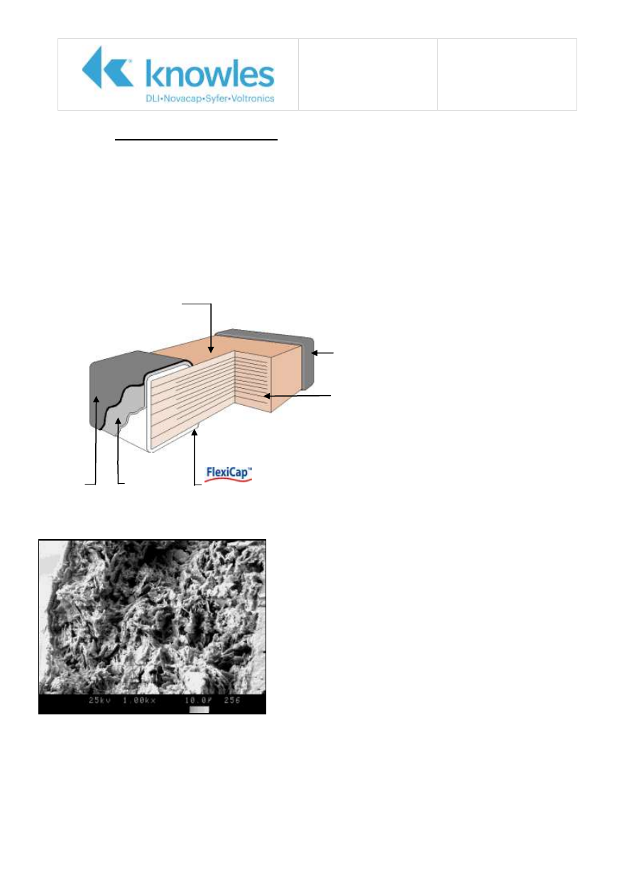
Picture taken at 1000x
magnification using a SEM showing
a fracture section through a
capacitor termination.
The picture demonstrates the
fibrous nature of the FlexiCap
™
termination that absorbs greater
levels of mechanical stress when
compared with standard sintered
silver termination.
Fig 1. Capacitor Construction

Application Note
Reference No.
AN0001 – FlexiCap™
Issue 10
Page 3 of 11
Queens Award for Innovation
The Queen's Awards for Enterprise are the UK's most prestigious awards for business performance. The
Awards are presented in three categories: International Trade, Innovation and Sustainable
Development
The Awards are made each year by The Queen, on the advice of the Prime Minister, who is assisted by
an Advisory Committee that includes representatives of UK Government, industry and commerce, and
the trade unions.
The Queens Award for Innovation recognizes companies that have demonstrated commercial success
through innovative products or services.
Her Majesty The Queen conferred the Queens Award for Innovation upon Syfer Technology Ltd in 2008
for recognition of outstanding achievements in Innovation with respect to FlexiCap
™
.
Application Note
Reference No.
AN0001 – FlexiCap™
Issue 10
Page 4 of 11
Benefits of Using FlexiCap
™
Sintered termination materials are fired onto the ceramic body of the component at approximately
800ºC. The result is a very hard material that provides minimal protection to the ceramic body of the
component with respect to mechanical strain when the component is situated on an assembly.
FlexiCap
™
termination material is a silver loaded epoxy polymer that is flexible and absorbs some of
the mechanical strain between the PCB and the ceramic component. Components terminated with
FlexiCap
™
withstand greater levels of mechanical strain when compared with sintered terminated
components
Types of mechanical strain where FlexiCap
™
terminated capacitors offer enhanced protection include
mechanical cracking (which is the largest cause for ceramic component failure) and also in applications
where rapid temperature changes can occur.
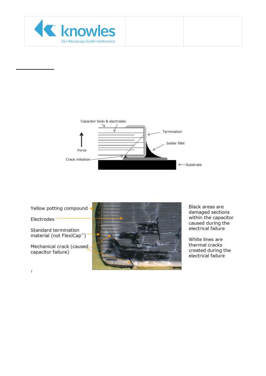
Mechanical Cracking
Due to its brittle nature, multilayer ceramic capacitors are more prone to excesses of mechanical stress
than other components used in surface mounting. One of the most common causes of capacitor
failures is directly attributable to bending of the printed circuit board (PCB) after solder attachment.
Excessive bending will create mechanical crack(s) within the ceramic capacitor. Mechanical cracks,
depending upon severity, may not cause capacitor failure during the final assembly test. Over time
moisture penetration into the crack can cause a reduction in insulation resistance and eventual
dielectric breakdown leading to capacitor failure in service.
Fig 1. Mechanical Crack
Application Note
Reference No.
AN0001 – FlexiCap™
Issue 10
Page 5 of 11
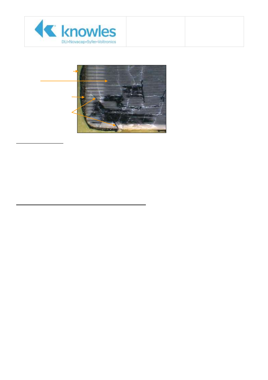
Example of a capacitor issued by a customer to Syfer for failure investigation:
Temperature Cycling
Rapid temperature changes when components are mounted on a PCB can induce stress as a result of
different material CTE (Coefficient of Thermal Expansion) rates. For example, a sintered terminated
component will typically fail a temperature cycle test consisting of 1000 cycles (-55ºC to 125ºC). The
difference in material (PCB, ceramic, solder) expansion rates can induce cracks within components that
cause components to electrically fail.
FlexiCap
™
termination absorbs some of the strain created during repeated rapid temperature changes
and components terminated with FlexiCap
™
pass temperature cycle tests such as 1000 cycles (-55ºC to
125ºC).
Customer Assembly Process Requirements
FlexiCap
™
terminated capacitors should be handled, stored and transported in the same manner as
sintered terminated capacitors. The requirements for mounting and soldering FlexiCap
™
terminated
capacitors are the same as for sintered terminated capacitors.
FlexiCap
™
components are compatible with lead solder applications and lead-free solder applications
with a maximum recommended reflow temperature of 270ºC.
FlexiCap
™
Moisture Sensitivity Level (MSL) = 1.
Yellow potting compound
Electrodes
Standard termination
material (not FlexiCap
™
)
Mechanical crack (caused
capacitor failure)
Black areas are
damaged sections
within the capacitor
caused during the
electrical failure
White lines are
thermal cracks
created during the
electrical failure
Application Note
Reference No.
AN0001 – FlexiCap™
Issue 10
Page 6 of 11
FlexiCap
™
Test Summary
FlexiCap
™
has been rigorously tested and approved/ qualified to the following test requirements:
Syfer qualification and ongoing routine tests.
IECQ-CECC QC32100 approval.
TUV Safety Capacitor approvals.
UL Safety Capacitor approvals.
AEC-Q200 qualification.
The key tests with respect to FlexiCap
™
performance are as follows.
Bend Test (Board Flex).
Method: Capacitor samples mounted onto a 100mm FR4 Test PCB and subjected to bend testing
in accordance with IEC 60068-2-21. Environmental testing: Test U: Robustness of
terminations and integral mounting devices or AEC-Q200-005.
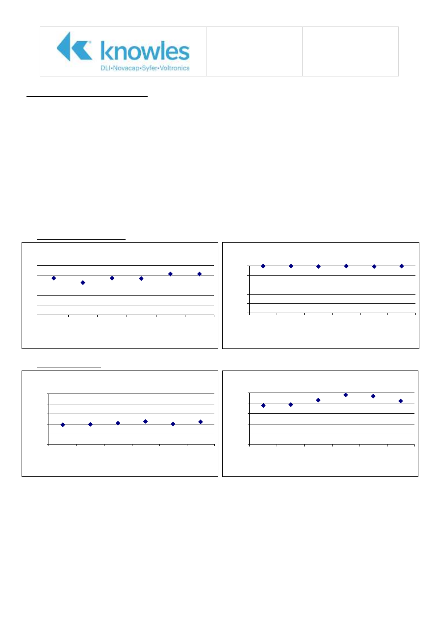
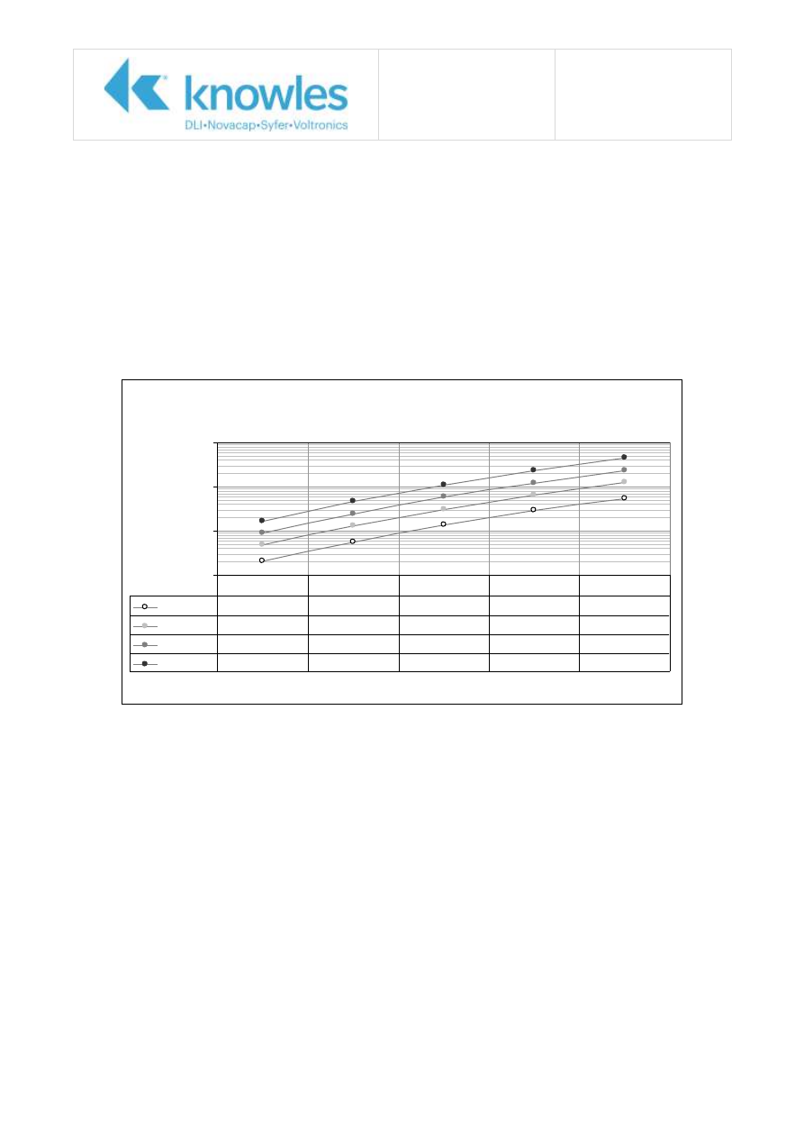
C0G (NP0) Performance
Mean Bend - C0G Sintered Termination (Code J)
0
2
4
6
8
10
0603 J
C0G
0805 J
C0G
1206 J
C0G
1210 J
C0G
1812 J
C0G
2220 J
C0G
Case Size
mm
Mean Bend - C0G
FlexiCap
Termination (Code Y)
0
2
4
6
8
10
0603 Y
C0G
0805 Y
C0G
1206 Y
C0G
1210 Y
C0G
1812 Y
C0G
2220 Y
C0G
Case Size
mm
(10mm maximum bend test equipment capability)
X7R Performance
Mean Bend - X7R Sintered Termination (Code J)
0
2
4
6
8
10
0603 J
X7R
0805 J
X7R
1206 J
X7R
1210 J
X7R
1812 J
X7R
2220 J
X7R
Case Size
mm
Mean Bend - X7R
FlexiCap
Termination (Code Y)
0
2
4
6
8
10
0603 Y
X7R
0805 Y
X7R
1206 Y
X7R
1210 Y
X7R
1812 Y
X7R
2220 Y
X7R
Case Size
mm
The bend test summary provides a comparison between component case sizes in the following
groups:
C0G (NP0) dielectric material with sintered termination material.
C0G (NP0) dielectric material with FlexiCap
™
termination material.
X7R dielectric material with sintered termination material.
X7R dielectric material with FlexiCap
™
termination material.
The bend tests conducted confirm that the FlexiCap
™
termination withstands greater mechanical
strain when compared with sintered termination materials.
Application Note
Reference No.
AN0001 – FlexiCap™
Issue 10
Page 7 of 11
Load (Life) Tests
Product type:
FlexiCap
™
X7R components
Time period analyzed:
11
th
June 2001 to 11
th
June 2009.
Test laboratory:
Syfer Technology Reliability Test Department.
Number of components tested: 71,614
Endurance test conditions:
1000 hours with 1.5x
(1)
rated voltage applied at 125
C.
Results:
178 failures in 71,614,000 component test hours.
Notes:
1).
1.5x rated voltage used during Syfer routine reliability tests. AEC-Q200 and IECQ-CECC
require 1.0x rated voltage. Product specific reliability data available on request.
The FIT (Failure In Time) rate graph provides an indication of component reliability in relation to a
customer’s application with respect to temperature and voltage being applied. For example, at 25ºC
and 50%RV (Rated Voltage), the FIT rate graph indicates 0.007 FITs. As a comparison, an automotive
customer specifies maximum of 0.1 FITs at 25ºC and 50%RV (Rated Voltage).
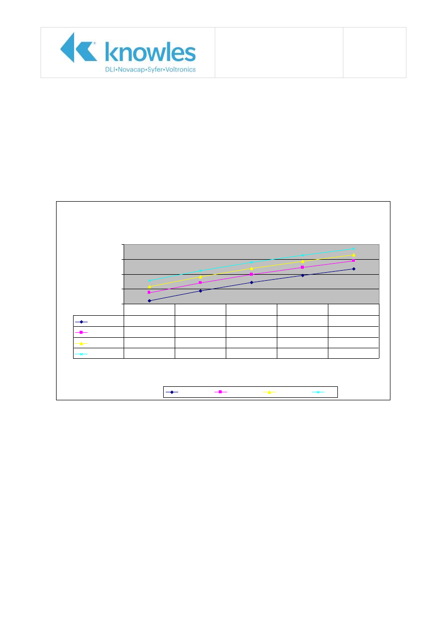
Termination Bend Performance - Endurance Testing
A sample of FlexiCap
™
terminated X7R capacitors has been subjected to 20,000 hours at 125
C.
Tests conducted after 20,000 hours indicated no deterioration in the electrical or mechanical
performance of the FlexiCap
™
termination.
A sample of FlexiCap
™
terminated X8R capacitors has been subjected to 5,000 hours at 150
C.
Tests conducted after 5,000 hours indicated no deterioration in the electrical performance.
Humidity Tests
From June 2001 to June 2009, a total of 27194 components (4,568,592 component test hours)
have been tested at 85
C @ 85RH for either 168hours or 1000hours. There have been 3 failures
that have not been attributed to FlexiCap
™
.
Failure rates at 60% confidence
0.00001
0.01
10
10000
FI
T
10% of RV
0.000
0.002
0.026
0.241
1.697
25% of RV
0.001
0.023
0.306
2.859
20.148
50% of RV
0.007
0.151
1.991
18.575
130.925
RV
0.048
0.982
12.937
120.704
850.754
25°C
50°C
75°C
100°C
125°C
Data derived fro m 178 failures in 71,614,000 co mpo nent test ho urs

Application Note
Reference No.
AN0001 – FlexiCap™
Issue 10
Page 8 of 11
In addition to the Syfer routine and AEC-Q200 tests, samples have been tested by an external test
laboratory for IECQ-CECC Damp Heat Steady State periodic test (56 days 40ºC/ 93%RH with
applied voltages of 0Vdc, 5Vdc or 50Vdc). Samples pass this test requirement.
Temperature Cycling
Temperature Cycle Profile: 40-minute cycle consisting of 10 minute ramp and 10 minute dwell at
temperature extremes.
Temperature Extremes:
-55
C to +125
C.
Number of Cycles:
1000.
Method:
Samples of FlexiCap
™
terminated
capacitors were soldered onto FR4 test PCB’s and
subjected to temperature cycling. After 1000 cycles, the capacitors were sectioned
mounted on the test PCBs for internal visual examination.
Results:
There were no cracks within the capacitors.
Passive Flammability Test
Method:
A sample of FlexiCap
™
terminated
capacitors were subjected to a needle flame test
in accordance with IEC 60384-1.
Requirement: Burning droplets of glowing parts falling down shall not ignite the tissue paper
(placed underneath the specimen being tested).
Results:
The sample passed the Passive Flammability Test.
Thermal Vacuum Outgassing Test
FlexiCap
™
material successfully passed ECSS-Q-70-02A Thermal vacuum outgassing test for the
screening of space materials. The test was conducted by an external test laboratory and results
are available in Syfer application note AN0026.
Customer Qualification
Samples of FlexiCap
™
terminated capacitors have been supplied to customers for qualification.
The qualifications conducted by customers have been successful and customer reaction to
FlexiCap
™
termination has been extremely favorable. Demand for FlexiCap
™
terminated capacitors
continues to increase as customers realize the advantages provided.
FlexiCap
™
terminated capacitors are supplied to many blue chip companies, O.E.M’s, E.M.S’s and
international component distributors. Applications include telecoms, military, aerospace,
automotive, industrial and power supplies.
Application Note
Reference No.
AN0001 – FlexiCap™
Issue 10
Page 9 of 11
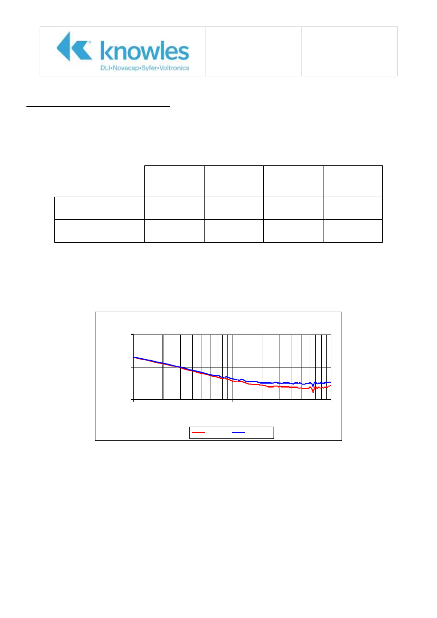
ESR v Frequency
0.010
0.100
1.000
1
10
100
Frequency (MHz)
E
S
R
(
O
h
m
s
)
FlexiCap
Standard
Key Electrical Characteristics
FlexiCap
™
terminated capacitors have equivalent electrical characteristics when compared with sintered
terminated capacitors.
For example (type 1812 100nF):
Capacitance
@ 1kHz
DF @ 1kHz
Resonant
Frequency
(RF)
Inductance
@ RF
Sintered
Termination
100.02nF
0.01167
14.468MHz
1.1965nH
FlexiCap
™
Termination
101.14nF
0.01173
14.468MHz
1.2099nH
The ESR characterisation of an 18nF 1825 X7R capacitor was undertaken to a frequency of 100MHz.
FlexiCap
™
and sintered termination were tested in parallel to determine the relative ESR performance.
From the graph below it can be seen that there is a reduction in ESR at high frequencies when
capacitors are terminated using FlexiCap
™
termination.
Application Note
Reference No.
AN0001 – FlexiCap™
Issue 10
Page 10 of 11
Additional Information
Syfer has generated a comprehensive range of application notes (available at
www.knowlescapacitors.com/syfer
) to provide additional information to customers.
Application notes that provide additional information with respect to FlexiCap
™
:
APPLICATION NOTE
CONTENTS
AN0002 Bend Testing
Test methods for Capacitor bend testing, and the
shape of typical cracks
AN0005 Mechanical Cracking
Potential causes of mechanical cracking, corrective
actions and depanelisation methods
AN0006 Dielectric Ageing
Capacitor dielectric ageing
AN0009 AEC-Q200 Stress Test Qualification
Provides information on tests performed by Syfer in
accordance with the AEC-Q200 specification
AN0010 Lead-free soldering and bend test
performance
The effects of Lead-free soldering on bend testing
through solder choice
AN0019 Tin Whiskers
Tin Whiskers mitigation and surface mount chip
capacitors
AN0021 Tandem Capacitors
Tandem capacitors terminated with FlexiCap™
provide an ultra robust and reliable component.
AN0022 Open Mode Capacitors
Open mode capacitors terminated with FlexiCap™
provide a robust component that fail in an open
circuit mode.
AN0024 Moisture Sensitivity Level Classification
for Syfer products
MSL classification IPC / JEDEC J-STD-020D for Syfer
products.
AN0026 Outgassing test results for FlexiCap™
capacitors
Results for ECSS-Q-70-02A outgassing tests on
FlexiCap™ capacitors.
AN0028 Soldering / Mounting Chip Capacitors,
Radial Leaded Capacitors and EMI Filters
This gives guidance to engineers and board designers
on mounting and soldering Syfer products.

Application Note
Reference No.
AN0001 – FlexiCap™
Issue 10
Page 11 of 11
Ordering Information – Standard MLCC Range
1210
Y
100
0103
J
X
T
Chip Size
Termination
Voltage d.c.
(marking code)
Capacitance in Pico
farads (pF)
Capacitance
Tolerance
Dielectric
Codes
Packaging
Suffix Code
0603
0805
1206
1210
1808
1812
1825
2220
2225
3640
5550
8060
Y
= FlexiCap
TM
termination base with
nickel barrier (100%
matte tin plating).
RoHS compliant.
H
= FlexiCap
TM
termination base with
nickel barrier (tin/lead
plating with min. 10%
lead).
Not RoHS compliant.
F
= Silver Palladium.
RoHS compliant
J
= Silver base with
nickel barrier (100%
matte tin plating).
RoHS compliant
A
= Silver base with
nickel barrier (tin/lead
plating with min. 10%
lead).
Not RoHS compliant
010
= 10V
016
= 16V
025
= 25V
050
= 50V
063
= 63V
100
= 100V
200
= 200V
250
= 250V
500
= 500V
630
= 630V
1K0
= 1kV
1K2
=1.2kV
1K5
=1.5kV
2K0
= 2kV
2K5
=2.5kV
3K0
=3kV
4K0
=4kV
5K0
=5kV
6K0
=6kV
8K0
=8kV
10K
=10kV
12K
=12kV
<1.0pF
Insert a P for the decimal
point as the first character.
e.g.,
P300
= 0.3pF
Values in 0.1pF steps
≥1.0pF & <10pF
Insert a P for the decimal
point as the second
character.
e.g.,
8P20
= 8.2pF
Values are E24 series
≥10pF
First digit is 0.
Second and third digits are
significant figures of
capacitance code.
The fourth digit is the
number of zeros following.
e.g.,
0101
= 100 pF
Values are E12 series
H
: ± 0.05pF
(only available for
values <4.7pF)
<10pF
B
: ± 0.10pF
C
: ± 0.25pF
D
: ± 0.5pF
F
: ± 1.0pF
≥10pF
F
: ± 1%
G
: ± 2%
J
: ± 5%
K
: ± 10%
M
: ± 20%
C
= C0G/NP0
(1B)
X
= X7R
(2R1)
P
= X5R
T
= 178mm
(7”) reel
R
= 330mm
(13”) reel
B
= Bulk pack
– tubs or trays
Used for specific
customer
requirements
For quotations please contact Syfer Sales Department

AN0002 Issue 7 – Bend Testing
CN# P109825
Bend Testing
Methods and International Specifications
International Requirements/ Specifications ..................................................2
Capacitor Bend Tests Conducted on Syfer Product ........................................3
Mechanical Crack Shape ............................................................................7
Knowles (UK) Limited,
Old Stoke Road, Arminghall, Norwich,
Norfolk, NR14 8SQ, United Kingdom
Tel: +44 (0) 1603 723300
Tel. (Sales): 01603 723310
Fax: +44 (0) 1603 723301
www.knowlescapacitors.com/syfer

Application Note
Reference No: AN0002
Bend Testing
Issue 7
Page 2 of 8
Introduction
Due to its brittle nature, multilayer ceramic capacitors are more prone to excesses of mechanical stress
than other components used in surface mounting. One of the most common causes of capacitor
failures is directly attributable to the bending of the printed circuit board (PCB) after solder
attachment. Excessive bending will create mechanical stress within the ceramic capacitor that, if
sufficient, can result in mechanical cracks.
The purpose of this report is to provide details regarding:
International Specifications that define bend test methods and acceptability.
Methods employed by Syfer to measure the mechanical performance of the termination
material.
The shape of cracks created by PCB bending - mechanical stress.
International Requirements/ Specifications
The international requirement for bend testing is referred to in several different specifications.
1.
IEC 60384-1:2001 Fixed capacitors for use in electronic equipment Part 1: Generic Specification
section 4.35 Substrate bending test refers to IEC 60068-2-21.
2.
IEC 60068-2-21: 2006 Environmental testing: Test U: Robustness of Terminations and Integral
Mounting Devices. Section 8 test Ue specifies the test required to assess the mechanical
robustness of surface mounting device terminations when mounted on a substrate. Test Ue
1
specifies the substrate bend test.
The purpose of test Ue
1
is to verify that the capacitors can withstand bending loads that are
likely to be applied during normal assembly or handling operations.
IEC 60068-2-21 refers to requirements such as deflection and acceptance criteria as being
included in the “relevant specification”. Syfer maintains IECQ CECC (International
Electrotechnical Commission Quality certification programme- CENELEC Electronic Components
Committee) product approval and the “relevant specification” is QC 32100-A001:2007.
3.
QC 32100-A001:2007 Table 2 – Periodic Tests defines board flex minimum requirements as:
COG: All types, X7R: Y and H only (Flexicap™)
3mm deflection Class I
2mm deflection Class II
X7R (non – Flexicap
™
termination) 1mm deflection
4.
AEC-Q200-005, Board Flex / Terminal Bond Strength Test.
Minimum requirements stated in table 2 stress test reference 21: 2mm (min) for all except
3mm for Class I.
Application Note
Reference No: AN0002
Bend Testing
Issue 7
Page 3 of 8
Capacitor Bend Tests Conducted on Syfer Product
Currently there are 2 methods employed by Syfer to measure the mechanical performance of capacitor
termination when mounted on a substrate:
1.
External Test Laboratory
To maintain IECQ-CECC product approval (certified by BSI “British Standards Institute”) Syfer
issues capacitor samples to an external test laboratory for a variety of tests to be conducted in
accordance with IECQ CECC requirements. The external test laboratory is not part of Syfer and
has full traceability to International Reference Standards.
Syfer has maintained IECQ-CECC product approval for >20 years.
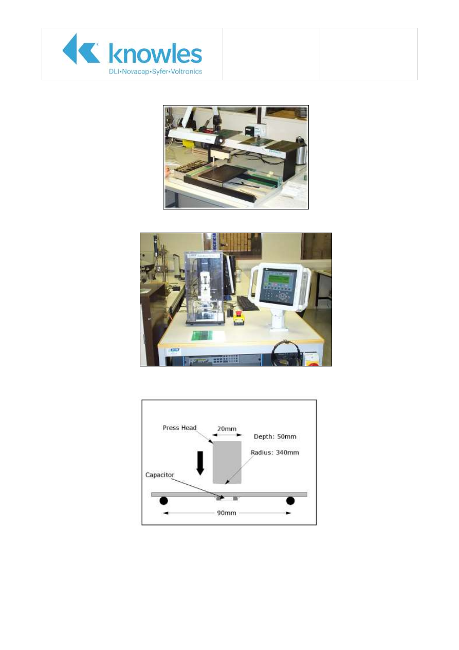
2. Syfer Bend Tests
In addition to the external test laboratory Syfer also conducts bend tests. Samples of capacitors
are mounted onto FR4 Test PCBs using 62/36/2 Sn/Pb/Ag solder and subjected to bend testing
in accordance with IECQ CECC or AEC –Q200-005 (depending on termination and dielectric
types.
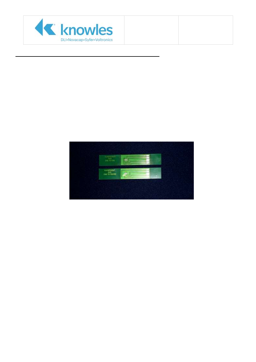
Example of FR4 Test PCB Used
Application Note
Reference No: AN0002
Bend Testing
Issue 7
Page 4 of 8
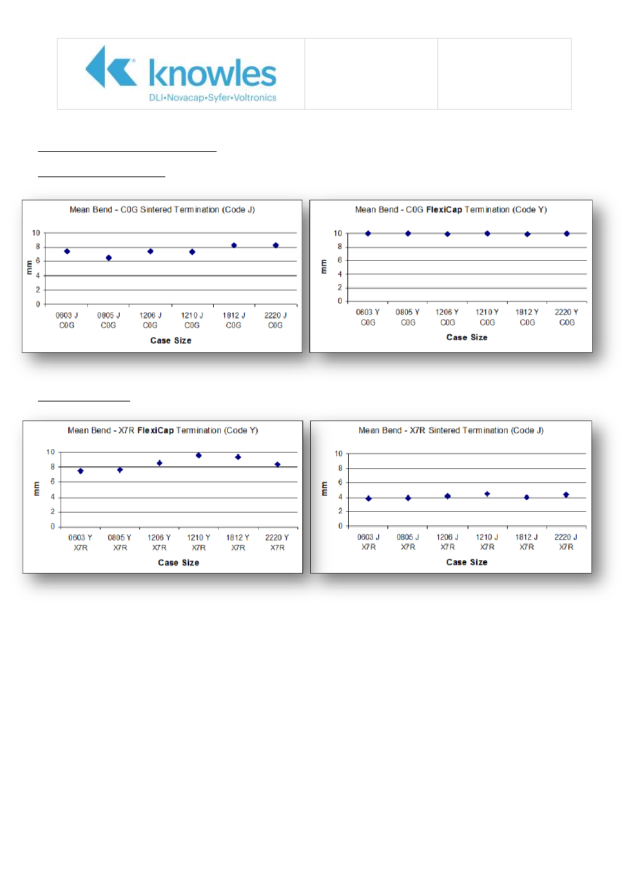
Capacitor Placement Method
Syfer’s Bend Test Facility
Fig 1. Bend Test Method
Application Note
Reference No: AN0002
Bend Testing
Issue 7
Page 5 of 8
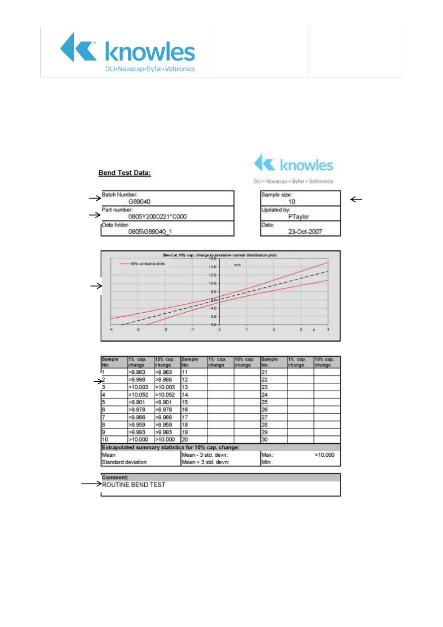
A minimum of 10 Test PCBs (depending on test requirements) are used for each bend test. Each
PCB is mounted with one capacitor and deflected automatically until the capacitor breaks. The
software analyses the change in capacitance measured by the Agilent 4288A capacitance meter. As
soon as the capacitance change is greater than 10% the bend is recorded in mm.
The results of the test are saved to the Syfer network but also can be communicated as a printed
document as below.
Document shows the results for Flexicap™ terminated components
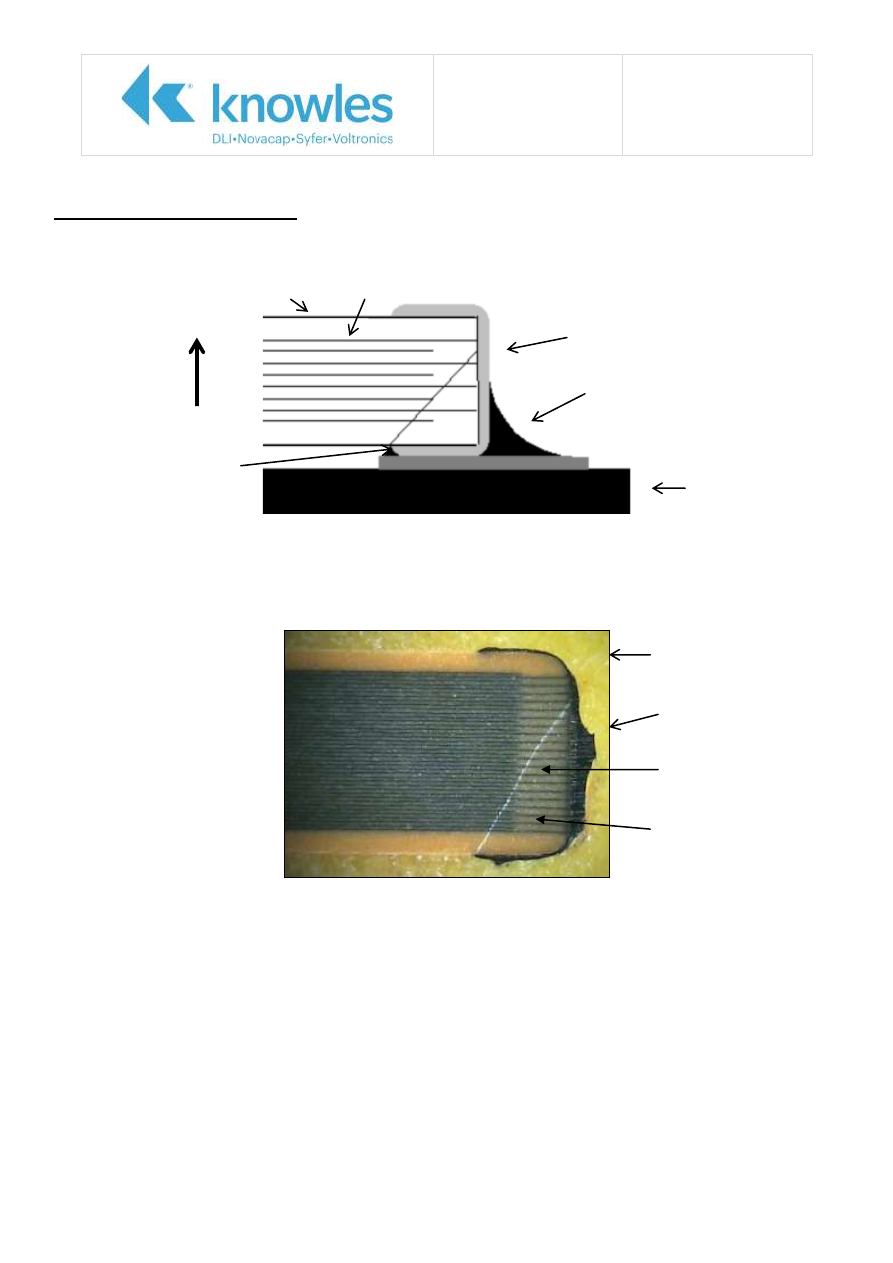
Syfer Batch No:
Syfer Part No:
Distribution Plot
Sample Size
Measured Results
Type of Test
Application Note
Reference No: AN0002
Bend Testing
Issue 7
Page 6 of 8
Bend Test Performance Summary
C0G (NP0) Performance
X7R Performance
The bend test summary provides a comparison between component case sizes in the following groups:
C0G (NP0) dielectric material with sintered termination material.
C0G (NP0) dielectric material with FlexiCap™ termination material.
X7R dielectric material with sintered termination material.
X7R dielectric material with FlexiCap™
termination material.
The bend tests conducted confirm that the FlexiCap
™
termination withstands greater mechanical strain
when compared with sintered termination materials.
(10mm maximum bend test equipment capability)
Application Note
Reference No: AN0002
Bend Testing
Issue 7
Page 7 of 8
Mechanical Crack Shape
By conducting extensive bend testing capacitor manufacturers including Syfer have demonstrated that
mechanical stress applied by bending the PCB results in a distinctive type of crack within the capacitor.
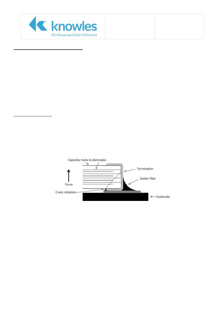
Fig 2. Mechanical Crack
During Syfer’s investigation into mechanical cracking over 15000 capacitors were subjected to bend testing.
Example of capacitors issued by customers to Syfer for failure investigation:
Capacitor body & electrodes
Termination
Solder fillet
Substrate
Force
Crack initiation
Yellow potting compound
Termination & solder
Mechanical crack
Electrodes

Application Note
Reference No: AN0002
Bend Testing
Issue 7
Page 8 of 8
Summary
Syfer capacitors pass the International Specifications for bend testing. In addition to routine
tests conducted at Syfer an external test laboratory conducts periodic IECQ CECC tests on Syfer
product including bend testing.
The crack created by mechanical stress during PCB bending is a distinctive type of crack.
For further information regarding:
a)
Potential causes for mechanical cracking refer to Syfer application note “Mechanical Cracking”
application note reference AN0005.
b)
Flexicap
™
. Refer to “Flexicap™ Termination” application note reference AN0001.
c)
AEC-Q200. Refer to “AEC-Q200 Stress Test Qualification for Passive Components” application
note reference AN0009.
Information is also available on Syfer’s web site
www.knowlescapacitors.com/syfer

AN0004 Issue 10 – Quality & Reliability Data
CN# P109825
Quality & Reliability Data
Section 2 - Test Conditions ...................................................................... 4
Section 3 - F.I.T. Rate Data ..................................................................... 5
Acceleration Factor Calculations ............................................................... 5
C0G Capacitor Reliability Data ................................................................. 6
FIT (Failure In Time) Rate Graph .............................................................. 6
X7R Capacitor Reliability Data .................................................................. 7
FIT (Failure In Time) Rate Graph .............................................................. 7
Knowles (UK) Limited,
Old Stoke Road, Arminghall, Norwich,
Norfolk, NR14 8SQ, United Kingdom
Tel: +44 (0) 1603 723300
Tel. (Sales): 01603 723310
Fax: +44 (0) 1603 723301
Email:
Web:
www.knowlescapacitors.com/syfer

Application Note
Reference No. AN0004
Reliability & Quality
Issue 10
Page 2 of 7
Section 1 - Introduction
The major influence, within Syfer Technology Limited, is to provide its Customers with 'World Class'
capacitors.
Syfer has developed its own unique 'Wet Process' for the manufacture of Multilayer Ceramic Chip
Capacitors. This has been in operation for some 30 years, significantly increasing the reliability levels
obtained today, over those that were the expectation then.
Syfer's 'Wet Process' is based upon the principle of Screen Printing, both ceramic and electrode layers, in a
single operation. This gives a more consistent deposition and greater accuracy of electrode alignment. In
contrast to parts made by 'Tape Methods', it reduces stresses within the components.
At all manufacturing stages, well defined controls are in place. Statistical Process Control (SPC) techniques
are used extensively to monitor and to reduce process variability.
Microsections are prepared from each batch of product built. Destructive Physical Analysis (DPA) is
conducted on each microsection to verify structural integrity and the absence of voids, delaminations or
other defects.
After the fabrication cycle, 100% testing is conducted for:
(1)
Capacitance
(2)
Dissipation Factor
(3)
Insulation Resistance
(4)
Voltage Proof
Syfer's Quality Control Function audits each process stage and the outgoing products, to ensure strict
conformity to internal, customer, national and international specifications.
Syfer holds IECQ-CECC, TUV, UL, ISO9001, ISO14001 and OHSAS18001 approvals.

Application Note
Reference No. AN0004
Reliability & Quality
Issue 10
Page 3 of 7
In addition to its advanced construction methods, and sophisticated Quality Controls, Syfer carries out
regular long term accelerated tests on its products to prove their reliability.
The Capacitor Industry accepts that no single test, in isolation, is an effective measure of total reliability
and, therefore, accelerated testing, directed at selected capacitor performance factors, is conducted, by
Syfer, on a regular basis. This includes:
(1)
125
o
C Endurance Testing
at 1.5 times rated voltage
(2)
85
o
C/85% Relative Humidity Testing
at stress voltages of 1.5, 5 and 50 vdc
Syfer maintains its rigorous test regime, to give its customers useful and detailed data on the reliability of
its products. There is a continuing trend toward higher value capacitors in all major dielectric categories as
circuit designers have demanded even greater volumetric capacity. This has prompted an increase in the
number of 'high' value lots tested; now approximately 20% of such parts are tested compared with 10%
for standard product. The results presented here reflect this change in product mix.
Each section of this document describes the methodology of test and includes a summary of the results
obtained. F.I.T. Rate Data is shown, based upon Endurance Test results.
The aim of this document is to confirm that Syfer continues to maintain its reputation for the manufacture
of products that meet, and exceed, customer's expectations of reliability.
Syfer's Quality and Technical personnel are available to discuss this information, on request.

Application Note
Reference No. AN0004
Reliability & Quality
Issue 10
Page 4 of 7
Section 2 - Test Conditions
Endurance
Duration
1000 Hours
Intermediate Check Time
168 Hours
Voltage
1.5 x Rated Voltage
Current Limitation
Each component stressed via a 100kΩ resistor
Temperature
C0G125
o
C
X7R125
o
C
Post Test Limits
Insulation Resistance C0G
4000MΩ or 40s
X7R
2000MΩ or 50s
(whichever is the less)
85°C / 85%RH
Duration
168 Hours
Voltage Bias
Rated voltage up to a maximum of 50 volts dc, however, when specified,
1.5Vdc or 5Vdc may be required
Current Limitation
Each component stressed via a 100kΩ resistor
Temperature
85°C
Relative Humidity
85%
Post Test Limits
Insulation Resistance
C0G
4000MΩ or 40s
X7R
2000MΩ or 50s
(Whichever is the less)
Application Note
Reference No. AN0004
Reliability & Quality
Issue 10
Page 5 of 7
Section 3 - F.I.T. Rate Data
Acceleration Factor Calculations
where
and
where
E
a
= Activation energy (1.0 eV for M.L.C's)
k
= Boltzmann' Constant (8.617 x 10
-5
eV/K)
T
= Temperature in K (273 + Temperature in
o
C)
Failure Rates at the Specified Confidence Level (60%) are derived from:
where
FR
= Estimated Failure Rate at Use Stress
X
2
= Chi Square calculated for number of rejects at test stress
H
= Component test hours
Conversion Factors
From
To
Operation
FITS
MTBF (Hours)
10
9
FITS
FITS
MTBF (Years)
10
9
(FITS
8760)
AF
x
AF
=
(AF)
Factor
on
Accelerati
e
temperatur
voltage
V
V
=
Factor
on
Accelerati
use
stress
2.7
voltage
T
T
E
e
Factor
on
Accelerati
stress
use
a
1
1
k
e
temperatur
H
x
AF
1
x
2
X
=
FR
2

Application Note
Reference No. AN0004
Reliability & Quality
Issue 10
Page 6 of 7
C0G Capacitor Reliability Data
Product type:
C0G capacitors.
Time period analyzed:
1
st
January 2010 to 31
st
December 2010
Test laboratory:
Syfer Technology Reliability Test Department
Number tested:
17,450
Test conditions:
1000 hours with 1.5x rated voltage applied at 125
C
Results:
4 failures in 17,450,000 component test hours
FIT (Failure In Time) Rate Graph
The FIT (Failure In Time) rate graph provides an indication of component reliability in relation to a
customer’s application with respect to temperature and voltage being applied. For example, at 25ºC and
50%RV (Rated Voltage), the FIT rate graph indicates 0.002 FITs. As a comparison, an automotive
customer specifies maximum of 0.1 FITs at 25ºC and 50%RV (Rated Voltage).
2010 C0G
(
FIT Rates Calculated at 60% Confidence Level)
(Data derived from 17,450,000 component test hours from which there were 4 failures)
0.0000
0.0010
0.1000
10.0000
1000.0000
FI
Ts
10% of RV
25% of RV
50% of RV
RV
10% of RV
0.0000
0.000
0.006
0.052
0.36
25% of RV
0.0002
0.005
0.065
0.61
4.3
50% of RV
0.002
0.032
0.43
4.0
28
RV
0.010
0.21
2.8
26
182
25°C
50°C
75°C
100°C
125°C
Application Note
Reference No. AN0004
Reliability & Quality
Issue 10
Page 7 of 7
X7R Capacitor Reliability Data
Product type:
X7R capacitors.
Time period analyzed:
1
st
January 2010 to 31
st
December 2010
Test laboratory:
Syfer Technology Reliability Test Department
Number tested:
24,778
Test conditions:
1000 hours with 1.5x rated voltage applied at 125
C
Results:
11 failures in 24,778,000 component test hours
FIT (Failure In Time) Rate Graph
The FIT (Failure In Time) rate graph provides an indication of component reliability in relation to a
customer’s application with respect to temperature and voltage being applied. For example, at 25ºC and
50%RV (Rated Voltage), the FIT rate graph indicates 0.002 FITs. As a comparison, an automotive
customer specifies maximum of 0.1 FITs at 25ºC and 50%RV (Rated Voltage).
2010 X7R
(
FIT Rates Calculated at 60% Confidence Level)
(Data derived from 24,778,000 component test hours from which there were 11 failures)
0.0000
0.0010
0.1000
10.0000
1000.0000
FI
Ts
10% of RV
25% of RV
50% of RV
RV
10% of RV
0.0000
0.001
0.008
0.071
0.50
25% of RV
0.0003
0.007
0.091
0.85
6.0
50% of RV
0.002
0.045
0.59
5.5
39
RV
0.014
0.29
3.8
36
252
25°C
50°C
75°C
100°C
125°C

AN0005 Issue 5 – Mechanical Cracking
CN# P109825
Mechanical Cracking
The Major Cause for Multilayer Ceramic Capacitor Failures
Exceptional Circumstances ...................................................................... 3
Normal Circumstances ............................................................................ 3
Assembly Design/ Manufacture Considerations ........................................... 4
Review Production Processes ................................................................... 5
Syfer Capacitor Enhancements Offered ..................................................... 6
Depaneling Methods ............................................................................... 7
Knowles (UK) Limited,
Old Stoke Road, Arminghall, Norwich,
Norfolk, NR14 8SQ, United Kingdom
Tel: +44 (0) 1603 723300
Tel. (Sales): 01603 723310
Fax: +44 (0) 1603 723301
www.knowlescapacitors.com/syfer
Application Note
Reference No: AN0005
Mechanical Cracking
Issue 5
Page 2 of 7
Introduction
Due to its brittle nature, multilayer ceramic capacitors are more prone to excesses of mechanical stress
than other components used in surface mounting. One of the most common causes of capacitor
failures is directly attributable to bending of the printed circuit board (PCB) after solder attachment.
Excessive bending will create mechanical crack(s) within the ceramic capacitor. Mechanical cracks,
depending upon severity, may not cause capacitor failure during the final assembly test. Over time
moisture penetration into the crack can cause a reduction in insulation resistance and eventual
dielectric breakdown leading to capacitor failure in service.
Figure 1: Mechanical Crack
Example of capacitors issued by customers to Syfer for failure investigation:

Application Note
Reference No: AN0005
Mechanical Cracking
Issue 5
Page 3 of 7
Potential Causes
Mechanical cracks are created by excessive mechanical stress after the capacitors have been soldered
onto the substrate.
Excessive mechanical stress can be the result of the following:
Exceptional Circumstances
Interference fit. For example, physical abuse.
Normal Circumstances
Assembly design.
Board de-paneling causing the PCB to bend.
Automatic test equipment employing a “bed of nails” as contacts. Faults often occur at, or in
close proximity to, support pillars within the test jig. Vacuum fixtures can also cause excessive
PCB bend.
PCB distortion/ warp caused by storage conditions or uneven PCB designs. Frequently distorted
PCBs are straightened after the soldering process causing the capacitors to mechanically crack.
Radial/ through hole component insertion especially if there is a tight fit between the radial
leads and PCB hole.
Attachment of rigid fixtures such as heat sinks.
Fitting IC’s, connectors into solder mounted sockets with no support.
Methods of transportation/ storage and handling during process stages allowing the PCB to
bend.
Fixing completed sub-assemblies into the final assembly. For example, employing a snap fit
operation or by over-tightening fixing screws.
Application Note
Reference No: AN0005
Mechanical Cracking
Issue 5
Page 4 of 7
Corrective Actions
Extensive bend tests performed at Syfer including bench-marking against competitor’s products has
proven that:
i.
Syfer capacitors pass the International Specifications
(1)
defining robustness of termination
criteria.
ii.
the bend test performance of Syfer’s sintered termination capacitors is comparable with
competitor’s sintered termination product.
(1)
For International Specifications and Syfer Bend Test Methods refer to Syfer Application Note
AN0002 Bend Testing.
The only effective methods of resolving mechanical cracking issues are:
i.
reduce the mechanical stress being exerted on the capacitors.
ii.
and/ or increasing the process window so that the mechanical stress exerted onto the ceramic
section of the capacitor is reduced.
ATE, functional tests and reliability tests have limited success in identifying capacitor failures caused by
mechanical cracking.
Assembly Design/ Manufacture Considerations
Mechanical stress can be influenced by a number of different factors associated with the design of the
assembly and assembly manufacture. These factors include:
PCB design – copper power and ground planes.
A PCB design resulting in an uneven metal distribution (usually caused by large power or
ground planes) can result in PCB warpage during the soldering process caused by the different
Thermal Coefficient of Expansion rates between the copper and the epoxy fiber glass. If large
power/ ground planes are required then cross hatching the copper area may prove to be useful.
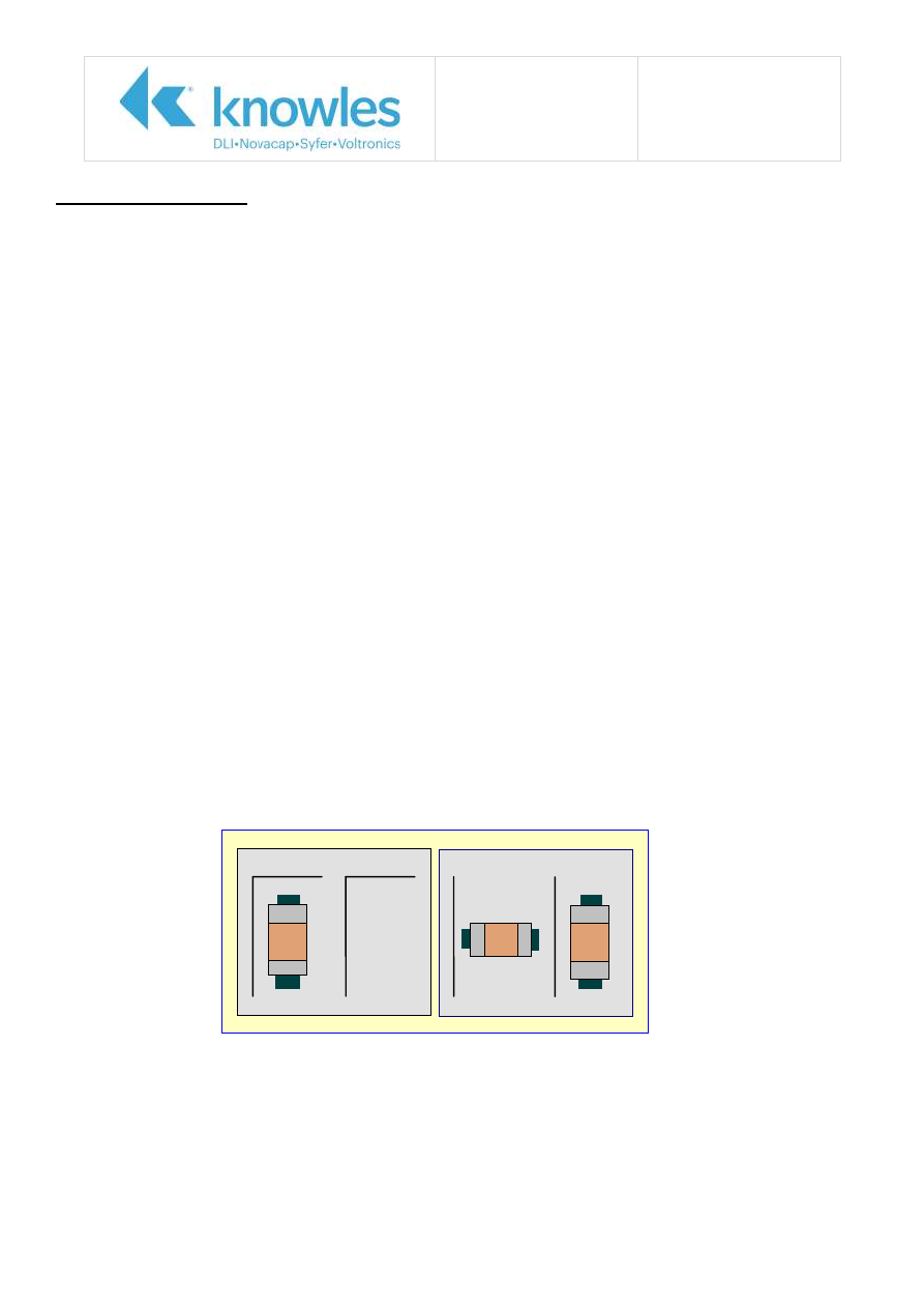
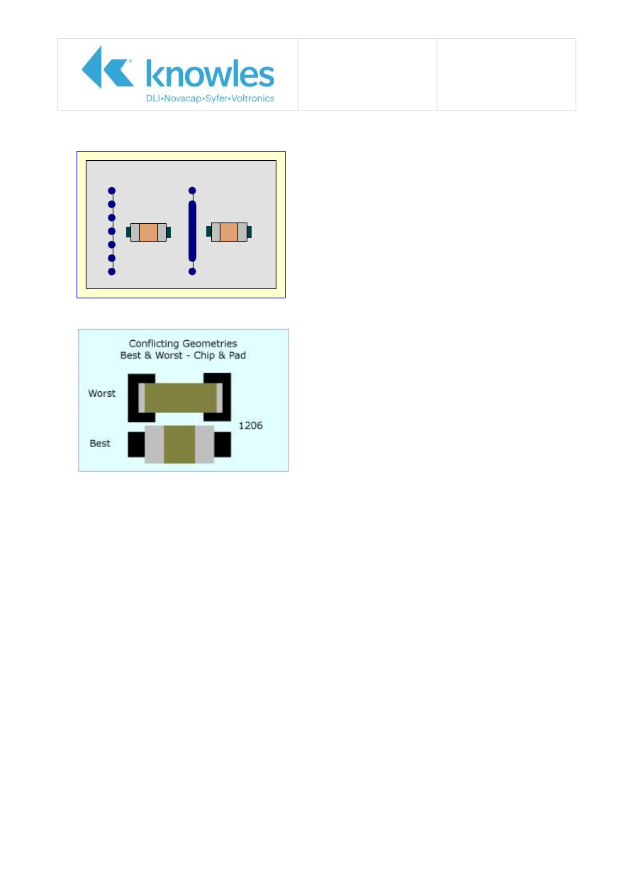
Position/ orientation of the capacitor on the PCB in relation to the edge of the PCB and other
components/ attachments.
Recommended capacitor
orientation with respect to
PCB edge (denoted by black
lines).
Note: Stress zone is typically
within 5mm of PCB edge or
fixing point.
Capacitor
placement not
recommended in
the corner of the
PCB.
PCB Corner
PCB Edge
Incorrect
Correct
Incorrect
Correct
Application Note
Reference No: AN0005
Mechanical Cracking
Issue 5
Page 5 of 7
Use of PCB slots
Solder pad/ land sizes
Use of Adhesives.
Depending upon the type of adhesive used, the effect can be a significant reduction in the bend
strength of a capacitor. For example, during experiments approximately 50% of the PCB bend
was required to crack a capacitor fixed with adhesive when compared to a capacitor not fixed
with adhesive.
Review Production Processes
Mechanical cracking occurs after the capacitors have been soldered into position. Subsequent flexing of
the PCB creates mechanical stress within the capacitor that if sufficient can result in the capacitor
being mechanically cracked.
When mechanical cracking has been identified as the cause for capacitor failures the typical approach
for customers is to review the production process for any obvious process stage including handling and
transportation that may be bending the PCB. If no obvious stage is identified then the next step is to
remove samples of capacitors from assemblies at different process stages and then subject the
capacitors to sectioning/ internal examination to determine if the capacitors have been cracked. The
shape of mechanical cracks is shown in Fig.1.
Incorrect
Correct
Reducing the pad/ land size can reduce the
level of stress exerted onto the capacitor
by approximately 50%.
Using a slot along the depanelisation edge
reduces the level of stress exerted onto the
capacitor by approximately 50%.

Application Note
Reference No: AN0005
Mechanical Cracking
Issue 5
Page 6 of 7
An example of a typical investigation would be to remove capacitors from assemblies after completing
the following stages:
Soldering
Depanelisation
Insertion of radial components including connectors and IC’s into sockets
ATE
Fixing the completed sub-assembly into the final assembly.
Syfer Capacitor Enhancements Offered
Syfer offers a polymer termination that effectively reduces the mechanical stress being exerted onto
the ceramic section of the capacitor by approximately 50%. The polymer termination is being used by
a variety of customers and requires no changes to the customer’s assembly process.
For further details refer to Syfer Application Note AN0001 Polymer.
Test Methods
There is no 100% guaranteed method for being able to test capacitors that have been mechanically
cracked. The success of the tests conducted relies on the extent of the mechanical cracks – wider
cracks are more likely to fail.
Examples of tests conducted by customers:
Dry Heat/ Steady State. Assemblies powered in a hot dry environment to accelerate the
breakdown of the capacitors.
Damp Heat/ Steady State. Assemblies powered in a hot humid environment to try to drive
moisture into the crack and cause capacitor failure.
Temperature Cycling. Assemblies are temperature cycled with the purpose of opening the crack
to cause capacitor failure.
Vibration and Shock. Assemblies are subjected to vibration/ shock tests with the purpose of
opening the crack to cause capacitor failure.
X-Ray. Customers have tried to employ x-ray solder joint inspection equipment to try to detect
mechanical cracks with very limited success.
Scanning Acoustic Microscopy.
The tests conducted have depended upon the equipment available to customers and the success of
tests has varied.
Application Note
Reference No: AN0005
Mechanical Cracking
Issue 5
Page 7 of 7
Depaneling Methods
Depaneling is the process of separating individual PCBs from a main panel (usually after the soldering
operation) and can present a high risk of mechanically cracking ceramic capacitors. There are various
depaneling methods employed, some of which present a greater risk when compared to other
methods.
As a guide, depaneling methods include:
Depaneling Method
Benefits
Negatives
Comments
Manual Break-Out
Flexibility.
No tooling costs/ changes.
No software set-up.
High risk of mechanical cracks.
Labour intensive.
Not consistent.
Potentially high scrap rate.
Not generally recommended
though frequently used
Scissor Shearing/
Guillotine
Low tooling costs.
Minimal/ no software set-up.
Ease of operation.
Severe shock – high risk of
mechanical cracks.
Potentially high scrap rate.
Not generally recommended.
Blanking/ Die
Shearing/ Punch-Out
Fast processing times.
Virtually any PCB shape.
High tooling costs.
Potential for shock – depending
upon supporting fixtures.
Less flexibility – tooling changes
required.
Usually used for processing high
volume of assemblies.
Circular Rolling
Blades
Low tooling costs.
Minimal/ no software set-up.
Ease of operation.
Less stress exerted when
compared with Shearing.
Some machines are operator
dependant. For example, operators
hold PCB sides – excessive
mechanical stress can still be
created.
Frequently used by customers
processing low to moderate
volume of assemblies.
Sawing
Wedge-shaped knives shear
panel with gentle rocking motion
along the whole length of the
section to be cut – less stress
exerted.
Some machines are operator
dependant. For example, operators
hold PCB sides – excessive
mechanical stress can still be
created.
Exerts less mechanical stress
when compared with manual,
guillotine, blanking and circular
blades.
Routing
Flexibility.
Virtually any PCB shape.
Reduces mechanical stress.
No/ minimal tooling changes
required.
Good quality PCB edge finish.
Software set-up.
Relatively slow processing times.
Initial costs when compared with
some of the other depaneling
systems.
Exerts less mechanical stress
when compared with manual,
guillotine, blanking and circular
blades.
Laser Cutting
Flexibility.
Virtually any PCB shape.
No mechanical stress.
No/ minimal tooling changes
required.
Initial costs and maintenance
costs.
Depaneled edge often charred and
can be jagged.
Extra cleaning process possibly
required to remove charring.
Very good regarding no
mechanical stress but is costly
and not frequently used by
customers.
Water Jet
Flexibility.
Virtually any PCB shape.
*No mechanical stress.
No/ minimal tooling changes
required.
Initial costs and maintenance
costs.
Process can be slow.
Noisy operation.
Water removal and treatment
environmental issues.
* There are conflicting reports
regarding the level of stress
exerted onto the PCB.
Also, water jets appear to be
rarely used.
When reviewing depaneling methods it is recommended that customers contact equipment
manufacturers to help evaluate what type of system is most suitable based on processing times,
flexibility, costs and mechanical stress exerted.

AN0006 Issue 6 - Capacitance Ageing
CN# P109825
Capacitance Ageing of
Ceramic Capacitors
Explanation of the natural ageing process resulting in logarithmic loss of Capacitance
Measuring Equipment and Measurement Uncertainties
Capacitance Tolerance & Circuit Application
Appendix 1 Tolerance Correction For Ageing Rates of 1% and 6%
Knowles (UK) Limited,
Old Stoke Road, Arminghall, Norwich,
Norfolk, NR14 8SQ, United Kingdom
Tel: +44 (0) 1603 723300
Tel. (Sales): 01603 723310
Fax: +44 (0) 1603 723301
www.knowlescapacitors.com/syfer
Application Note
Reference No: AN0006
Capacitance Ageing
Issue 6
Page 2 of 8
Introduction
Capacitor ageing (Capacitance Drift) is a term used to describe the negative, logarithmic capacitance
change that takes place in ceramic capacitors with time. The ageing process has a negligible affect on
Class 1 (C0G) product but should be taken into account when measuring Class 2 (X7R, Y5V & Z5U)
product.
The crystalline structure for Barium Titanate based ceramics changes on passing through its Curie
temperature (known as the Curie Point) at approximately 125
o
C. The domain structure relaxes with
time and in doing so, the dielectric constant reduces logarithmically, this is known as the ageing
mechanism of the dielectric constant. The more stable dielectrics have the lowest ageing rates.
The start point for the ageing process is indicated for all product supplied by Syfer by the date stated
on the packaging labels. If the ageing start point is not known then the ageing process can be reset by
heating the capacitors to a temperature above the Curie Point. The ageing process then starts again
from zero.
Law of Capacitance Ageing
During the first hour after cooling through the Curie temperature, the loss of capacitance is not well
defined, but after this time it follows a logarithmic law that can be expressed in terms of an ageing
constant.
The ageing constant '
k
', or ageing rate, is defined as the percentage loss of capacitance due to the
ageing process of the dielectric that occurs during a decade of time (a tenfold increase in age) and is
expressed as percent per logarithmic decade of hours. As the law of decrease of capacitance is
logarithmic, this means that in a capacitor with an ageing rate of 1% per decade of time, the
capacitance will decrease at a rate of:
i)
1% between 1 and 10 hours
ii)
an additional 1% between the following 10 and 100 hours
iii)
an additional 1% between the following 100 and 1,000 hours
iv)
an additional 1% between the following 1,000 and 10,000 hours etc.
The ageing rate continues in this manner throughout the capacitors life.
An alternative method of expressing this is that the percentage loss of capacitance will be 2 times '
k
'
between 1 and 100 hours and 3 times '
k
' between 1 and 1,000 hours. This may be expressed
mathematically by the following equation:
C
t
=
C
1
1 -
k
log
10
t
100
Application Note
Reference No: AN0006
Capacitance Ageing
Issue 6
Page 3 of 8
Where:
C
t
is the capacitance t hours after the start of the ageing process
C
1
is the capacitance 1 hour after the start of the ageing process
k
is the ageing constant in percent per decade (as defined above)
t
is the time in hours from the start of the ageing process
The ageing constant may be declared by the manufacturer for a particular ceramic dielectric, or it may
be determined by de-ageing the capacitor and measuring the capacitance at two known times
thereafter.
Typical values of the ageing constant for Syfer Technology ceramic capacitors are:
Dielectric Class
Typical Value
C0G (CG/1B)
Negligible
X7R (2C1)
1 to 2% per decade
Example of a different dielectric material/ type offered by other capacitor manufacturers:
Dielectric Class
Typical Value
Z5U (2F4)
6% per decade
Capacitance Measurements
Ageing Allowances
Because of ageing, it is necessary to specify an age for reference measurements at which the
capacitance shall be within the prescribed tolerance. This is fixed at 1,000 hours, since for practical
purposes there is not much further loss of capacitance after this time.
In order to calculate the capacitance C
1000
after 1,000 hours the following formula may be used:
C
1000
=
C
t
1 -
k
( 3 - log
10
t )
100

Application Note
Reference No: AN0006
Capacitance Ageing
Issue 6
Page 4 of 8
For measurements during the course of capacitor manufacture, the loss of capacitance from the time of
measurement to the 1,000 hour age will be known and can be off-set by using asymmetric inspection
tolerances. For example, if it is known that the total capacitance loss to 1,000 hours will be 5%, then
the capacitors may be inspected to limits of say -15%/+25% instead of ± 20%.
All capacitors shipped are within their specified tolerance at the standard reference age of 1,000 hours
after cooling through their Curie temperature.
Ageing begins after cooling from above the Curie point and continues, apparently forever. This
capacitance loss does not limit the effective life of the capacitor, however, it should not be overlooked.
A 1% change of capacitance value between 1 and 10 hours may seem serious but 1% change between
10,000 and 100,000 hours is less significant.
Refer to Appendix 1 showing the tolerance correction (for standard reference age of 1,000 hours) to
allow for ageing rates of 1% and 6% between 12 and 10,000 hours.
Ageing Allowance Example
A capacitor with a tolerance of ± 20% is measured after 3750 hours from its last heat cycle. The
corrected tolerance limits to which it should be tested are:
a) For 1% ageing; tolerance correction is:
-0.6%
Therefore, tolerance range allowed is:
-20.6% to +19.4%
b) For 6% ageing; tolerance correction is:
-3.4%
Therefore, tolerance range allowed is:
-23.4% to +16.6%
Test Temperature
Capacitance is normally declared at a reference temperature, this varies according to specification
dependent on country of origin, for example CECC specifies 20
C ± 2
C.
Capacitors measured at Syfer are tested in accordance with CECC specifications at 20
C. If capacitors
are tested at a different temperature then allowances should be made when verifying the capacitance
value.
Care should be taken when testing capacitors. Errors can arise if capacitors are heated by body heat
through handling and it is recommended that for precision measurement plastic tweezers be used to
handle capacitors.
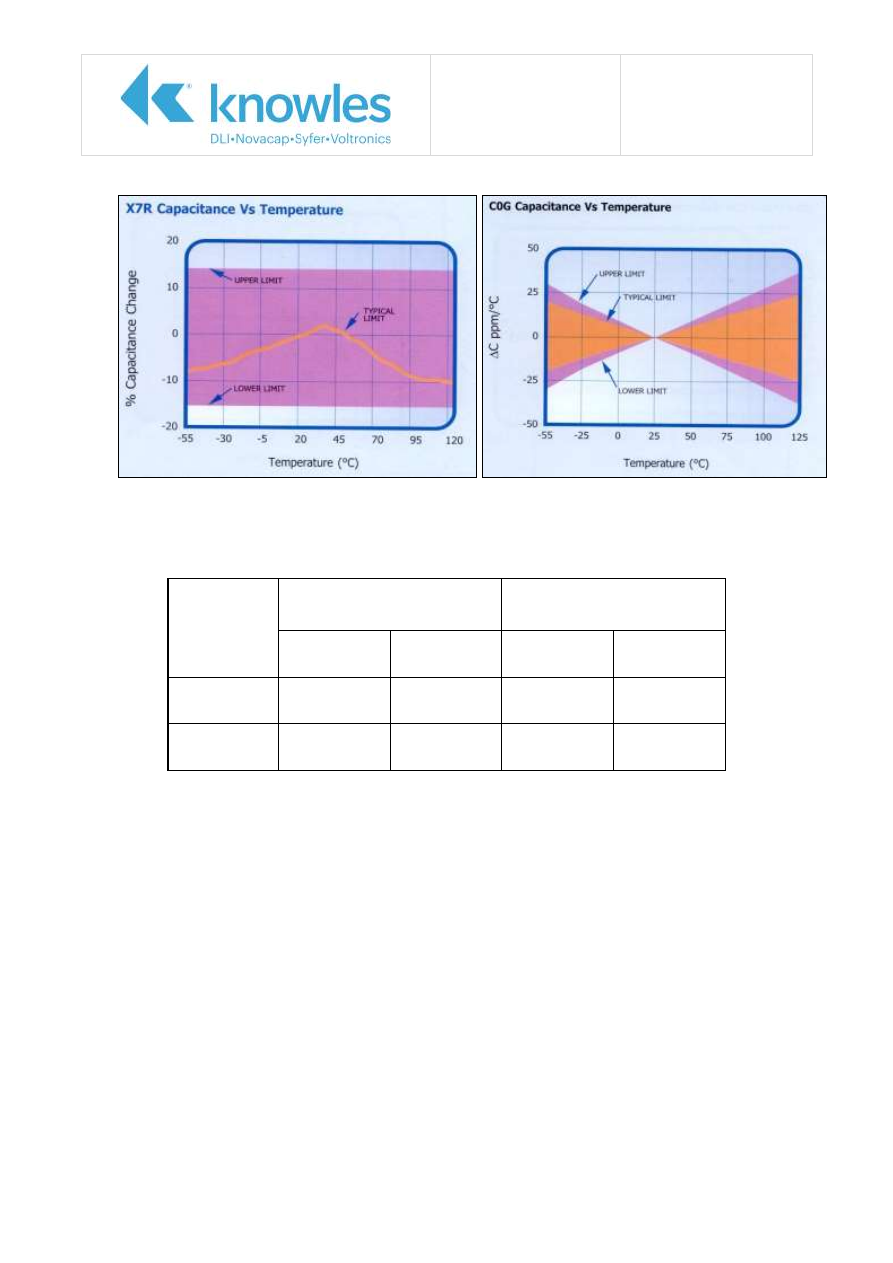
Application Note
Reference No: AN0006
Capacitance Ageing
Issue 6
Page 5 of 8
Test Frequency and Voltage
The following table details the frequency and voltage settings used for electrical testing of surface
mount and radial product types by dielectric classification.
Dielectric
Class
Surface Mount
Radial product
Test
Frequency
Test Voltage
(rms)
Test
Frequency
Test Voltage
(rms)
C0G (CG/1B)
1nF = 1kHz
<1nF = 1MHz
1.0V
1kHz
1.0V
X7R (2C1)
1kHz
>25V = 1.0V
25V = 0.5V
1kHz
0.5V
Measuring Equipment and Measurement Uncertainties
Incorrect capacitance measurement can also be introduced as a result of either the accuracy of the
equipment and/ or measurement uncertainties.
Measuring equipment. The accuracy and precision of the measuring device/ meter should be
examined to determine if the meter is capable of measuring the capacitor adequately.
Measurement uncertainties. Errors should be removed before measuring the capacitors. For
example, by performing open and short-circuit compensations.
Low capacitance measurements can be affected by stray capacitance from equipment test
leads. It is recommended that when measuring values less than 50pF test fixtures are used to
minimise the possibility of stray capacitance.
As a result of the piezoelectric nature of ceramic capacitors, tweezer pressure can also affect
capacitance measurements.
Low capacitance radial products can also be affected by stray capacitance from the components
legs/ leads. It is recommended that radial products are measured across the leads directly next
to the component body.

Application Note
Reference No: AN0006
Capacitance Ageing
Issue 6
Page 6 of 8
Resetting the Ageing Process
For Class 1 (C0G) ceramics the ageing rate is negligible. For Class 2 ceramics it may be necessary to
reset the ageing process.
The ageing process is reset by heating the dielectric above its Curie Point. To ensure that all capacitors
have been sufficiently heated and that the ageing process has been reset it recommended that
capacitors are placed in an oven @ 160
C for 1½ hours separated on a metal tray. After the heating
process, the capacitors should then be allowed to stabilise at room temperature (20
C ± 2
C) for 24
hours before capacitance measurements are conducted.
Capacitance Tolerance & Circuit Application
Capacitance ageing is inherent in class 2 ceramic capacitors and it is important for circuit designs to
recognise and allow for this effect. It is of particular importance when initial capacitance tolerance must
be tight. In these circumstances the ageing rate may cause the capacitors to drift out of tolerance on
the low side. For example, it would be imprudent to specify a 5% tolerance for a unit with a 2% ageing
rate.
Designing the capacitor with an initial value large enough to compensate for long term ageing will
cause the units to be out of tolerance on the high side each time de-ageing occurs. This can be
especially true for equipment where an ambient operating temperature of +125
o
C could cause
potential de-ageing. For this reason tight tolerance capacitors should be of class 1 dielectric when
possible.
Summary & Conclusions
1.
Electrical Tests. The recommended sequence for testing Multilayer Ceramic Capacitors is:
i)
Insulation Resistance (IR)
ii)
Voltage Proof (VP)/ Dielectric Withstand Voltage (DWV)
iii)
De-age Class 2 capacitors and allow to stabilise at room temperature for 24 hours before
capacitance measurements are conducted.
iv)
Capacitance, apply factors based on the manufacturers ageing rate and the time elapsed
since the last Curie temperature excursion.
v)
Dissipation Factor.
vi)
Other Tests. If any limits are specified for change in capacitance during a long term test,
the capacitor should be de-aged before both the initial and final measurements.
2.
With surface mount MLC's some of the solder termination materials used will diffusion bond at
temperatures close to that of the ceramic Curie temperature. It is, therefore, important that
when de-ageing these products they should be placed on a tray such that their termination end
surfaces are not in contact with each other.
3.
The ageing process is completely repeatable and predictable for a given capacitor.
4.
Capacitance change is negative and logarithmic in respect to time.
5.
Application of a D.C. bias can move the point on the ageing curve forward in time. When a D.C.
voltage is applied at elevated temperatures (below the Curie Point) the capacitor will show a
loss of capacitance but with a consequently lower ageing rate.
6.
Class 1 CG/1B (C0G) dielectric has a negligible ageing rate.
7.
Class 2 ceramic dielectrics have ageing rates which may vary from 0.6% to 8%. Dependent
upon particular ceramic composition employed, this wide capacitance change, as a result of

Application Note
Reference No: AN0006
Capacitance Ageing
Issue 6
Page 7 of 8
'Shelf' ageing and temperature cycling, illustrates why tight-tolerance (less than ± 5%) high
dielectric constant ceramics should only be specified with caution.
8.
Soldering both leaded and surface mount class 2 capacitors into a circuit will, because of the
ageing phenomenon, give an increase in capacitance as a result of the soldering temperature
being greater than the dielectric Curie Point. The magnitude of the change will be dependent on
the soldering temperature, time and the dielectric class.
Application Note
Reference No: AN0006
Capacitance Ageing
Issue 6
Page 8 of 8
Appendix 1 Tolerance Correction For Ageing Rates of 1% and 6%
For Standard Reference Age Of 1,000 Hours
Hours Since
Last Heat Cycle
1%
6%
Hours Since
Last Heat Cycle
1%
6%
12
1.9
11.5
1000
0.0
0.0
14
1.9
11.1
1050
0.0
-0.1
16
1.8
10.8
1100
0.0
-0.2
18
1.7
10.5
1150
-0.1
-0.4
20
1.7
10.2
1200
-0.1
-0.5
22
1.7
9.9
1250
-0.1
-0.6
24
1.6
9.7
1300
-0.1
-0.7
26
1.6
9.5
1350
-0.1
-0.8
28
1.6
9.3
1400
-0.1
-0.9
30
1.5
9.1
1450
-0.2
-1.0
32
1.5
9.0
1500
-0.2
-1.1
34
1.5
8.8
1600
-0.2
-1.2
36
1.4
8.7
1700
-0.2
-1.4
38
1.4
8.5
1800
-0.3
-1.5
40
1.4
8.4
1900
-0.3
-1.7
45
1.3
8.1
2000
-0.3
-1.8
50
1.3
7.8
2100
-0.3
-1.9
55
1.3
7.6
2200
-0.3
-2.1
60
1.2
7.3
2300
-0.4
-2.2
65
1.2
7.1
2400
-0.4
-2.3
70
1.2
6.9
2500
-0.4
-2.4
80
1.1
6.6
2600
-0.4
-2.5
90
1.0
6.3
2700
-0.4
-2.6
100
1.0
6.0
2800
-0.4
-2.7
120
0.9
5.5
2900
-0.5
-2.8
140
0.9
5.1
3000
-0.5
-2.9
150
0.8
4.9
3250
-0.5
-3.1
175
0.8
4.5
3500
-0.5
-3.3
200
0.7
4.2
3750
-0.6
-3.4
225
0.6
3.9
4000
-0.6
-3.6
250
0.6
3.6
4250
-0.6
-3.8
275
0.6
3.4
4500
-0.7
-3.9
300
0.5
3.1
4750
-0.7
-4.1
350
0.5
2.7
5000
-0.7
-4.2
400
0.4
2.4
5250
-0.7
-4.3
450
0.3
2.1
5500
-0.7
-4.4
500
0.3
1.8
5750
-0.8
-4.6
550
0.3
1.6
6000
-0.8
-4.7
600
0.2
1.3
6500
-0.8
-4.9
650
0.2
1.1
7000
-0.8
-5.1
700
0.2
0.9
7500
-0.9
-5.3
750
0.1
0.7
8000
-0.9
-5.4
800
0.1
0.6
8500
-0.9
-5.6
900
0.0
0.3
9000
-1.0
-5.7

AN0007 Issue 5 – Stack Chips
CN# P109825
Stack Chip Components
Handling and Usage
Knowles (UK) Limited,
Old Stoke Road, Arminghall, Norwich,
Norfolk, NR14 8SQ, United Kingdom
Tel: +44 (0) 1603 723300
Tel. (Sales): 01603 723310
Fax: +44 (0) 1603 723301
www.knowlescapacitors.com/syfer

Application Note
Reference No: AN0007
Stack Chip Components
Handling and Usage
Issue 5
Page 2 of 4
Storage and Transportation
A selected number of components are available ‘Tape and Reel’ packed. The storage and handling of
these components is as for normal chip capacitors.
Unless supplied ‘Tape and Reel’ packed, all stack chip components will be supplied packed in a
protective foam environment in individual cells, to prevent damage by contact during transportation.
It is recommended that the components are stored in the original packing until used.
If stored in the original packing, the components should be able to withstand all reasonable handling
associated with transportation.
When removing components from the packaging, care must be taken to prevent damage to the legs
due to snagging. The recommended method of removal is :
Carefully remove the foam packing pieces individually from the box.
When the loaded packing piece is on the bench, gently push each component from
the packing piece onto the bench.
Do not allow the components to drop.
It is preferable to place empty packing pieces on the bench, so as to protect units as
they are removed.
Take special care when removing ‘L’ leaded components, as the legs will be sandwiched between
packing pieces. If the components are removed from the wrong side of the packing piece, damage will
occur to the legs.
Under no circumstances should the components be gripped with pliers, or similar, to remove them
from the packing. This is liable to cause severe damage to the component and may effect reliability.
Handling and Usage
The components should always be handled with care (see mechanical considerations).
Recommended pad designs for surface mounted and SM leaded components are available from Syfer
on request.
These components are designed for assembly using all proprietary soldering methods such as hot air
reflow or vapour phase soldering. Surface mount and SM leaded components are NOT considered
suitable for assembly using a soldering iron – particularly ‘J’ leaded devices - as damage will almost
certainly occur due to the thermal shock caused by the proximity of the soldering iron to the ceramic
capacitors. If hand soldering is necessary, a hot air pencil should be carefully used, following the
guidelines below. ‘S’ leaded components may be suitable for assembly with a soldering iron, provided
the iron is applied to the opposite side of the boards to the component, and sensible care is taken as to
the choice of iron tip and temperature settings.
On surface mount leaded components, any solder fillet should be to maintained to the foot of the leg
(that part in contact with the board) only. Any meniscus to the vertical leg should be minimised to
prevent the solder from reinforcing the leg and preventing the optimum stress decoupling from
occurring.
The soldering process should be controlled such that the component does not experience any thermal
shocks that may induce cracks into the ceramic dielectric.
The pre-heat temperature rise of the component should be kept to around 2
O
C per second. In practise
successful temperature rises tend to be in the region of 1.5
O
C to 4
O
C per second dependant upon the
substrate and components. The pre-heat temperature should be close to the maximum soldering
temperature (within 50
O
C minimum) and the component should be stable at the pre-heat temperature
prior to the final rise to reflow temperature.
Application Note
Reference No: AN0007
Stack Chip Components
Handling and Usage
Issue 5
Page 3 of 4
Reflow time should be minimised, and the temperature controlled to a maximum of 220
O
C.
Cooling to ambient temperature should be allowed to occur naturally. Natural cooling allows a gradual
relaxation of the thermal mismatch stresses in the solder and epoxy joints. Draughts should be
avoided. Forced air cooling can induce thermal breakage, and cleaning with cold fluids immediately
after a soldering process may result in cracked components. If soldering jigs have been used for
support and to control the temperature gradients, the components should not be removed from the
jigs until cooling to ambient temperature is complete.
The components are compatible with solder types Sn60 / Sn62 or similar. Leaded components are
compatible with typical lead free solder alloys such as SAC. Unleaded components, terminated with
PdAg termination, may exhibit leaching with lead free solders and we recommend that customers carry
out their own trials.
The components are designed to be compatible with conventional cleaning processes – but it is the
customers responsibility to ensure that there is compatibility with any specific cleaning solvents or
processes.
Mechanical Considerations
These components, by their very nature, are large, delicate pieces of ceramic. All multi element, and
large area, ceramic components should be considered fragile and handled with appropriate care. Any
product dropped or mishandled should be considered suspect and only used advisedly.
Designers should also consider the geometry and relatively high mass of this type of component.
Devices that are mis-specified, and unsuitable for use, may be susceptible to damage in high vibration
or shock environments. This may be dramatic to the extent of leg or stack shearing. Tall multi chip
stacked components, where the height / base aspect ratio is particularly high, are especially at risk.
Dependant on the intended use, it may be advisable to strap, or otherwise support, the device, to
ensure satisfactory operation. If strapping is used, then care must be taken to ensure that the ceramic
is not cracked or chipped by excessive pressure exerted by the strap. If it is considered preferential to
support the chip by the use of an adhesive to bond the component to the substrate, then care must be
taken to ensure that there are no thermal mismatch stresses exerted on the ceramic by this bond.
The use of stand off legs on the larger components will provide a degree of stress relief during such
operations as board de-panalisation, and may help prevent cracking occurring if board flexing takes
place.
Thermal Considerations
The soldering requirements for these components are given earlier (see Handling Considerations).
All these components are large when compared to conventional ceramic capacitors. This size makes
the ceramic potentially susceptible to thermal shock cracking if they are subjected to rapid changes of
temperature, as temperature deltas can be generated within the build of the capacitors, causing a build
up of stress.
It is not possible to state specific limits for the rate of temperature change, as this will be largely
dependant on such factors as the thermal mass of the substrate to which the component is mounted
and the degree to which the component is shielded from direct exposure to severe temperature
environments. However, the rate of temperature change should be restricted to < 4
O
C / second in all
cases.
The main causes of thermal cracking is mismatched Coefficients of Thermal Expansion (CTE) between
the capacitors and their surrounding environment. For example a capacitor mounted directly onto a
PCB will have a different CTE to the PCB upon which it is mounted. As the assembly undergoes
temperature changes, the board and the capacitor expand and contract at different rates, causing a
build up of stress at the interconnection point. If the rate of temperature change is too great, or the
CTE mismatch too great, then the stress build up at this point may be sufficient to cause cracking of
the ceramic in the assembly.

Application Note
Reference No: AN0007
Stack Chip Components
Handling and Usage
Issue 5
Page 4 of 4
This effect worsens as the assemblies increase in size, as the stress force acts over a greater area. For
this reason we do not recommend mounting chip sizes >= to 3640 directly to boards, but advocate the
use of stand off legs for these components.
The use of stand off legs will minimise any reaction between the capacitor assembly and any PCB by
allowing the legs to compensate for mismatch by flexing.

AN0008 Issue 4 – Restricted Substances
CN# P109825
Restricted Substances and
Lead-free Soldering
End-of Life Vehicle (ELV) Directive
Restriction on Hazardous Substances (RoHS) Directive
Material content in Syfer Capacitors
Knowles (UK) Limited,
Old Stoke Road, Arminghall, Norwich,
Norfolk, NR14 8SQ, United Kingdom
Tel: +44 (0) 1603 723300
Tel. (Sales): 01603 723310
Fax: +44 (0) 1603 723301
www.knowlescapacitors.com/syfer

Application Note
Reference No: AN0008
Restricted Substances
Issue 4
Page 2 of 11
Introduction
Due to increasing environmental concerns a number of restrictions have been placed on the material
content of electronic components and electronic assemblies. The main environmental concern is that
the large quantities of obsolete electronic goods are being disposed of via land-fill. Over time the
materials used in these assemblies enter the water within the ground thus contaminating neighbouring
water systems.
A number of environmental directives are being issued by the European Union in order to address
some of these issues.
End-of Life Vehicle (ELV) Directive
– which aims to ensure manufacturers of vehicles will establish
methods of recycling vehicles and also restricts certain substances from being used in vehicle
manufacture.
Waste Electrical and Electronic Equipment (WEEE) Directive
– requires manufacturers of
electronic and electrical goods to establish methods of recycling these goods, it also restricts certain
substances being used as defined in the
RoHS Directive
. The directive does not cover all electrical
goods e.g. military products and aerospace are not included.
Restriction on Hazardous Substances (RoHS) Directive –
Defines the substances prohibited in
electrical and electronic goods covered by the
WEEE directive
.
End-of Life Vehicle (ELV) Directive
This directive states that vehicles placed on the European market after 1 July 2003 do not contain:
Lead
Cadmium
Mercury
Hexavalent Chromium
However there are exemptions, which include:
Electrical components which contain lead in glass or ceramics matrix compound.
Solder in printed circuit boards and other applications.
This means that there is no requirement for lead-free soldering for vehicles, nor for capacitors to be
lead-free. However Cadmium was/is commonly used as part of ceramic dielectrics and as the glass
system in termination pastes for ceramic components and it should be clearly established that parts
are Cadmium free for these applications.
Syfer has been working towards the elimination of Cadmium in all its product of the past 4
years as part of the Environmental Management System ISO 14001. All Syfer products are
Cadmium free.
AN0008 Issue 4 – Restricted Substances
CN# P109825
Restriction on Hazardous Substances (RoHS) Directive
The Directive states:
“By 1 July 2006 at the latest, Member States shall ensure that new electrical and electronic equipment
put on the market does not contain
Lead
Mercury
Cadmium
Hexavalent Chromium
Polybrominated biphenyls (PBB)
Polbrominated diphenyl ether (PBDE)”
The latter two compounds are flame retardants used generally in plastics.
This directive gives rise to the
lead-free
requirement which has become the dominant issue as it
effectively bans the use of Tin/Lead solders which are used on virtually 100% of PCB assembly lines.
As far as the supply of components is concerned there are two issues resulting:
Do the components contain the banned materials?
Are the components capable of being soldered using lead-free solders?
Material content in Syfer Capacitors
The RoHS directive includes a list of exemptions and these include:
Lead in glass of cathode ray tubes, electronic components and fluorescent tubes. (Note: this
means lead in the form of
glass
in electronic components)
Lead in high melting temperature type solders (i.e. tin/lead solders containing more than 85%
lead)
Lead in electronic ceramic parts (e.g. piezoelectric devices)
Ceramic capacitors typically use lead in a glass form both in the dielectric and end termination and as
this is in a glass form it is allowed under the RoHS Directive. The solder finish on Syfer surface mount
capacitors is 100% tin and is compatible with either tin/lead or lead-free soldering operations.
Syfer surface mount capacitors comply with the requirements of the RoHS directive.
The Syfer radial range and other specialist assemblies generally use lead-free solders in the internal
construction. Due to the fact that the soldering temperature for lead-free alloys used in PCB assembly
will be higher than currently used, solder containing more than 85% lead may have to be used in the
component construction.
However many of the current applications for these products are avionic or military and we may be
required to maintain the existing construction for reliability reasons.
If you are planning to use radial product or any specialist assembly in a lead-free application we would
recommend contacting our sales office to ensure our part can meet your requirements.
Details of the material content for Syfer surface mount capacitors can be found in the following
appendices:
Summary of material content by dielectric
Note that some of the dielectrics do not contain lead – low value C0G, mid value X7R, and high value
X7R. These can be terminated with a polymer termination known as:
Application Note
Reference No: AN0008
Restricted Substances
Issue 4
Page 4 of 11
This polymer is lead-free and therefore certain ranges of surface mount capacitors can be provided
entirely lead-free.
Lead-Free Soldering
In order to comply with the lead-free aspect of the final product, most PCB assemblies will be forced to
switch to a lead-free alloy the most common by far being a high Tin alloy with small amounts of Silver
and Copper - Sn /Ag(3.0-4.0)/Cu(0.5-0.9).
This will require higher soldering temperatures due to the higher melting point of the alloy. A typical
maximum heat exposure profile for reflow is shown:
Pb-free reflow profile requirements for soldering heat resistance
Parameter
Reference Specification
Average temperature
gradient in preheating
2.5°C/s
Soak time
t
soak
2-3 minutes
Time above 217°C
t
1
Max 60 s
Time above 230°C
t
2
Max 50 s
Time above 250°C
t
3
Max 10 s
Peak temperature in reflow
T
peak
260°C
Temperature gradient in
cooling
Max -6°C/s
Time
Temperature
t
soak
t
1
t
2
T
2
T
1
T
peak
T
3
t
3
Time
Temperature
t
soak
t
1
t
2
T
2
T
1
T
peak
T
3
t
3
Syfer surface mount capacitors can all withstand this profile and operate satisfactorily.
For
our radial range and any specialty product please consult our sales department.
One of the issues with using high tin content solder is that the solder is harder and stronger. There has
been much testing performed on lead-free solder joints particularly with regard to temperature cycling
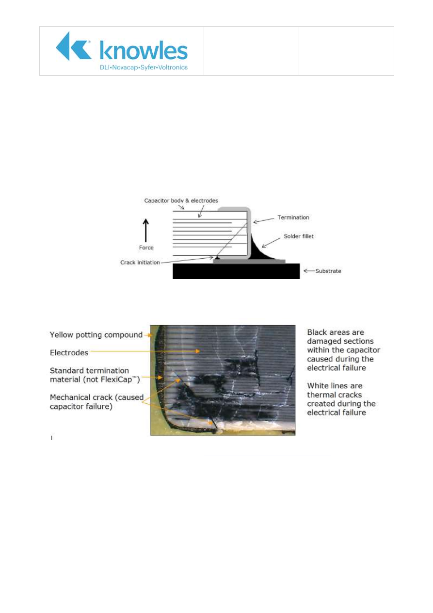
Application Note
Reference No: AN0008
Restricted Substances
Issue 4
Page 5 of 11
and the onset of fatigue fractures. Generally lead-free being better in the range –40°C to 100°C and
much poorer when tested over –55 °C to 125/160°C. Few of these tests reflect the increased stress
transferred to the actual components and also the risk of mechanically cracking due to PCB flexing as
result of the comparatively hard and strong solder joints.
Unsupported PCBs will also flex more at the higher soldering temperatures and may apply additional
stress, increasing the chance of mechanical cracking.
Syfer has undertaken a range of tests and generally would recommend the use of polymer termination
for case sizes greater than 1206 in order reduce the amount of stress transferred to the ceramic
capacitor itself.
Example of mechanical cracking
Example of capacitor issued by customers to Syfer for failure investigation:
Information is also available on Syfer’s web site
www.knowlescapacitors.com/syfer
Application Note
Reference No: AN0008
Restricted Substances
Issue 4
Page 6 of 11
Appendix 1 Low Value C0G
Generic Component Material Declaration (all percentages are approximate)
Standard Nickel Barrier Product
Material
Element
CAS Number Low Value C0G
Typical Component Composition
Ceramic
Ba
7440-39-3
%
60-75% Ceramic
Ti
7440-32-6
17.5 %
Nd
7440-00-8
%
Bi
7440-69-9
%
Pb
7440-92-1
%
Co
7440-48-4
0.3 %
Zn
7440-66-6
7.5 %
Si
7440-21-3
8 %
Al
7440-90-5
8 %
B
7440-42-8
3 %
Mg
7440-95-4
17.5 %
Mn
7440-96-5
%
Zr
7440-67-7
%
Sn
7440-31-5
%
Nb
7440-03-1
%
Other primarily O
38.2 %
Electrode
3-8% Electrode
Ag
7440-22-4
75 %
Pd
7440-05-3
25 %
Termination
17-30% Termination
Ag
7440-22-4
94 %
Pd
7440-05-3
%
Pb
7440-92-1
4 %
Bi
7440-69-9
%
Other Primarily O, B, Si
2 %
Plating
3-5% Plating
Ni
7440-02-0
31 %
Sn
7440-31-5
69 %

Application Note
Reference No: AN0008
Restricted Substances
Issue 4
Page 7 of 11
Appendix 2 Mid Value C0G
Generic Component Material Declaration (all percentages are approximate)
Standard Nickel Barrier Product
Material
Element
CAS Number Low Value C0G
Typical Component Composition
Ceramic
Ba
7440-39-3
15 %
70-85% Ceramic
Ti
7440-32-6
25 %
Nd
7440-00-8
25 %
Bi
7440-69-9
7.5 %
Pb
7440-92-1
1.5 %
Co
7440-48-4
0.3 %
Zn
7440-66-6
0.8 %
Si
7440-21-3
0.3 %
Al
7440-90-5
%
B
7440-42-8
0.5 %
Mg
7440-95-4
%
Mn
7440-96-5
0.1 %
Zr
7440-67-7
%
Sn
7440-31-5
%
Nb
7440-03-1
%
Other primarily O
24 %
Electrode
3-7% Electrode
Ag
7440-22-4
75 %
Pd
7440-05-3
25 %
Termination
8-20% Termination
Ag
7440-22-4
94 %
Pd
7440-05-3
%
Pb
7440-92-1
4 %
Bi
7440-69-9
%
Other Primarily O, B, Si
2 %
Plating
1-3% Plating
Ni
7440-02-0
31 %
Sn
7440-31-5
69 %

Application Note
Reference No: AN0008
Restricted Substances
Issue 4
Page 8 of 11
Appendix 3 High Value C0G
Generic Component Material Declaration (all percentages are approximate)
Standard Nickel Barrier Product
Material
Element
CAS Number Low Value C0G
Typical Component Composition
Ceramic
Ba
7440-39-3
15 %
65-80% Ceramic
Ti
7440-32-6
20 %
Nd
7440-00-8
25 %
Bi
7440-69-9
10 %
Pb
7440-92-1
3 %
Co
7440-48-4
%
Zn
7440-66-6
2 %
Si
7440-21-3
%
Al
7440-90-5
%
B
7440-42-8
%
Mg
7440-95-4
%
Mn
7440-96-5
%
Zr
7440-67-7
%
Sn
7440-31-5
2 %
Nb
7440-03-1
%
Other primarily O
23 %
Electrode
5-15% Electrode
Ag
7440-22-4
90 %
Pd
7440-05-3
10 %
Termination
5-17% Termination
Ag
7440-22-4
94 %
Pd
7440-05-3
%
Pb
7440-92-1
4 %
Bi
7440-69-9
%
Other Primarily O, B, Si
2 %
Plating
1-3% Plating
Ni
7440-02-0
31 %
Sn
7440-31-5
69 %

Application Note
Reference No: AN0008
Restricted Substances
Issue 4
Page 9 of 11
Appendix 4 Low Value X7R
Generic Component Material Declaration (all percentages are approximate)
Standard Nickel Barrier Product
Material
Element
CAS Number Low Value C0G
Typical Component Composition
Ceramic
Ba
7440-39-3
55 %
75-90% Ceramic
Ti
7440-32-6
15 %
Nd
7440-00-8
%
Bi
7440-69-9
2 %
Pb
7440-92-1
1.5 %
Co
7440-48-4
0.3 %
Zn
7440-66-6
0.8 %
Si
7440-21-3
%
Al
7440-90-5
%
B
7440-42-8
0.5 %
Mg
7440-95-4
%
Mn
7440-96-5
%
Zr
7440-67-7
%
Sn
7440-31-5
%
Nb
7440-03-1
%
Other primarily O
24.9 %
Electrode
1-5% Electrode
Ag
7440-22-4
75 %
Pd
7440-05-3
25 %
Termination
5-17% Termination
Ag
7440-22-4
94 %
Pd
7440-05-3
%
Pb
7440-92-1
4 %
Bi
7440-69-9
%
Other Primarily O, B, Si
2 %
Plating
1-3% Plating
Ni
7440-02-0
31 %
Sn
7440-31-5
69 %

Application Note
Reference No: AN0008
Restricted Substances
Issue 4
Page 10 of 11
Appendix 5 Mid Value X7R
Generic Component Material Declaration (all percentages are approximate)
Standard Nickel Barrier Product
Material
Element
CAS Number Low Value C0G
Typical Component Composition
Ceramic
Ba
7440-39-3
58 %
70-85% Ceramic
Ti
7440-32-6
20 %
Nd
7440-00-8
0.8 %
Bi
7440-69-9
0.4 %
Pb
7440-92-1
%
Co
7440-48-4
%
Zn
7440-66-6
0.5 %
Si
7440-21-3
%
Al
7440-90-5
%
B
7440-42-8
%
Mg
7440-95-4
%
Mn
7440-96-5
%
Zr
7440-67-7
%
Sn
7440-31-5
%
Nb
7440-03-1
0.5 %
Other primarily O
19.8 %
Electrode
3-10% Electrode
Ag
7440-22-4
85 %
Pd
7440-05-3
15 %
Termination
8-20% Termination
Ag
7440-22-4
94 %
Pd
7440-05-3
%
Pb
7440-92-1
4 %
Bi
7440-69-9
%
Other Primarily O, B, Si
2 %
Plating
1-3% Plating
Ni
7440-02-0
31 %
Sn
7440-31-5
69 %

Application Note
Reference No: AN0008
Restricted Substances
Issue 4
Page 11 of 11
Appendix 6 High value X7R
Generic Component Material Declaration (all percentages are approximate)
Standard Nickel Barrier Product
Material
Element
CAS Number Low Value C0G
Typical Component Composition
Ceramic
Ba
7440-39-3
58 %
65-80% Ceramic
Ti
7440-32-6
20 %
Nd
7440-00-8
0.8 %
Bi
7440-69-9
%
Pb
7440-92-1
%
Co
7440-48-4
%
Zn
7440-66-6
0.5 %
Si
7440-21-3
%
Al
7440-90-5
%
B
7440-42-8
%
Mg
7440-95-4
%
Mn
7440-96-5
%
Zr
7440-67-7
%
Sn
7440-31-5
%
Nb
7440-03-1
0.5 %
Other primarily O
20.2 %
Electrode
5-15% Electrode
Ag
7440-22-4
70 %
Pd
7440-05-3
30 %
Termination
5-17% Termination
Ag
7440-22-4
94 %
Pd
7440-05-3
%
Pb
7440-92-1
4 %
Bi
7440-69-9
%
Other Primarily O, B, Si
2 %
Plating
1-3% Plating
Ni
7440-02-0
31 %
Sn
7440-31-5
69 %

AN0009 Issue 11 – AEC-Q200 Stress Test
CN# P109825
Automotive Electronics Council-Q200
Stress Test Qualification for Passive
Components
Syfer AEC-Q200-Rev C Qualification
Syfer Product Reliability Guide
AEC-Q200 Stress-Test Qualification
AEC-Q200 Temperature Range Grades
AEC-Q200 Stress Test Qualification Requirements
Batch Tests (Standard & Optional Tests Available)
AEC-Q200 Qualified Component Ranges
Knowles (UK) Limited,
Old Stoke Road, Arminghall, Norwich,
Norfolk, NR14 8SQ, United Kingdom
Tel: +44 (0) 1603 723300
Tel. (Sales): 01603 723310
Fax: +44 (0) 1603 723301
www.knowlescapacitors.com/syfer
Application Note
Reference No: AN0009
AEC-Q200 Stress Test
Issue 11
Page 2 of 7
Introduction
The Automotive Electronics Council (AEC) Component Technical Committee is the standardization body
for establishing standards for reliable, high quality electronic components. Components meeting these
specifications are suitable for use in the harsh automotive environment without additional component-
level qualification testing.
The Component Technical Committee established AEC-Q200 “Stress Test Qualification for Passive
Components” to define the minimum stress test driven qualification requirements for passive electrical
devices including ceramic capacitors.
This application note provides information on tests performed by Syfer in accordance with the AEC-
Q200 specification.
For further information regarding the Automotive Electronics Council and AEC-Q200, refer to website
Note: Supply of AEC-Q200 qualified components is not limited to the automotive industry. Other
industries are also recognising the benefits of AEC-Q200 qualified components.
Syfer Product Reliability Guide
Notes:
(1) Space Grade tested in accordance with ESCC 3009. Refer to Syfer specification S02A 0100.
(2)
IECQ-CECC. The International Electrotechnical Commission (IEC) Quality Assessment System for
Electronic Components. This is an internationally recognised product quality certification. View
Syfer’s IECQ-CECC approvals at
or at
www.knowlescapacitors.com/syfer
(3) AEC-Q200. Automotive Electronics Council Stress Test Qualification For Passive Components.
(4) MIL Grade. Released in accordance with US MIL standards available on request.
Space
Grade
IECQ-CECC
(2)
AEC-Q200
(3)
MIL Grade
(4
)
Standard Components
ESCC 3009
(1)
High Reliability
(Space Quality)
Standard Reliability
Application Note
Reference No: AN0009
AEC-Q200 Stress Test
Issue 11
Page 3 of 7
AEC-Q200 Stress-Test Qualification
Qualification is defined as successful completion of the test requirements defined in AEC-Q200.
Approval is defined as user approval for use of the component within the customer’s application and,
as such, is beyond the scope of AEC-Q200.
AEC-Q200 Temperature Range Grades
Temperature range grades defined in AEC-Q200:
Grade
Temperature Range
PASSIVE COMPONENT TYPE
Maximum capability
TYPICAL/ EXAMPLE
APPLICATION
MINIMUM MAXIMUM
0
-50ºC
+150 ºC
Flat chip ceramic resistors, X8R
ceramic capacitors
All automotive
1
-40ºC
+125 ºC
Capacitor Networks, Resistors,
Inductors, Transformers,
Thermistors, Resonators,
Crystals and Varistors, all other
ceramic and tantalum capacitors
Most underhood
2
-40ºC
+105 ºC
Aluminium Electrolytic capacitors Passenger compartment
hot spots
3
-40ºC
+85 ºC
Film capacitors, Ferrites, R/R-C
Networks and Trimmer
capacitors
Most passenger
compartment
4
0ºC
+70 ºC
Non-automotive
Syfer AEC-Q200 qualified components are rated from -55 ºC to +125 ºC. Corresponding AEC-Q200
qualified grades are 1, 2, 3 and 4.
Qualification Families
Syfer AEC-Q200 qualification has been conducted in accordance with AEC-Q200 qualification family
guidelines. AEC-Q200 defines a qualification family as a group of components that share the same
major process and material elements. All components categorized in the same family are qualified by
association when one family member successfully completes qualification.
Qualification test summary is available on request.
Application Note
Reference No: AN0009
AEC-Q200 Stress Test
Issue 11
Page 4 of 7
AEC-Q200 Stress Test Qualification Requirements
Stress
Test #
Test Method
Sample size per
lot
Accept on
number failed
Additional Requirements
Pre- and Post Stress
Electrical Test
1
User Spec.
All qualification parts
submitted for testing
0
Test Not Used
2
-
-
-
-
High Temperature
Exposure (Storage)
3
MIL-STD-202 Method
108
77
0
Unpowered
1000 hours @ 150ºC
Temperature Cycling
4
JESD22 Method JA-104
77
0
1000 cycles (-55ºC to 125ºC)
Destructive Physical
Analysis
5
EIA-469
10
0
10ea x 3 lots
Moisture Resistance
6
MIL-STD-202 Method
106
77
0
t = 24 hours/cycle. Unpowered.
Biased Humidity
7
MIL-STD-202 Method
103
77
0
1000 hrs 85ºC/ 85%RH. 1.5Vdc
and Rated Voltage
(1)
Operational Life
8
MIL-STD-202 Method
108
77
0
Rated Voltage @ 125ºC
External Visual
9
MIL-STD-883 Method
2009
All qualification parts
submitted for testing
0
Inspect device construction and
workmanship. Electrical test not
required.
Physical Dimension
10
JESD22 Method JB-100
30
0
Verify physical dimensions to the
device specification
Terminal Strength
(Leaded)
11
Not applicable for
surface mount
capacitors
-
-
-
Resistance to Solvents
12
MIL-STD-202 Method
215
5
0
Note: Add Aqueous wash
chemical – OKEM or equivalent.
No banned substances.
Mechanical Shock
13
MIL-STD-202 Method
213
30
0
Figure 1 of Method 213 SMD:
Condition F.
Vibration
14
MIL-STD-202 Method
204
5 g’s for 20 min., 12 cycles each
of 3 orientations. Test from 10-
2000Hz.
Resistance to Soldering
Heat
15
MIL-STD-202 Method
210
30
0
Condition B No pre-heat of
samples.
Thermal Shock
16
MIL-STD-202 Method
107
30
0
-55ºC/+125ºC. 300 cycles. Max
transfer time: 20s. Dwell time:
15minutes. Air-Air.
ESD
17
AEC-Q200-002
15
0
Solderability
18
J-STD-002 (JESD22-
B102
(2)
)
15 each condition
0
Electrical
Characterization
19
User specification
30
0
Parametrically test per lot at
room temp & min, max temps
Test not used
20
-
-
-
-
Board flex
21
AEC-Q200-005
30
0
2mm (min) for all except 3mm
for Class 1.
Terminal strength
22
AEC-Q200-006
30
0
Force of 1.8kg for 60s.
Beam Load Test
23
AEC-Q200-003
30
0
Notes:
1 Biased Humidity test conducted by Syfer with rated voltage or 200Vdc (whichever is the least) applied.
2 JESD22-B102 150°C dry bake preconditioning applied.
Table 1 – Stress Test Qualification Requirements
Application Note
Reference No: AN0009
AEC-Q200 Stress Test
Issue 11
Page 5 of 7
Batch Tests (Standard & Optional Tests Available)
Test
Standard
tests
Test
Optional
tests
Solderability
●
100% Burn-In. (2xRV @125º
for 168hours).
○
Resistance to soldering
heat
●
Load sample test @ 125ºC
○
Plating thickness
verification (if plated)
●
Humidity sample test.
85 ºC/85%RH
○
DPA (Destructive Physical
Analysis)
●
Hot IR sample test
○
Voltage Proof Test (DWV
& Flash)
●
Axial Pull sample test (MIL-
STD-123)
○
Insulation Resistance
●
Breakdown Voltage sample
test
○
Capacitance Test
●
Deflection (Bend) sample test
○
Dissipation Factor Test
●
SAM (Scanning Acoustic
Microscopy)
○
100% Visual Inspection
●
For further details, optional test quotations please contact Syfer Sales department.
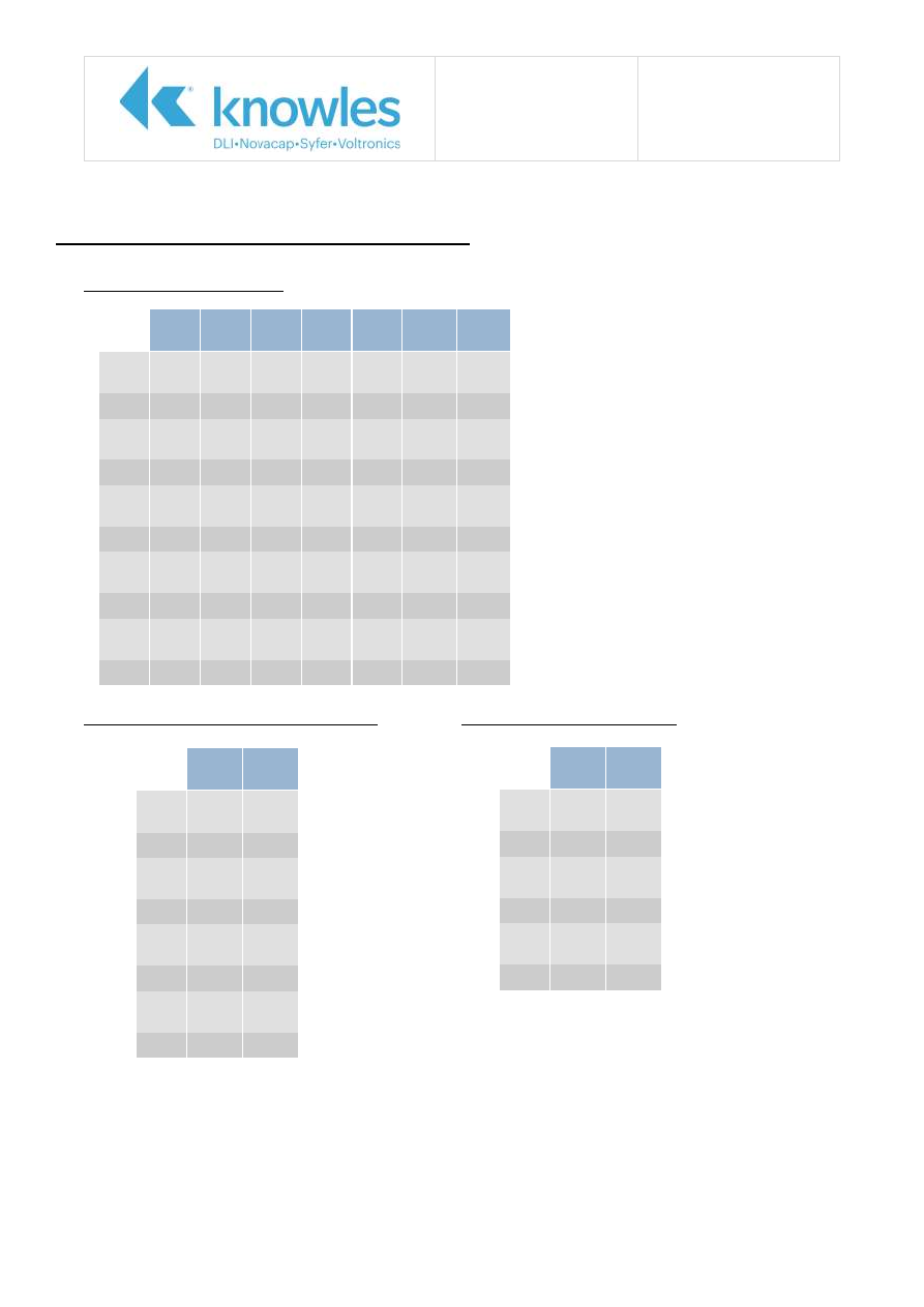
Application Note
Reference No: AN0009
AEC-Q200 Stress Test
Issue 11
Page 6 of 7
AEC-Q200 Qualified Component Ranges
Surface Mount Capacitors
Balanced Line EMI Chip Ranges (E03)
3 Terminal EMI Chips (E01)
Max
Cap
50V 63V 100V 200V 500V 630V 1.0KV
C0G/
NP0
470pF 470pF 330pF 100pF n/a
n/a
n/a
0603
X7R
33nF 33nF 10nF 5.6nF n/a
n/a
n/a
C0G/
NP0
2.7nF 2.7nF 1.8nF 680pF 330pF
n/a
n/a
0805
X7R
150nF 150nF 47nF 27nF 8.2nF
n/a
n/a
C0G/
NP0
10nF 10nF 6.8nF 2.2nF 1.5nF
1nF
470pF
1206
X7R
330nF 330nF 150nF 100nF 33nF 10nF 4.7nF
C0G/
NP0
18nF 18nF 12nF 4.7nF 3.9nF 1.8nF
1nF
1210
X7R
680nF 680nF 470nF 220nF 100nF 27nF
15nF
C0G/
NP0
39nF 39nF 27nF 12nF 10nF 5.6nF 3.3nF
1812
X7R
1.5µF 1.5µF 1µF 470nF 270nF 150nF 56nF
Max
Cap
50V 100V
C0G/
NP0
470pF 330pF
0805
X7R
33nF
15nF
C0G/
NP0
1.5nF
1nF
1206
X7R
150nF 47nF
C0G/
NP0
5.6nF 3.9nF
1410
X7R
330nF 150nF
C0G/
NP0
10nF 6.8nF
1812
X7R
560nF 330nF
Max
Cap
50V 100V
C0G/
NP0
820pF 560pF
0805
X7R
47nF
15nF
C0G/
NP0
1.0nF 1.0nF
1206
X7R
100nF 15nF
C0G/
NP0
2.2nF 2.2nF
1806
X7R
200nF 68nF

Application Note
Reference No: AN0009
AEC-Q200 Stress Test
Issue 11
Page 7 of 7
Ordering Information
Part Number Construction:
1210
Y
100
0103
J
E
T
_ _ _
Chip Size
Termination
Rated Voltage
Capacitance in Pico
farads (pF)
Capacitance
Tolerance
Dielectric
Codes
Packaging
Suffix code
0603
0805
1206
1210
1812
Y
= FlexiCap™
termination base with
nickel barrier (100%
matte tin plating).
RoHS compliant.
H
= FlexiCap™
termination base with
nickel barrier (Tin/
lead plating with min.
10% lead). Not RoHS
compliant.
J
= Silver base with
nickel barrier (100%
matte tin plating).
RoHS compliant.
A
= Silver base with
nickel barrier (Tin/lead
plating with min. 10%
lead). Not RoHS
compliant. Available in
C0G/NP0 only.
050
= 50V
063
= 63V
100
= 100V
200
= 200V
250
= 250V
500
= 500V
630
= 630V
1K0
= 1kV
First digit is 0.
Second and third digits are
significant figures of
capacitance code. The fourth
digit is number of zeros
following. Example:
0103
= 10nF
<10pF
B
= ±0.1pF
C
= ±0.25pF
D
= ±0.5pF
≥ 10pF
F
= ±1%
G
= ±2%
J
= ±5%
K
= ±10%
M
= ±20%
E
= X7R (2R1)
AEC-Q200
A
= C0G/NP0
(1B/NP0) AEC-Q200
T
= 178mm
(7”) reel
R
= 330mm
(13”) reel
B
= Bulk pack
- tubs or trays
Used for specific
customer
requirements
For questions or quotation please contact Syfer Sales department.

AN0010 Issue 5 – Lead Free Bend Test Performance
CN# P109825
The Effect of Lead Free Soldering on
Bend Test Performance
Methods and International Specifications
International Requirements/ Specifications ..................................................2
Capacitor Bend Tests Conducted on Syfer Product ........................................3
Mechanical Crack Shape ............................................................................6
The Effect of Lead Free Solders on Mechanical Cracking of MLCC’s ..................7
Lead Free Bend Test Conclusion .................................................................8
Knowles (UK) Limited,
Old Stoke Road, Arminghall, Norwich,
Norfolk, NR14 8SQ, United Kingdom
Tel: +44 (0) 1603 723300
Tel. (Sales): 01603 723310
Fax: +44 (0) 1603 723301
www.knowlescapacitors.com/syfer

Application Note
Reference No: AN0010
Lead Free Bend Test
Performance
Issue 5
Page 2 of 8
Introduction
Due to its brittle nature, multilayer ceramic capacitors are more prone to excesses of mechanical stress
than other components used in surface mounting. One of the most common causes of capacitor
failures is directly attributable to the bending of the printed circuit board (PCB) after solder
attachment. Excessive bending will create mechanical stress within the ceramic capacitor that, if
sufficient, can result in mechanical cracks.
The introduction of lead free solders for attachment of chip capacitors to PCB’s has raised a further
area of concern in that lead free solders are less ductile than their traditional tin/lead equivalents. This
raises the possibility that the lead free solders demanded by the EU RoHS directive could cause an
increase in the incidences of chip failure due to mechanical cracking as stress is transferred to the chip
rather than absorbed by the solder.
The purpose of this report is to provide details regarding:
a.
For background information, methods employed by Syfer to measure the mechanical
performance of the termination material.
b.
For background information, the shape of cracks created by PCB bending - mechanical stress.
c.
Testing carried out by Syfer to determine the effects of lead free solders on the mean bend
performance of ceramic chip capacitors.
International Requirements/ Specifications
The international requirement for bend testing is referred to in several different specifications.
1.
section 4.35 Substrate bending test refers to IEC 60068-2-21.
2.
IEC 60068-2-21: 1999 Environmental testing: Test U: Robustness of Terminations and Integral
Mounting Devices. Section 8 test Ue specifies the test required to assess the mechanical
robustness of surface mounting device terminations when mounted on a substrate. Test Ue
1
specifies the substrate bend test.
The purpose of test Ue
1
is to verify that the capacitors can withstand bending loads that are likely
to be applied during normal assembly or handling operations.
IEC 60068-2-21 refers to requirements such as deflection and acceptance criteria as being
included in the “relevant specification”. Syfer maintains IECQ CECC (International Electrotechnical
Commission Quality certification programme- CENELEC Electronic Components Committee)
product approval and the “relevant specification” is QC 32100-A001:2007.
3.
QC 32100-A001:2007 Table 2 – Periodic Tests defines board flex minimum requirements as:
COG: All types, X7R: Y and H only (Flexicap™)
3mm deflection Class I.
2mm deflection Class II.
X7R (non – Flexicap™ termination) 1mm deflection.
4.
AEC-Q200-005, Board Flex / Terminal Bond Strength Test.
Minimum requirements stated in table 2 stress test reference 21: 2mm (min) for all except 3mm for
Class I.
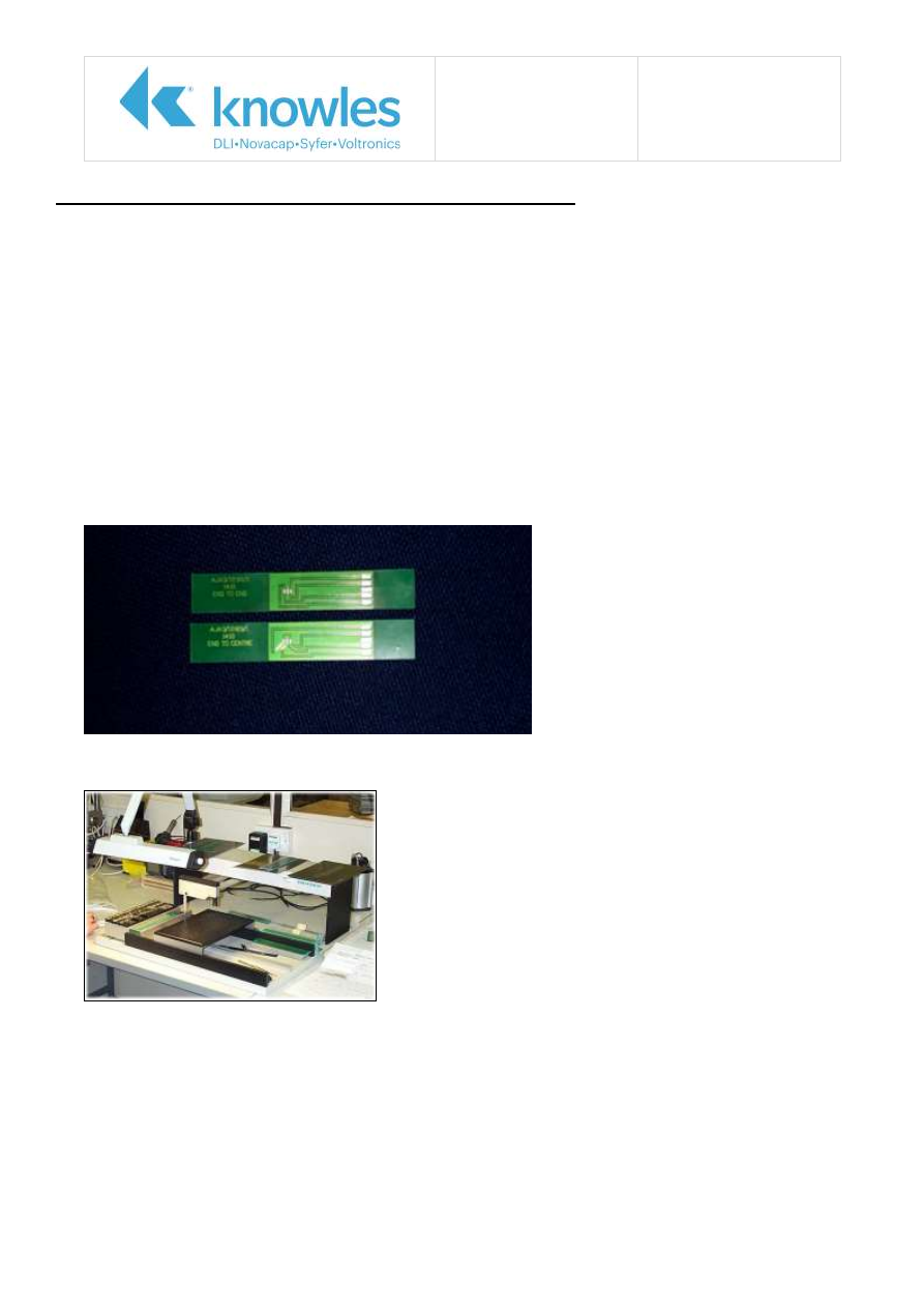
Application Note
Reference No: AN0010
Lead Free Bend Test
Performance
Issue 5
Page 3 of 8
Capacitor Bend Tests Conducted on Syfer Product
Currently there are 2 methods employed by Syfer to measure the mechanical performance of capacitor
termination when mounted on a substrate:
1.
External Test Laboratory
To maintain IECQ CECC product approval (certified by BSI “British Standards Institute”) Syfer
issues capacitor samples to an external test laboratory for a variety of tests to be conducted in
accordance with IECQ CECC requirements. The external test laboratory is not part of Syfer and
has full traceability to International Reference Standards.
Syfer has maintained CECC product approval for >20 years.
2. Syfer Bend Tests
In addition to the external test laboratory Syfer also conducts bend tests. Samples of capacitors
are mounted onto FR4 Test PCBs using 62/36/2 Sn/Pb/Ag solder and subjected to bend testing in
accordance with IECQ CECC or AEC –Q200-005 (depending on termination and dielectric types.
Capacitor Placement Method
Hand pick and place used to
mount capacitors for bend tests
Example of FR4
Test PCB Used
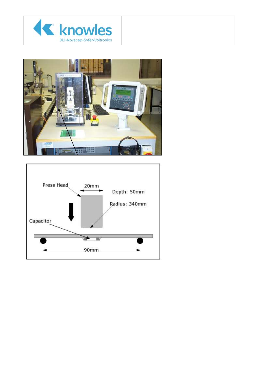
Application Note
Reference No: AN0010
Lead Free Bend Test
Performance
Issue 5
Page 4 of 8
Syfer’s Bend Test Facility
Fig 1. Bend Test Method
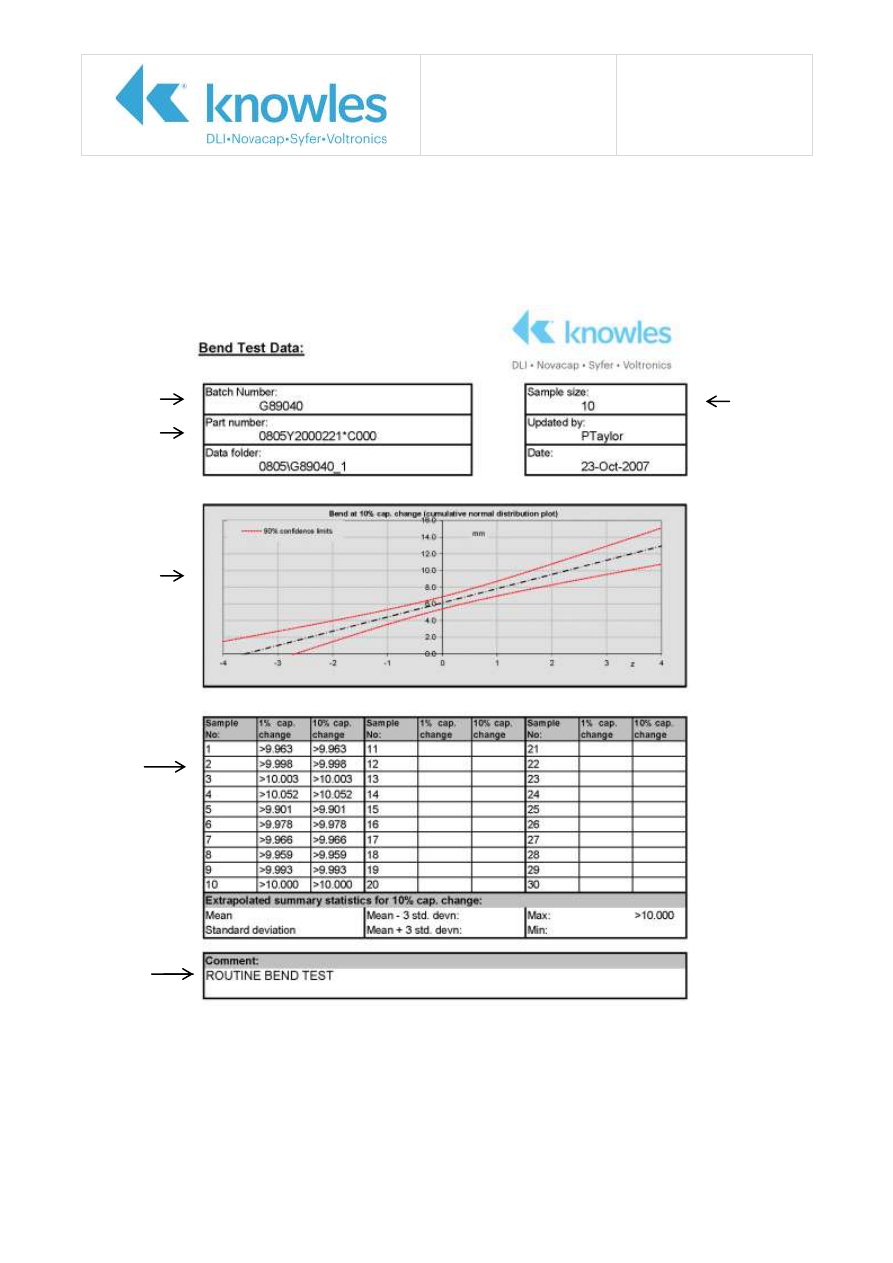
Application Note
Reference No: AN0010
Lead Free Bend Test
Performance
Issue 5
Page 5 of 8
A total of 10 Test PCBs are used for each bend test. Each PCB is mounted with one capacitor and
deflected automatically until the capacitor breaks. The software analyses the change in capacitance
measured by the Agilent 4288A capacitance meter. As soon as the capacitance change is greater than
10% the bend is recorded in mm.
The results of the test are saved to the Syfer network but also can be communicated as a printed
document as below.
Document shows the results for Flexicap™ terminated components.
Syfer Batch No:
Syfer Part No:
Distribution
Plot
Sample Size
Measured
Results
Type of Test
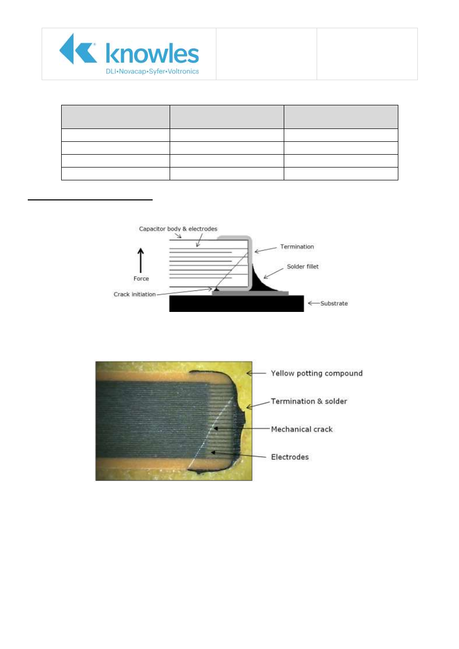
Application Note
Reference No: AN0010
Lead Free Bend Test
Performance
Issue 5
Page 6 of 8
Typical results for Syfer X7R 0805, 1206, 1812 and 2220 capacitor ranges:
Product
Mean Bend (mm)
Sintered Termination
Mean Bend (mm)
Flexicap™
Termination
0805 X7R
3.6
6.3
1206 X7R
3.4
6.4
1812 X7R
3.2
6.0
2220 X7R
3.2
6.1
Mechanical Crack Shape
By conducting extensive bend testing capacitor manufacturers including Syfer have demonstrated that
mechanical stress applied by bending the PCB results in a distinctive type of crack within the capacitor.
During Syfer’s initial investigation into mechanical cracking over 15000 capacitors were subjected to bend
testing.
Example of capacitors issued by customers to Syfer for failure investigation:
Summary
Syfer capacitors pass the International Specifications for bend testing. In addition to routine
tests conducted at Syfer an external test laboratory conducts periodic CECC tests on Syfer
product including bend testing.
The crack created by mechanical stress during PCB bending is a distinctive type of crack.
For further information regarding:
Potential causes for mechanical cracking refer to Syfer application note AN0005 - Mechanical Cracking.
An alternative termination material that withstands higher levels of mechanical stress refer to Syfer application
note AN0001 – FlexiCap™ Termination.

Application Note
Reference No: AN0010
Lead Free Bend Test
Performance
Issue 5
Page 7 of 8
The Effect of Lead Free Solders on Mechanical Cracking of MLCC’s
As mentioned above, one concern with lead free solders is that the reduced ductility in the solder could
lead to increased incidences of mechanical cracking of the ceramic.
To ascertain if this concern was real, Syfer instigated a test program to compare the bend test results
of a number of 1206 size X7R chip capacitors when soldered with conventional tin/lead (Sn/Pb) solders
and with a common lead free solder alloy - 95.5/3.8/0.7 SnAgCu (SAC). Both conventional ‘J’ chip
termination (plated tin over nickel over Silver/glass termination material) and Syfer ‘Y’ FlexiCap™
(plated tin over nickel over flexible Silver polymer termination material) were tested and ageing at
ambient temperature was taken into account to evaluate if the subtle changes in solder particle size
over time had any effect.
Testing Carried Out
Mount 80 capacitors of each of 5 types of conventionally terminated capacitors to boards using
60/40 SnPb solder and carry out bend testing as above.
Mount 80 capacitors of each of 5 types of FlexiCap™ terminated capacitors to boards using
60/40 SnPb solder and carry out bend testing as above.
Mount 80 capacitors of each of 5 types of conventionally terminated capacitors to boards using
95.5/3.8/0.7 SAC solder and carry out bend testing as above.
Mount 80 capacitors of each of 5 types of FlexiCap™ terminated capacitors to boards using
95.5/3.8/0.7 SAC solder and carry out bend testing as above.
Mount 80 capacitors of each of 5 types of conventionally terminated capacitors to boards using
SAC solder, allow to age for 1000hrs at ambient temperature and carry out bend testing as
above.
Mount 80 capacitors of each of 5 types of FlexiCap™ terminated capacitors to boards using SAC
solder, allow to age for 1000hrs at ambient temperature and carry out bend testing as above.
Total number of capacitors tested = 2400.
Where conventional SnPb solder was used, board finish was Hot Air Solder Levelled (HASL). Where Pb
free solder (SAC) was used, board finish was gold (Au) flash over nickel (Ni) plate (NIG).
All boards were assembled using hot air reflow methods. Peak solder temperatures were 220ºC for
SnPb and 260ºC for SAC solder. In both cases, parts were allowed to cool naturally to ambient
temperature – forced cooling was not used as this can itself induce cracks in the ceramic giving false
results.
Application Note
Reference No: AN0010
Lead Free Bend Test
Performance
Issue 5
Page 8 of 8
Results
For each set of tests, the results, consisting of the number of fractures and capacitance failures at each
bend distance, are entered into a database and the mean bend distance is calculated.
These mean bends can then be compared to evaluate the effect of the two different solders.
Chip
Size
Termination
Mean Bend
SnPb Solder
(mm)
Mean Bend
SnAgCu
Solder
(mm)
Difference in
mean bend
between
conventional and
Pb free solders
1206
‘J’ Termination
3.4
3.2
- 0.2mm
‘Y’ FlexiCap™
6.7
6.5
- 0.2mm
After ageing for 1000hrs:
Chip
Size
Termination
Mean Bend SnAgCu
Solder
0hrs @ 25ºC
(mm)
Mean Bend SnAgCu
Solder
1000hrs @ 25ºC
(mm)
1206
‘J’ Termination
3.2
3.5
‘Y’ FlexiCap™
6.5
6.7
As solder ages it will change its internal grain structure, which can change the effect it has on the
ceramic during bending. The results above show that the mean bend angle does change with
prolonged storage and that after 1000hrs at ambient the two types of solder tend towards the same
result.
Lead Free Bend Test Conclusion
Soldering with lead free solders marginally reduces the mean bend performance of multilayer chip
capacitors mounted on a circuit board.
This change is small, and provided the normal recommendations are observed is unlikely to cause any
significant problem within a lead free process. However, where an existing process is ‘on the edge’ the
change to lead free may be sufficient to cause processing problems.
Given time, the grain structure within the solder joint will age to a similar structure to that of lead
containing solders and the mean bends for both solders will be very similar.
Although Syfer’s FlexiCap™ showed a similar marginal decline in performance when soldered with lead
free, in all tests it continued to significantly outperform the conventional termination and is therefore
the preferred choice for lead free soldering.
Further information on FlexiCap™ is available on Syfer’s web site

AN0011 Issue 8 – Solder Alloy Choice
CN# P109825
Solder Alloy Choice for Through Hole
Ceramic Discoidal & Planar Array
Capacitors
Introduction to through hole ceramic capacitors ...........................................3
Investigation into cause of cracks ...............................................................7
1) Solder Type 62Sn/36Pb/2Ag ..................................................................9
2) Solder Type 60Sn/40Pb.........................................................................10
3) Solder Type 99.3Sn/0.7Cu ....................................................................11
4) Solder Type 95.5Sn/3.8Ag/0.7Cu ...........................................................12
5) Solder Type 50In / 50Pb .......................................................................13
7) Solder Type 93.5Pb/5Sn/1.5Ag ..............................................................15
Demonstration of effect with PdAg termination ............................................17
Testing PdAg termination and Pb free solder alloy ........................................18
Analysis of the differences between gold plate and PdAg terminations ............22
Comments on fritted termination in discoidal and planar capacitors ................24
Knowles (UK) Limited,
Old Stoke Road, Arminghall, Norwich,
Norfolk, NR14 8SQ, United Kingdom
Tel: +44 (0) 1603 723300
Tel. (Sales): 01603 723310
Fax: +44 (0) 1603 723301
www.knowlescapacitors.com/syfer

Application Note
Reference No: AN0011
Solder Alloy Choice for
Through Hole Ceramic
Discoidal & Planar Array
Capacitors Issue 8
Page 2 of 26
Introduction
It has been well known for a number of years that solder alloy choice is a critical factor in soldering
to ceramic discoidal and planar array capacitors. The introduction of lead free solder alloys as a
result of the EU ‘RoHS’ directive and other similar directives around the world has prompted further
investigation into this phenomenon to categorise the effects of these alloys.
This application note aims to demonstrate the effect the choice of solder alloy has when soldering
to the internal bore of these through hole capacitors.
Application Note
Reference No: AN0011
Solder Alloy Choice for
Through Hole Ceramic
Discoidal & Planar Array
Capacitors Issue 8
Page 3 of 26
Introduction to through hole ceramic capacitors
Through hole ceramic capacitors are based on the technology of multi layer chip capacitors (MLCC’s)
with modified internal architecture. The manufacture is similar to MLCC’s in that layers of ceramic
dielectric material interlaced with precious metal electrodes are built up to form the structure, but
holes are then drilled in the ceramic to form contacts to the inner or hot electrodes. The outside is
machined to shape and makes contact to the outer or cold electrodes. The capacitance is formed
between the hole and the outside edge. In the case of planar arrays, capacitance is formed between
each hole and the outside edge. Within limits, each hole can have different capacitance characteristics.
Single hole devices are usually referred to as discs (they are not necessarily circular) whilst multi hole
devices are referred to as planar arrays.
The materials involved are typically BaTiO
3
ceramic dielectric with PdAg electrodes. Terminations are
usually plated Au over Ni directly onto the ceramic surface, or sometimes PdAg based fritted glass
solderable terminations.
The finished capacitor device is used in the assembly of EMI filters and filter assemblies. Their special
construction allows the devices to have superior high frequency performance to SM chip based filtering
– important for applications such as military, aeronautical and medical. For the construction of an EMI
filter, the discoidal or array is soldered into a carrying can, or body, with a pin soldered through the
centre. The assembly can then be encapsulated to give improved mechanical and environmental
protection. The signal to be filtered is passed through the pin and the outside of the body connected to
earth.
The pin and body are usually manufactured from Cu or Cu based alloys, plated with Ag or Au.
Fig 2
Examples of Discoidal and
Planar Array Capacitors
Fig 1
Typical Discoidal
Construction
Internal electrode Structure
Metallised or
plated termination
area
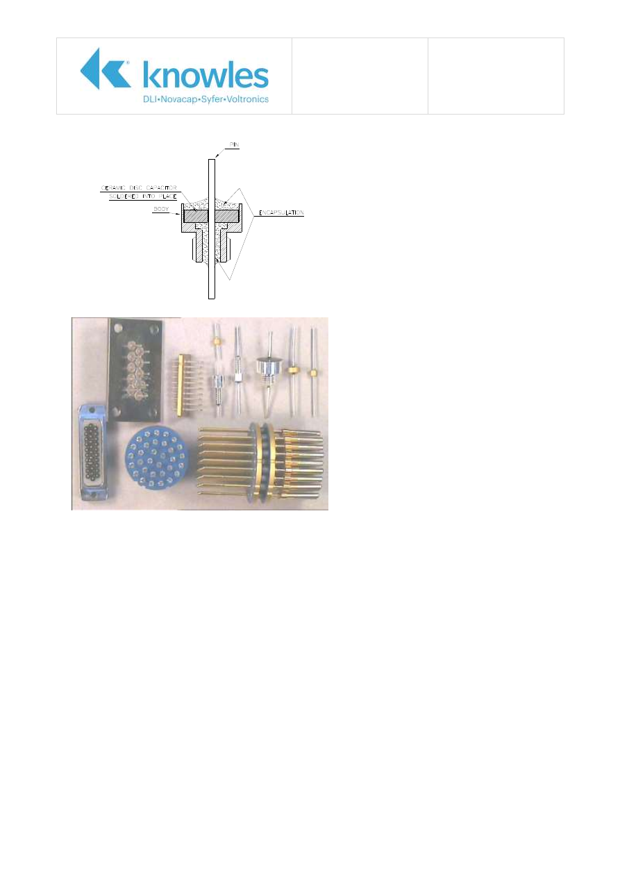
Application Note
Reference No: AN0011
Solder Alloy Choice for
Through Hole Ceramic
Discoidal & Planar Array
Capacitors Issue 8
Page 4 of 26
Fig 3
Typical Emi Filter
Construction
Fig 4
Examples of Emi Filters and
Assemblies
Application Note
Reference No: AN0011
Solder Alloy Choice for
Through Hole Ceramic
Discoidal & Planar Array
Capacitors Issue 8
Page 5 of 26
General soldering trials
It has been acknowledged for some years that soldering to the internal bore of the capacitor had the
potential to induce cracks within the ceramic structure. The cracks generated by this process are
known as ‘Longbow’ or ‘Comma’ cracks from their distinctive shape when viewed from a side cross
section or top cross section respectively.
These cracks can be benign or can cause total electrical failure, dependant on whether they pass
through the area of electrode overlap. Possibly of more concern, the cracks can be instigated during
soldering, but only propagate during further processing or in use, whereupon the capacitor can fail in
operation.
Capacitor failure will always tend towards a short circuit. If there is sufficient electrical power
available, the part will then become extremely hot and can represent a source of combustion.
A further form of crack commonly found in through hole ceramic capacitors is the corner crack. This
occurs when the solder fillet on the surface pad shrinks causing the ceramic to crack and lift. It can be
likened to the effect of pad lift on a circuit board.
Fig 5
‘Longbow Crack’
Capacitor soldered using
62Sn/36Pb/2Ag solder. Crack in
dielectric material generated
during cooling of solder joint
after reflow.
CERAMIC CAPACITOR
COPPER ALLOY PIN
SOLDER JOINT
CRACKS
Fig 6
‘Comma Crack’
The same crack as in Fig 3
above, but sectioned through a
plane 90º displaced.
COPPER ALLOY PIN
SOLDER JOINT
CRACKS
CERAMIC CAPACITOR
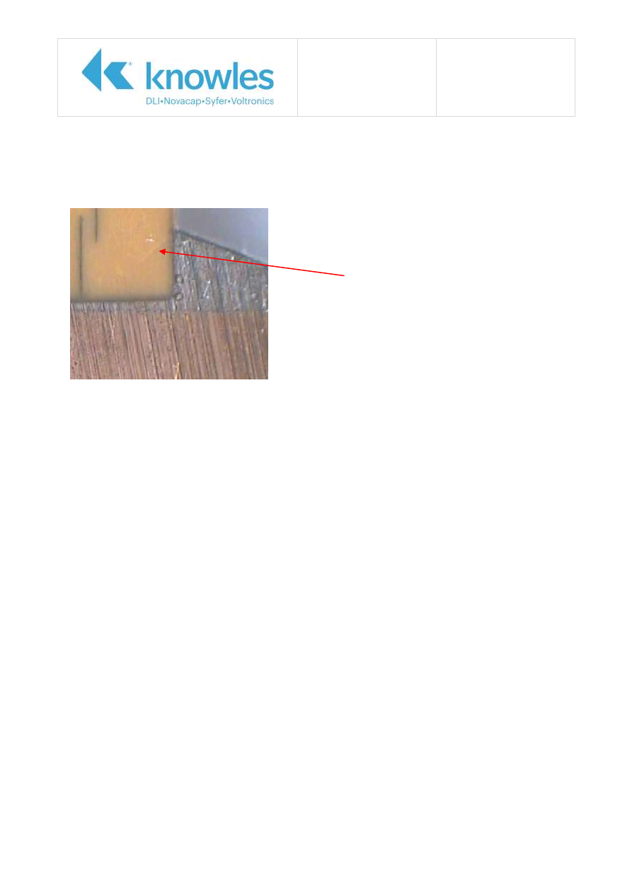
Application Note
Reference No: AN0011
Solder Alloy Choice for
Through Hole Ceramic
Discoidal & Planar Array
Capacitors Issue 8
Page 6 of 26
Corner cracking is less critical than longbow / comma cracking and rarely threatens immediate outright
dielectric failure, although the induced crack can propagate in operation causing failures. It can be
eased by limiting the volume of solder in the meniscus or reducing the pad size. On very small size
parts, it is common to remove the pad entirely.
Fig 7
‘Corner Crack’
Crack generated by lifting of the
pad due to the solder meniscus
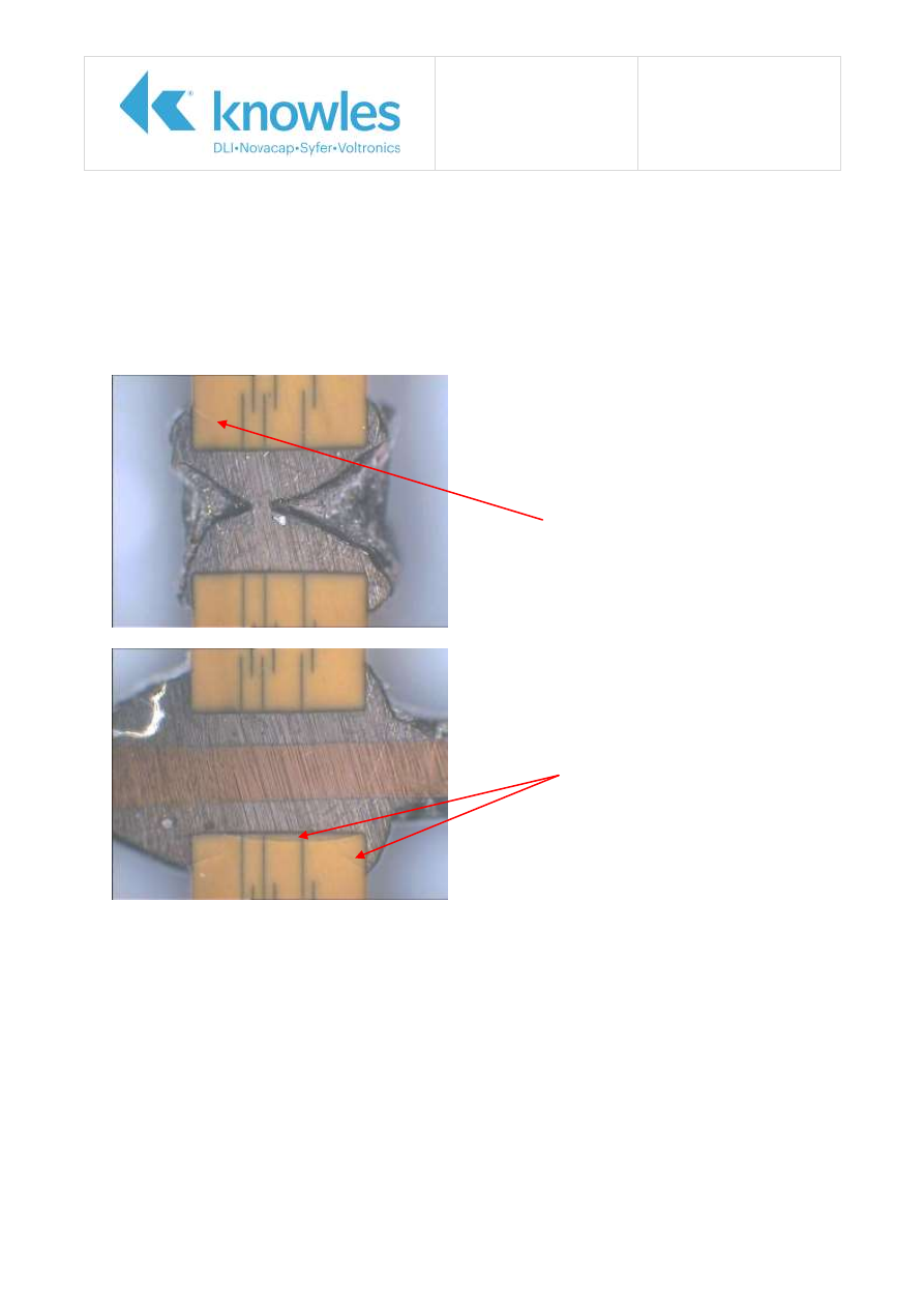
Application Note
Reference No: AN0011
Solder Alloy Choice for
Through Hole Ceramic
Discoidal & Planar Array
Capacitors Issue 8
Page 7 of 26
Investigation into cause of cracks
Investigation into causes of the cracks centred on the solder profile. In particular, it was felt important
to understand whether the crack occurred during the heating or cooling portion of the solder profile.
To this aim, an array was assembled using 62Sn/36Pb/2Ag solder and the solder was reflowed using a
five zone hot air reflow furnace. As the array passed out of the final soldering zone, a number of pins
were removed. After cleaning and drying, the array was sectioned and the internal structure analysed
– cracks were found in the structure around holes with pins still in place. Where the pins had been
removed no longbow cracks were present.
This showed that the cracks only occur during the cooling portion of the soldering profile, and that pins
must be present to generate the forces that form the longbow crack. This shows that the forces
exerted on the ceramic are external to the capacitor.
Considering the forces being generated during the cooling cycle, it is clear that the critical force is
generated by the shrinkage of the solder / pin as it cools. This force is generated by the mismatch
between the shrinkage amount and rate of the ceramic / solder / pin interconnection. To prevent the
cracking it is necessary to change the properties of this interconnection.
The ceramic and the pin materials are fixed and cannot be changed, therefore we need to investigate
the solder conditions that are needed to prevent the cracks from forming.
Fig 8
Example of solder joint
from which pin has been
removed before solder has
solidified
Note small corner crack
caused by solder meniscus
Fig 9
Example of solder joint
with pin in place
Note longbow crack and
corner cracks

Application Note
Reference No: AN0011
Solder Alloy Choice for
Through Hole Ceramic
Discoidal & Planar Array
Capacitors Issue 8
Page 8 of 26
Solder alloy trials
To analyse the effects of different solder alloys, a set of trials were carried out using the following
alloys:
62Sn/36Pb/2Ag
Traditional LMP solder
60Sn/40Pb
Traditional solder
99.3Sn/0.7Cu
Lead free ‘plumbers’ solder
95.5Sn/3.8Ag/0.7Cu Lead free solder recommended for PCB assembly
50Pb/50In
Ductile stress relieving solder
95Pb/5In
Ductile stress relieving HMP solder
93.5Pb/5Sn/1.5Ag Ductile stress relieving HMP solder
This matrix represents the solders currently in use for the assembly of EMI filters, conventional tin lead
solders and samples of lead free proposed replacement solders.
In each case except the 2 HMP alloys, two sample sets of filters were assembled and reflowed using a
five zone hot air reflow furnace. Sample 1 had a standard solder profile with forced cooling by air
blowers after zone 5. Sample 2 was reflowed using the same soldering profile but with the cooling air
blowers turned off to allow gradual cooling, so as to reduce the stresses on the ceramic.
95Pb/5In solder has a high melting point of 300ºC/313ºC, and 93.5Pb/5Sn/1.5Ag a high melting point
of 296ºC/301ºC, so neither could be soldered using the available hot air furnace. Instead samples of
these were assembled using a hot plate at 425ºC. Preheat was not used. Sample 1 parts were force
cooled by placing directly in front of a desk fan. Sample 2 parts were allowed to gradually cool.
The samples were then sectioned, allowing the capacitor structure around the solder joints to be
inspected for cracking.
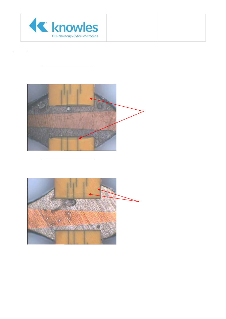
Application Note
Reference No: AN0011
Solder Alloy Choice for
Through Hole Ceramic
Discoidal & Planar Array
Capacitors Issue 8
Page 9 of 26
Results
1) Solder Type 62Sn/36Pb/2Ag
Sample 1 (Forced cooling)
80% of the joints sectioned had longbow cracks adjacent to the solder joint. All the
joints inspected had some cracking present in the ceramic, mostly corner cracks..
Sample 2 (Gradual cooling)
20% of the joints sectioned had longbow cracks adjacent to the solder joint. A total of
60% of joints had corner cracks associated with the solder meniscus.
Fig 11
Example of 62Sn/36Pb/2Ag
solder joint showing
longbow and corner cracks
Fig 10
Example of force cooled
62Sn/36Pb/2Ag solder joint
showing longbow and corner
cracks
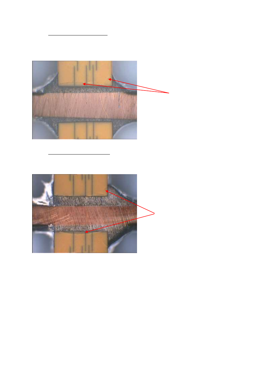
AN0011 Issue 8 – Solder Alloy Choice
CN# P109825
2) Solder Type 60Sn/40Pb
Sample 1 (Forced cooling)
All of the joints sectioned had longbow cracks adjacent to the solder joint. All joints also
has corner cracks.
Sample 2 (Gradual cooling)
60% of the joints sectioned exhibited longbow cracks adjacent to the solder joint. A
total of 80% of joints had corner cracks associated with the solder meniscus.
Fig 13
Example of 60Sn/40Pb solder
joint showing longbow and
corner cracks
Fig 12
Example of force cooled
60Sn/40Pb solder joint
showing longbow and corner
cracks
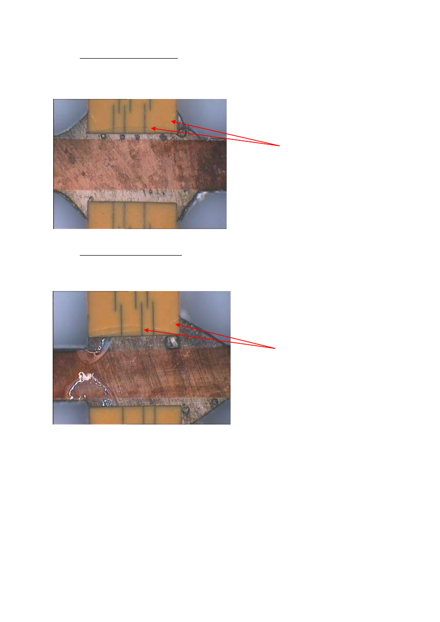
AN0011 Issue 8 – Solder Alloy Choice
CN# P109825
3) Solder Type 99.3Sn/0.7Cu
Sample 1 (Forced cooling)
All of the joints sectioned had longbow cracks adjacent to the solder joint. All joints also
has corner cracks.
Sample 2 (Gradual cooling)
All of the joints sectioned had longbow cracks adjacent to the solder joint. All joints also
has corner cracks.
Fig 15
Example of 99.3Sn/0.7Cu
solder joint showing longbow
and corner cracks
Fig 14
Example of force cooled
99.3Sn/0.7Cu solder joint
showing longbow and corner
cracks
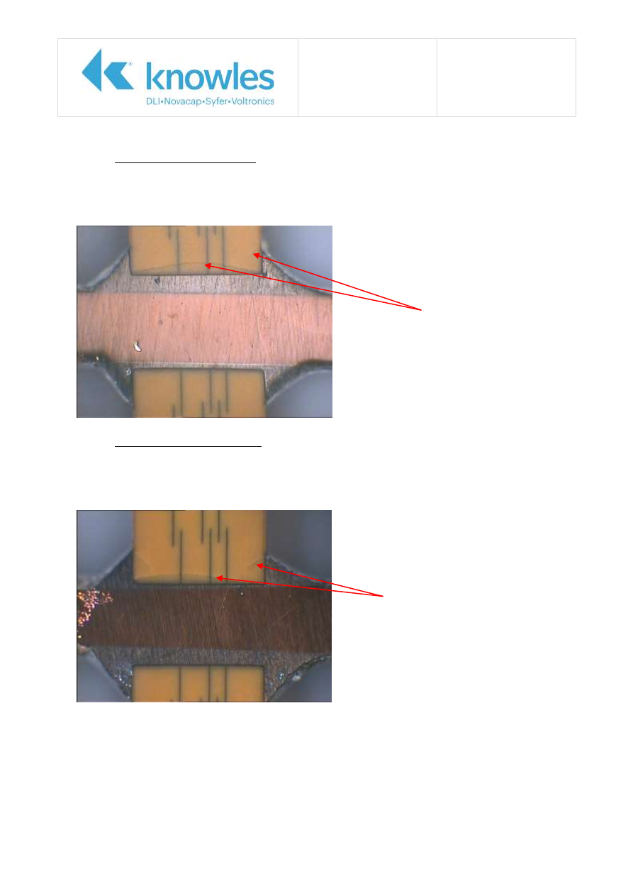
Application Note
Reference No: AN0011
Solder Alloy Choice for
Through Hole Ceramic
Discoidal & Planar Array
Capacitors Issue 8
Page 12 of 26
4) Solder Type 95.5Sn/3.8Ag/0.7Cu
Sample 1 (Forced cooling)
All of the joints sectioned had longbow cracks adjacent to the solder joint. All joints also
has corner cracks.
Sample 2 (Gradual cooling)
40% of the joints sectioned had longbow cracks adjacent to the solder joint. 80% of the
joints in total had corner cracks, mainly corner cracks associated with solder pads.
Fig 17
Example of 95.5Sn/3.8Ag/0.7Cu
solder joint showing longbow and
corner cracks
Fig 16
Example of force cooled
95.5Sn/3.8Ag/0.7Cu solder
joint showing longbow and
corner cracks
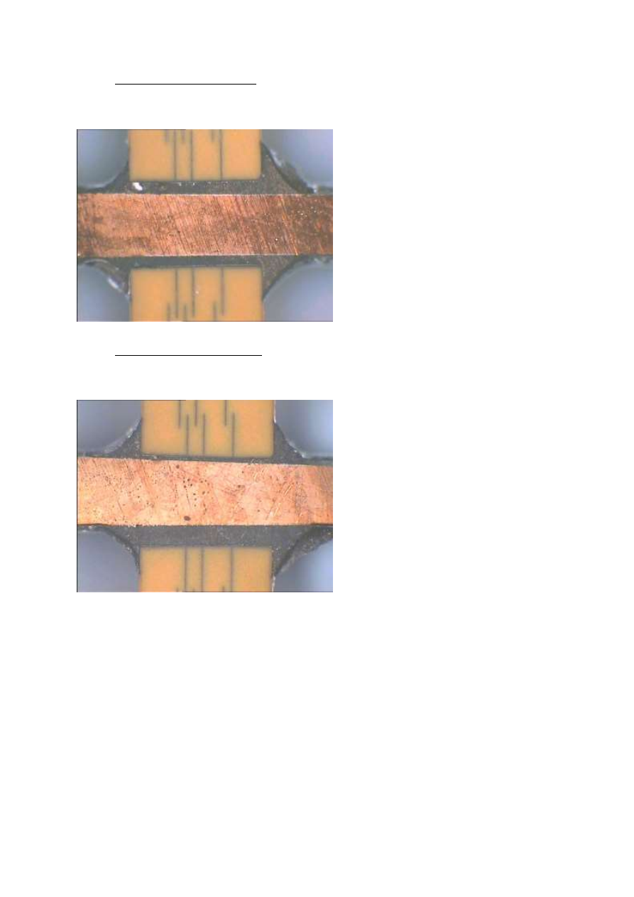
AN0011 Issue 8 – Solder Alloy Choice
CN# P109825
5) Solder Type 50In / 50Pb
Sample 1 (Forced cooling)
None of the joints sectioned exhibited any sign of induced cracks in the ceramic.
Sample 2 (Gradual cooling)
None of the joints sectioned exhibited any sign of induced cracks in the ceramic.
Fig 19
Example of 50Pb/50In solder
joint showing absence of any
cracks
Fig 18
Example of force cooled
50Pb/50In solder joint
showing absence of any
cracks
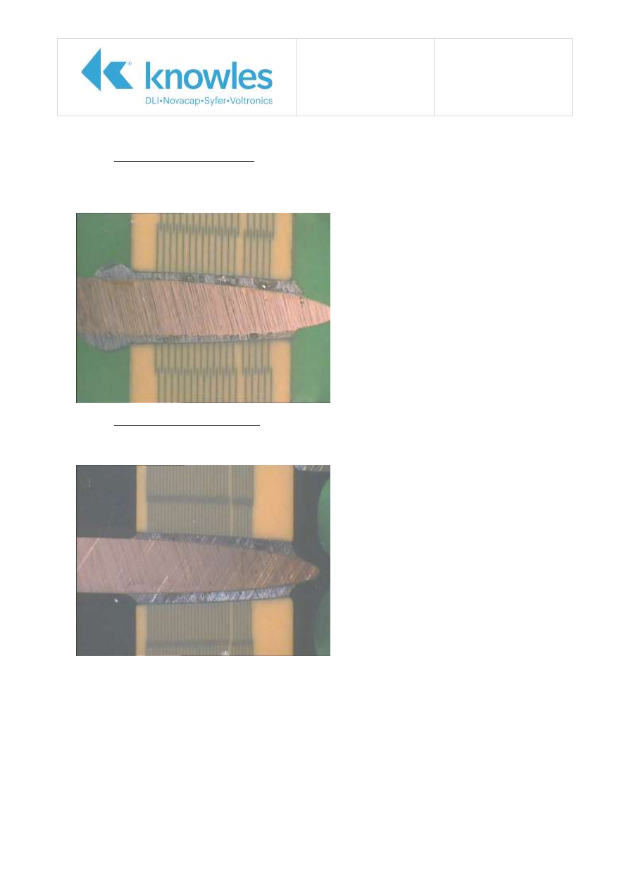
Application Note
Reference No: AN0011
Solder Alloy Choice for
Through Hole Ceramic
Discoidal & Planar Array
Capacitors Issue 8
Page 14 of 26
6) Solder Type 95Pb / 5In
Sample 1 (Forced cooling)
None of the joints sectioned exhibited any sign of induced cracks in the ceramic.
Sample 2 (Gradual cooling)
None of the joints sectioned exhibited any sign of induced cracks in the ceramic.
Fig 20
Example of force cooled
95Pb/5In solder joint showing
absence of any cracks
Fig 21
Example of 95Pb/5In solder
joint showing absence of any
cracks
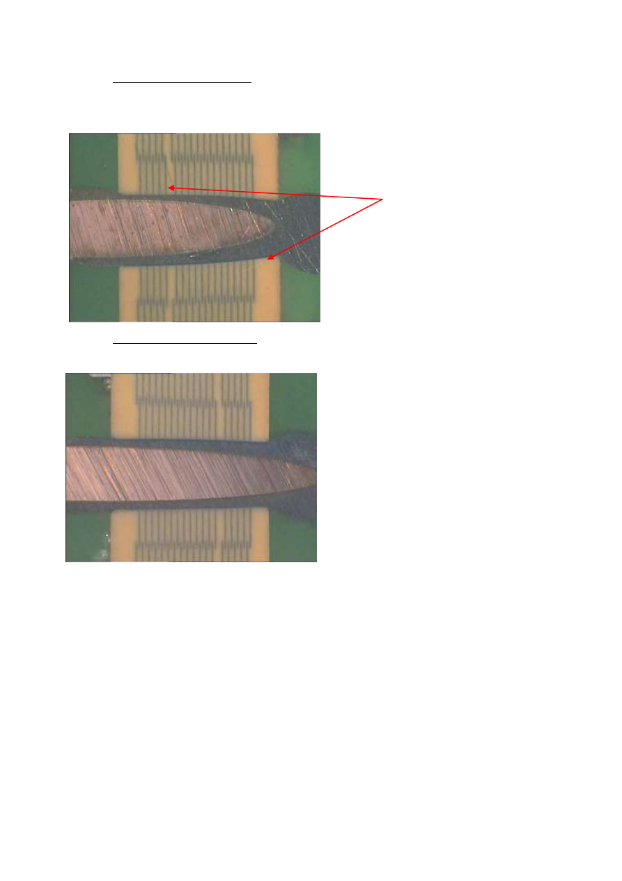
AN0011 Issue 8 – Solder Alloy Choice
CN# P109825
7) Solder Type 93.5Pb/5Sn/1.5Ag
Sample 1 (Forced cooling)
10% of the joints inspected showed very small longbow cracks adjacent to the solder
joint. These were noticeably smaller than the cracks seen in other samples.
Sample 2 (Gradual cooling)
None of the joints sectioned exhibited any sign of induced cracks in the ceramic.
Fig 22
Example of 93.5Pb/5Sn/1.5Ag
solder joint showing small longbow
cracks.
Fig 23
Example of 93.5Pb/5Sn/1.5Ag
solder joint showing absence of
any cracks
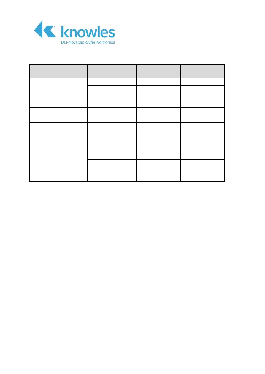
Application Note
Reference No: AN0011
Solder Alloy Choice for
Through Hole Ceramic
Discoidal & Planar Array
Capacitors Issue 8
Page 16 of 26
Results Summary
Alloy Type
Cooling
% Defective
‘Longbow’ only
% Defective
Total
62Sn/36Pb/2Ag
Forced
80
100
Gradual
20
60
60Sn/40Pb
Forced
100
100
Gradual
60
80
99.3Sn/0.7Cu
Forced
100
100
Gradual
100
100
95.5Sn/3.8Ag/0.7Cu
Forced
100
100
Gradual
40
80
50Pb/50In
Forced
0
0
Gradual
0
0
95Pb/5In
Forced
0
0
Gradual
0
0
93.5Pb/5Sn/1.5Ag
Forced
10
10
Gradual
0
0
Note:
The HMP solder joints were made using capacitors without solder pads as available jigging did
not allow padded parts to be assembled. This eliminated corner cracking and may have slightly
distorted the results with respect to this. However, the very low level of longbow cracking
found in HMP soldered parts (10% of force cooled 93.5Pb/5Sn/1.5Ag joints only) still indicates
the improved performance of these alloys.

Application Note
Reference No: AN0011
Solder Alloy Choice for
Through Hole Ceramic
Discoidal & Planar Array
Capacitors Issue 8
Page 17 of 26
Demonstration of effect with PdAg termination
PdAg terminations raise another problem with soldering to through holes in ceramic - the termination
to ceramic bond is reduced when compared to gold plating. The effect of this is that the contraction
forces tend to stress relieve the assembly at the termination / ceramic interface rather than inside the
ceramic structure in the form of a crack.
On the face of it, this may appear better than a potentially fatal crack, but it raises a potentially more
worrying concern.
If a ceramic capacitor is cracked, and subsequently fails, then the resulting fail is almost always a short
circuit IR failure. This is normally immediately apparent and the resulting failure can be isolated and
removed.
Failure of the termination / ceramic interface will tend not to cause an immediate obvious failure, but
will instead result in loss of the filtering performance, often due to dropping capacitance. There have
been cases of total loss of filtering due to total failure of the termination / ceramic interface. Loss of
filtering may not be immediately apparent, but the effect on the performance of the overall system can
be far worse.
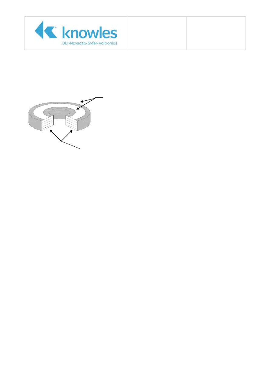
Application Note
Reference No: AN0011
Solder Alloy Choice for
Through Hole Ceramic
Discoidal & Planar Array
Capacitors Issue 8
Page 18 of 26
Testing PdAg termination and Pb free solder alloy
To demonstrate the problems experienced with soldering to PdAg termination it is easiest to consider a
design of capacitor where the capacitance is constructed without electrodes connected to the through
hole.
The capacitance is created by the interaction of the internal bore termination and the outer earth
electrodes.
The advantage of carrying out experiments with this type of construction is that any failure of the
internal termination or ceramic cracking is demonstrated by a drop in the capacitance. This is because
of the introduction of an alternative dielectric material – air – in the area of the failure.
Tests were carried out using capacitor arrays with the electrical design shown above and terminated
with PdAg termination material. Prior to assembly, the capacitance of the holes with this design was
recorded. The assembly was soldered using 95.5Sn/3.8Ag/0.7Cu solder and hot air reflow. After
assembly, the capacitance was re-measured and the results tabulated below.
Fig 24
Typical Stray Cap. Discoidal
Construction
Internal electrode Structure – Note no electrodes
connected to internal bore of capacitor
Metallised or
plated termination
area
Application Note
Reference No: AN0011
Solder Alloy Choice for
Through Hole Ceramic
Discoidal & Planar Array
Capacitors Issue 8
Page 19 of 26
Test Results
Array No. 1
Array No. 2
Start
Capacitance
(pF)
Capacitance
after Soldering
(pF)
Change (%)
Start
Capacitance
Capacitance
after Soldering
Change (%)
551
296
-46.3
539
331
-38.6
550
242
-56.0
540
256
-52.6
550
300
-45.5
535
196
-63.4
552
249
-54.9
536
189
-64.7
553
244
-55.9
532
323
-39.3
546
474
-13.2
538
151
-71.9
544
351
-35.5
536
91
-83.0
543
418
-23.0
539
175
-67.5
551
339
-38.5
544
353
-35.1
551
520
-5.6
536
168
-68.7
546
368
-32.6
536
176
-67.2
550
289
-47.5
534
317
-40.6
544
451
-17.1
544
173
-68.2
544
443
-18.6
543
153
-71.8
550
242
-56.0
543
285
-47.5
Array No. 1
Array No. 2
Mean Drop = 36.5%
Mean Drop = 58.7%
Maximum Drop = 56.0%
Maximum Drop = 83.0%
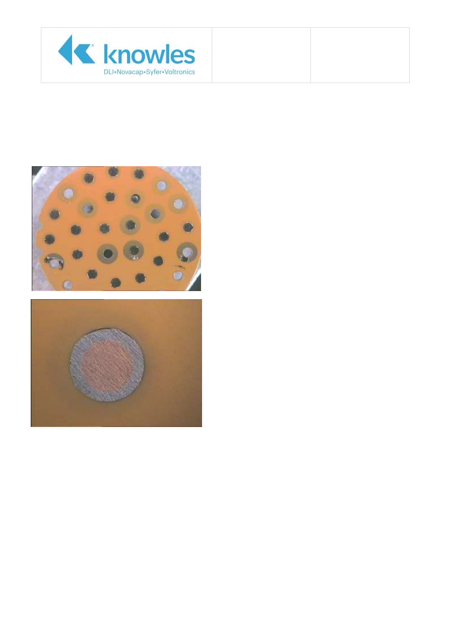
Application Note
Reference No: AN0011
Solder Alloy Choice for
Through Hole Ceramic
Discoidal & Planar Array
Capacitors Issue 8
Page 20 of 26
Analysis of the Cause of failure
The capacitor arrays were surface sectioned to check for the presence of cracks in the ceramic. Using
this method of sectioning analysis allows us to investigate all solder joints at once. If cracks are found,
they will be of the ‘Comma’ variety described above.
Surface sectioning of both arrays found no ceramic cracks.
We can therefore conclude that the capacitance loss is not caused by cracks within the ceramic in the
same way that gold terminated parts are affected.
One effect that can be seen from the surface sections above is that of solder / termination pull – away
from the bore of the ceramic. This has the same effect as the cracks in gold plated parts, introducing a
section of air dielectric within the capacitor build.
This effect can be seen in FIG 26 above. A further example is below:
Fig 25
Surface Section of Array No. 2
showing absence of damage to
ceramic
Fig 26
Close-up of Surface Section of Array
No. 1 showing absence of damage to
ceramic
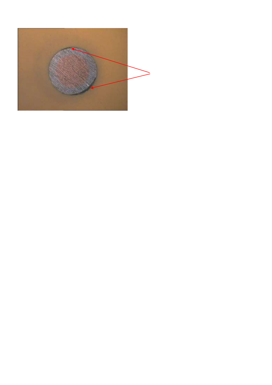
AN0011 Issue 8 – Solder Alloy Choice
CN# P109825
It is our conclusion that the unacceptable capacitance drop is caused by the failure of the termination /
ceramic bond when exposed to excessive stress force as the solder / pin joint cools.
Fig 27
Second Close-up of Surface Section of
Array No. 1 showing absence of damage
to ceramic, but evidence of pull away of
solder / termination from ceramic
surface
.
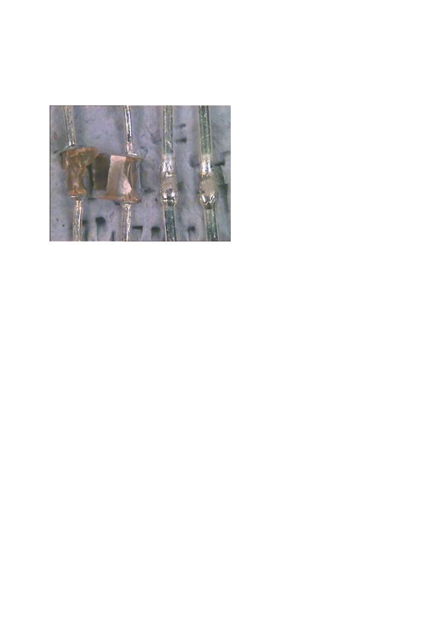
AN0011 Issue 8 – Solder Alloy Choice
CN# P109825
Analysis of the differences between gold plate and PdAg terminations
To understand the failure mode above, it is necessary to investigate the differences between PdAg
termination and gold plate.
1.
With PdAg termination, the bond to the ceramic is far weaker than gold plate termination. This
can be demonstrated by a simple pull test, as below.
As can be seen above, the gold plated termination has a far greater adhesion to the ceramic,
demonstrated by the amount of ceramic material still attached to the pin. By comparison, the
PdAg termination has been cleanly removed from the ceramic with no ceramic material
removed. Pins 3 and 4 do show the PdAg termination still attached to the solder – identified by
the dull grey areas on the solder.
This is further shown in FIG 29, where the pins have been removed from a partially sectioned
array soldered with PdAg termination.
Fig 28
Silver plated copper pins
soldered into planar array
capacitors using
95.5Sn/3.8Ag/0.7Cu solder and
removed by simply pulling out
using a pair of pliers.
Pins 1 & 2 have been pulled
from an array terminated with
gold plate.
Pins 3 & 4 have been pulled
from an array terminated with
PdAg fritted termination.
1
4
3
2
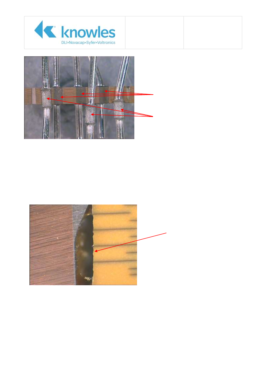
Application Note
Reference No: AN0011
Solder Alloy Choice for
Through Hole Ceramic
Discoidal & Planar Array
Capacitors Issue 8
Page 23 of 26
The ceramic exhibits no damage, and the pins are very easily removed – the termination has
relatively little adhesion to the ceramic.
2.
Secondly, PdAg termination is far more susceptible to leaching into the molten solder as the
joint is formed. In sectioned components, this is observed as areas of missing termination
within the bore of the component.
Leaching is far more common with Pb free alloys, and has been observed on PdAg terminated
components with all Pb free alloys. The following examples have been soldered using
95.5Sn/3.8Ag/0.7Cu solder alloy.
Fig 29
Example of PdAg terminated
planar array capacitor soldered
with 95.5Sn/3.8Ag/0.7Cu
solder.
As the component is sectioned,
the pins can be easily removed
without damage to the ceramic.
Note the dark grey on the solder
joint – this is the termination,
which has been removed along
with the pin & solder.
Fig 30
Termination leached away
from this area.
These electrodes have lost
contact and will result in a
potential reduction in
filtering performance.
AN0011 Issue 8 – Solder Alloy Choice
CN# P109825
This leaching also has the effect of reducing the termination adhesion between the termination
and the ceramic.
Comments on fritted termination in discoidal and planar capacitors
From this analysis it is clear that PdAg terminations are not suitable for through hole ceramic devices
when soldered with lead free solder alloys. Although the ceramic does not crack in the same way as
gold plated terminated parts do, the joint between the termination and the ceramic is compromised
resulting in a parametric failure.
It is important to also understand that the results given in this paper only represent analysis after the
soldering operation. It is normal practise for this type of component to be subjected to positive and
negative thermal excursions during testing and operation. It is reasonable to expect that the effect
can propagate during these excursions, with the possible conclusion of total joint failure.
The possible loss of up to 83% of design capacitance is clearly unacceptable, but may not be
immediately apparent in operation. Components which have had cracks induced (i.e. gold plated
termination) are likely to fail short circuit – a failure mode that is immediately observed allowing the
failed component to be isolated and removed.
Parametric failure, such as loss of capacitance, is a far more insidious failure mode in that it may not
be easily detected, but can cause serious and significant problems in operation.
In the example above, the design capacitance is 500pF, giving a typical PI filter (1000pF total)
insertion loss of 6dB @ 10MHz. If we assume that this capacitance can drop to typically 250pF (500pF
total - 50% drop), then the resultant insertion loss will only be in the region of 2dB @ 10Mhz. The
generally accepted cut-off point for a filter to be operating is 3dB. In it’s failed form the filter is not
acting as such.
This failure may not be immediately critical, but the filter is not working to it’s design performance. If
at some point in time, the filtering performance at this frequency is critical, then the performance is
not available.
Fig 31
Further example of leaching
and poor solder joint with
PdAg termination.

Application Note
Reference No: AN0011
Solder Alloy Choice for
Through Hole Ceramic
Discoidal & Planar Array
Capacitors Issue 8
Page 25 of 26
Conclusions
1.
Potentially fatal cracks were found in all assemblies manufactured with both conventional tin
lead solders and the proposed lead free alloys and gold plated termination.
2.
Tin lead alloys induced cracks in the ceramic dielectric and should not be used for the
manufacture of these assemblies.
3.
Lead free alloys performed worse of all solders under test, and should not be used for the
manufacture of these assemblies. The lead free alloys tended to perform worse than the tin
lead alloys – more cracks and larger cracks were found.
4.
In order to manufacture reliable safe capacitor assemblies, it is essential to use a ductile solder
so as to prevent excessive force being transferred to the ceramic dielectric material. Ductile
solders tend to be an alloy of lead and indium.
5.
High melting point alloys, typically containing >90% lead and melting around 300ºC, are
acceptable if indium is to be avoided - but have a narrower processing window and are more
susceptible to problems if the cooling rate is not controlled.
6.
Solder joint design should be given due consideration. In particular, solder pads should be
reduced or minimised (Note – the manufacture and testing of the capacitor itself will sometimes
demand solder pads are included)
7.
Gradual cooling should be used and force cooling, either intentional or unintentional due to
factors such as drafts, should be avoided.
8.
PdAg terminations reduce the incidence of ceramic cracking, but may result instead in
parametric failure of the capacitor. This can be ultimately worse in service.
9.
It is clear that there is a conundrum – if the termination system provides a very good bond to
the ceramic, then there is a risk of cracking the ceramic. If the termination system provides a
weak bond to the ceramic then there is a risk of parametric failure leading to loss of
performance.
10.
The best option for reliable performance is to use a termination system that provides a very
strong bond to the ceramic (e.g. gold) and introduce stress relief through the use of ductile
solders.

Application Note
Reference No: AN0011
Solder Alloy Choice for
Through Hole Ceramic
Discoidal & Planar Array
Capacitors Issue 8
Page 26 of 26
RoHS compliance
EU directive 2011/56/EU (superseding 2002/95/EC), commonly known as RoHS directive, limits the
use of certain substances in electronics manufacture. These substances include lead, which has forced
a change from lead containing solders to lead free solders for a majority of applications.
Clearly from the evidence shown above, the use of lead free solders should be avoided when soldering
to ceramic discoidal and planar capacitors.
The directive allows for exemptions to be granted for situations where there is no technical alternative
or such alternatives constitute a negative environmental impact. Syfer have successfully applied for
the use of lead containing solders for soldering to ceramic planar arrays and discoidal capacitors to be
made exempt from the directive.
This exemption is detailed in the annex to the directive as follows:
Exemption No. 24
Lead in solders for the soldering to machined through hole discoidal and planar
array ceramic multilayer capacitors.
Issued in the addendum to directive 2002/95/EC dated 14
th
October 2006 and continued in the revised
directive 2011/56/EU of 1
st
July 2011.
To summarise – Filters, filter assemblies and filtered connectors manufactured with Syfer discoidal and
planar capacitors can be assembled using lead bearing solder alloys – i.e. InPb – to eliminate the
incidence of micro cracking due to mismatched material shrinkages and still be RoHS compliant in this
respect.

AN0012 Issue 4 – Electronic Lighting Ballasts
CN# P109825
Electronic Lighting Ballasts
Effective Series Resistance (ESR) ...............................................................3
Knowles (UK) Limited,
Old Stoke Road, Arminghall, Norwich,
Norfolk, NR14 8SQ, United Kingdom
Tel: +44 (0) 1603 723300
Tel. (Sales): 01603 723310
Fax: +44 (0) 1603 723301
www.knowlescapacitors.com/syfer
Application Note
Reference No: AN0012
Electronic Lighting
Ballasts Issue 4
Page 2 of 5
Introduction
All fluorescent lamps require a ballast to provide the electrical power to preheat the lamp electrodes,
strike the lamp, provide the running power and control the discharge current. This can be achieved by
either electromagnetic or high frequency electronic ballasts. With the introduction of new regulations in
2005 covering the European Union, USA and Japan, the use of the older electromagnetic ballasts will
no longer be permitted, apart from repairing older systems until 2010. High frequency electronic
ballasts provide increased luminous flux from the fluorescent lamp and negate the need for a starter,
thus saving energy and costs.
With more manufacturers of high frequency electronic ballasts converting to low cost surface mount
capacitors, for use in the snubber circuit of the ballast, Syfer Technology Ltd has introduced a range of
capacitors specifically intended for this application. This range is available in the popular 1206 case size
and is manufactured from the stable COG/NPO dielectric. This is particularly suitable for the ballast
operating frequencies of 20KHz to 100KHz.
The range features capacitance values up to 1nF, with a maximum peak to peak voltage of 600V over
a wide operating frequency range (see below).
<= 270pF
= 330pF
= 390pF
= 470pF
= 560pF
= 680pF
= 820pF
=1nF
Maximum Pk to Pk Voltage @ 100°C
0
100
200
300
400
500
600
700
100
1000
10000
100000
1000000
Frequency Hz
P
k
t
o
P
k
V
o
lt
a
g
e
Application Note
Reference No: AN0012
Electronic Lighting
Ballasts Issue 4
Page 3 of 5
Effective Series Resistance (ESR)
The low, stable ESR (see below) of this range, particularly at the ballast operating frequency 20 to
100KHz, results in a wide operating ambient temperature range of –55°C to +100°C.
100pF
270pF
470pF
680pF
1nF
Typical ESR Values
0.1
1
10
100
1000
10000
100000
100
1000
10000
100000
1000000
Frequency Hz
E
S
R
O
h
m
s
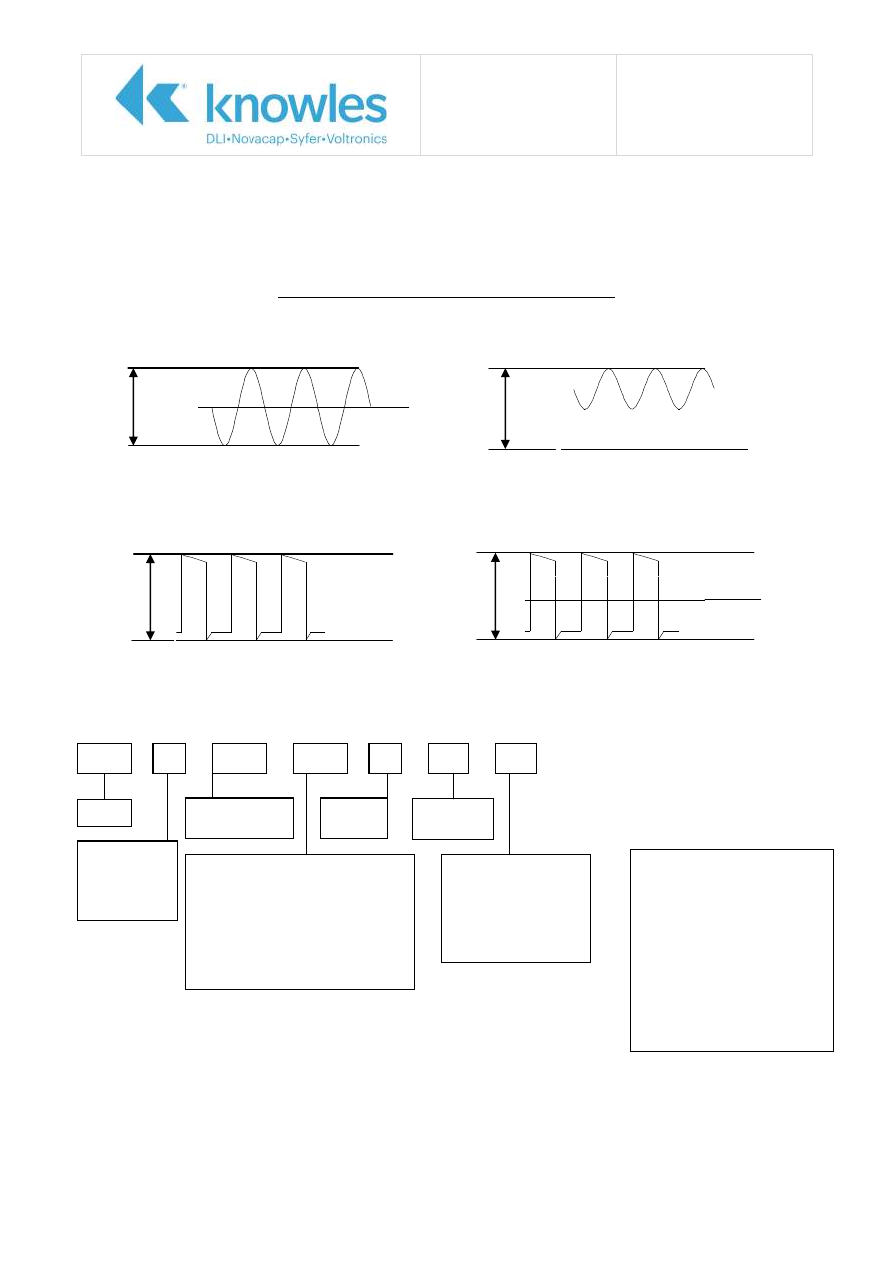
Application Note
Reference No: AN0012
Electronic Lighting
Ballasts Issue 4
Page 4 of 5
Pk to Pk Voltage
Voltage waveforms produced in ballasts result in very high dv/dt figures, this range is capable of
withstanding a dv/dt in excess of 5000V/uSec. The voltage waveforms used may be of several varying
types, depending on application. The maximum peak to peak voltage should be defined as below.
Definition of maximum Pk to Pk Voltage
AC Voltage
DC + AC Voltage
Vp-p
Vp-p
0V
0V
Pulsed Voltage
Pulsed Voltage
Vp-p
Vp-p
0V
0V
The rated peak to peak voltage of 600 volts should not be exceeded in each of the above options.
Ordering Information
1808
Size
Termination
J = Nickel Barrier
Y = Flexicap
Voltage
630 = 630Vdc
1206
J
630
0681
Capacitance
First Digit = 0
Second and Third digits = Significant
figures of capacitance code
Fourth digit = Number of zeros
following e.g. 0102 = 1000pF
For values below 10pF a P is inserted
for decimal point e.g. 4P70 = 4.7pF
J
See
Table 2
C
Dielectric
C = COG
T
Packaging Options
T = Taped and Reeled
7” diameter reels
R = Taped and Reeled
13” diameter reels
B = Bulk packaging
In tubs
Table 2
Capacitance Tolerance
Nominal Cap value 4.7pF – 8.2pF
C = ± 0.25pF
D = ± 0.50pF
F = ± 1.0pF
Nominal Cap value 10pF –
1000pF
F = ± 1%
G = ± 2%
J = ± 5%
K = ± 10%
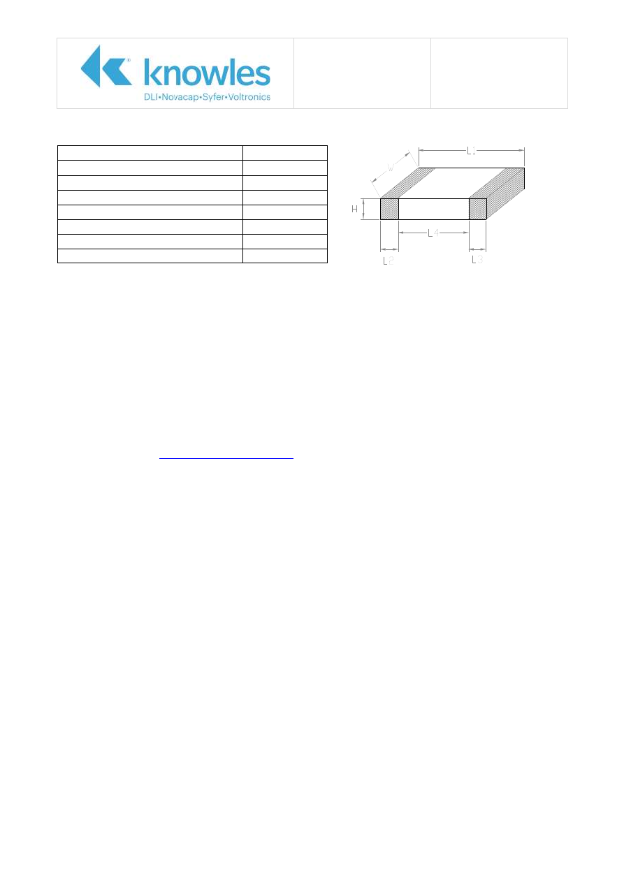
Application Note
Reference No: AN0012
Electronic Lighting
Ballasts Issue 4
Page 5 of 5
Mechanical Specification
Electrical Specification
Dielectric
: COG 0 ± 30 ppm/°C
Operating Temperature range
: -55°C to + 100°C
Dissipation Factor
: Cr > 50pF <= 0.0015
: Cr <= 50pF = 0.0015 (15+0.7)Cr
Rated Voltage
: 630Vdc/600V Peak to peak
Insulation Resistance
: >100Gohms
Voltage Proof
: 1.5 x Rated Voltage for 5 seconds
dv/dt Rating
: >5000V/uSec
Climatic Category
: 55/125/56
Ageing Rate
: Zero
For further information or technical assistance please contact our Sales Department on +44 1603
723310 or by Email at
Syfer Size
1206
Length (L1) mm
3.20 ± 0.30
Width (W) mm
1.60 ± 0.20
Thickness (H) mm
1.60 Max.
Termination Bands mm (L2, L3)
0.25 – 0.75
Creepage Distance (L4)
1.40 Min.
Termination Material
Nickel Barrier
Solderability
IEC 68-2-20

AN0013 Issue 8 – Packaging Labels
CN# P109825
Packaging Labels
Confirms that the product is RoHS compliant. .....................................3
Pb-free process information. .............................................................3
Knowles (UK) Limited,
Old Stoke Road, Arminghall, Norwich,
Norfolk, NR14 8SQ, United Kingdom
Tel: +44 (0) 1603 723300
Tel. (Sales): 01603 723310
Fax: +44 (0) 1603 723301
www.knowlescapacitors.com/syfer
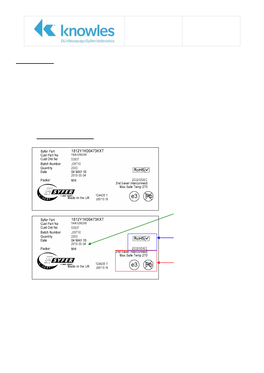
Application Note
Reference No: AN0013
Packaging Labels Issue 8
Page 2 of 3
Introduction
With the implementation of the European RoHS directive in July 2006 and the China
RoHS phase I requirements in March 2007, Syfer has received numerous RoHS
compliance questionnaires with requests for the product status to be displayed on
packaging labeling.
With respect to displaying the product status on packaging labeling, customers are
generally concerned regarding two issues:
1.
Is the product RoHS compliant?
2.
Does the product conform with Pb-free assembly process requirements?
The purpose of this application note is to explain the standard Syfer label format to
declare RoHS compliance and Pb-free process information.
Standard Label Format
Example of a standard Syfer
label with RoHS and lead-free
information
Additional date code for China
RoHS, referred to in
GB/T7408-94 standard.
The RoHS symbol states that
the product is RoHS compliant
(refer to note 1)
This section provides Pb-free
process information
based on JEDEC J-STD-609A
(refer to note 2)
Application Note
Reference No: AN0013
Packaging Labels Issue 8
Page 3 of 3
Notes
1. RoHS compliant symbol
Confirms that the product is RoHS compliant.
2. Pb-free process information.
This section on the label is based on the requirements defined by
IPC/ JEDEC J-STD-609A
Marking and Labeling of Components, PCBs and PCBAs to Identify Lead (Pb), Pb-Free and
Other Attributes.
The information defines:
The Pb-free termination finish category. Syfer components will typically be
labeled with the following (depending on customer order requirements):
e3 - Sn.
e4 - Precious Metal
That the 2
nd
level interconnect (refer to
IPC/ JEDEC J-STD-609A
) terminal
finish of components are Pb-free.
The maximum temperature that the components should attain during
assembly.
IPC/ JEDEC J-STD-609A
is available at
www.jedec.org/standards-documents
Customer Specific Labels
Where customers define specific labeling requirements, the RoHS compliant symbol
and Pb-free process information will be added onto the label (space permitting) or onto
a separate label attached to the packaging.
For further information regarding customer specific labeling requirements then please
contact Syfer Sales department at

AN0014 Issue 4 – X2Y Balanced Line EMI Chip
CN# P109825
X2Y Balanced Line EMI Chip
Reliability and Performance Data
Component Diagrams ...............................................................................2
Performance Information ..........................................................................5
Capacitance vs. Time ............................................................................5
IR vs. Temperature ...............................................................................6
DF vs. Temperature ..............................................................................7
Rated Voltage vs. Temperature...............................................................8
Temperature Coefficient ........................................................................9
Knowles (UK) Limited,
Old Stoke Road, Arminghall, Norwich,
Norfolk, NR14 8SQ, United Kingdom
Tel: +44 (0) 1603 723300
Tel. (Sales): 01603 723310
Fax: +44 (0) 1603 723301
www.knowlescapacitors.com/syfer
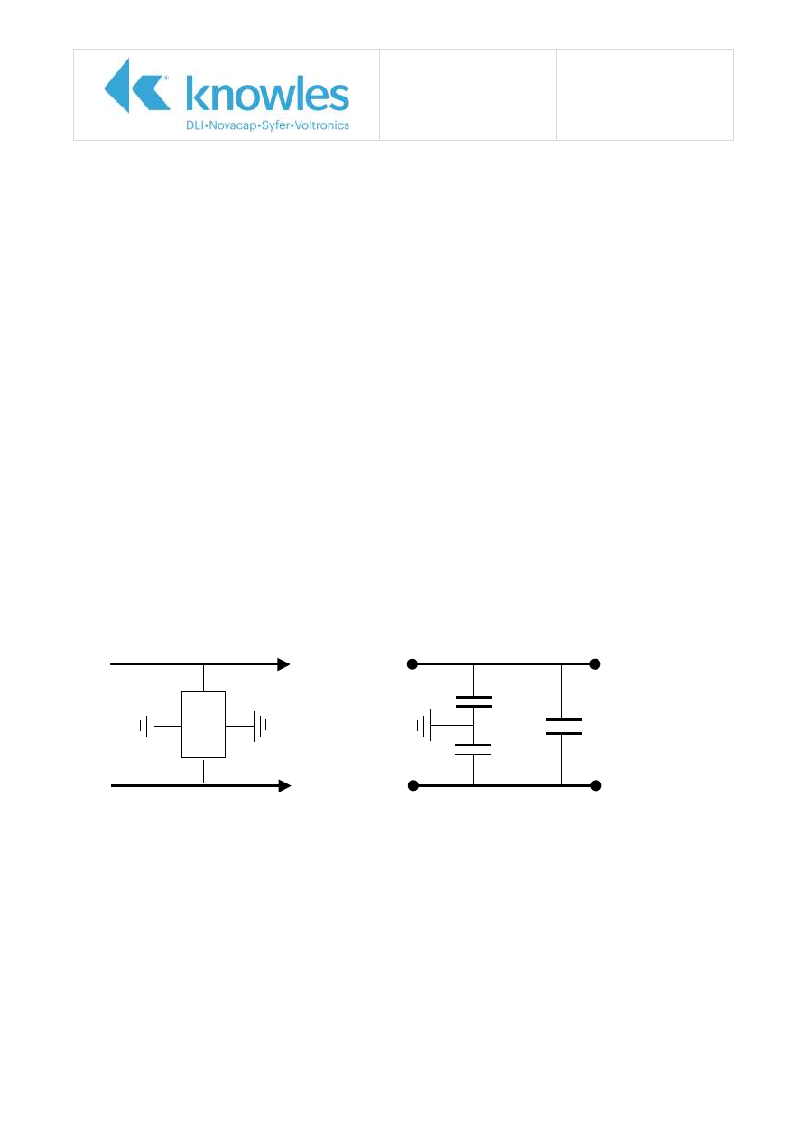
Application Note
Reference No: AN0014
X2Y Balanced Line EMI
Chip Issue 4
Page 2 of 10
Introduction
The X2Y Balanced Line EMI Chip is a 3 terminal device with a revolutionary internal
design, offering simultaneous line-to-line and line-to-ground filtering, using a single
chip. The novel electrode structure provides a much reduced inductance when
compared to conventional capacitors, which enhances the high frequency filtering
performance.
Capable of replacing two or more conventional devices, typical applications include
the suppression of EMI in DC motors for automotive products, eg window lifters,
mirror motors, seat adjustment etc.
X2Y components are available in case sizes of 0805 up to 2220, capacitance values
from 10pF to 1.2uF.
Specifications
Dielectric:
X7R or C0G/ NP0
Capacitance Measurement:
At 1000hr point
Typical Capacitance Matching: Better than 5%
Temperature Rating:
-55°C to 125°C
Dielectric Withstand Voltage: 2.5 x Rated Volts for 5 secs.
Charging current limited to 50mA max.
Insulation Resistance:
100GOhms or 1000S (whichever is the less).
Termination Material:
Nickel Barrier.
Component Diagrams
Line A
A
A
C1
C2
Ground
C1
Line B
B
B

Application Note
Reference No: AN0014
X2Y Balanced Line EMI
Chip Issue 4
Page 3 of 10
Technical Benefits
Simultaneous line-to-line and line-to-ground filtering in one device.
Replaces chokes, inductors, and capacitors with an SMT single chip solution.
Reduces 2 or more components with one device.
Matched capacitance line-to-ground on both lines.
Low inductance due to cancellation effect.
Differential and common mode attenuation.
Effects of temperature and voltage variation eliminated.
Applications
Balanced lines.
Twisted pairs.
EMI suppression on DC motors.
Sensor/ transducer applications.
Wireless communications.
Audio.
Reliability Information
Load Test
Samples taken during the development process and from production batches
have been subjected to a standard load test. Load test information and results:
Time period analyzed:
1997 to 06 January 2005.
Number of capacitors tested: 10270
Product group analysed:
All X2Y products sample tested.
Testing location:
Syfer Reliability Test Department.
Endurance test conditions:
Up to 1000 hours with 1.5x Rated Voltage applied
at 125
C.
Results:
6 failures in 10,215,360 component test hours.
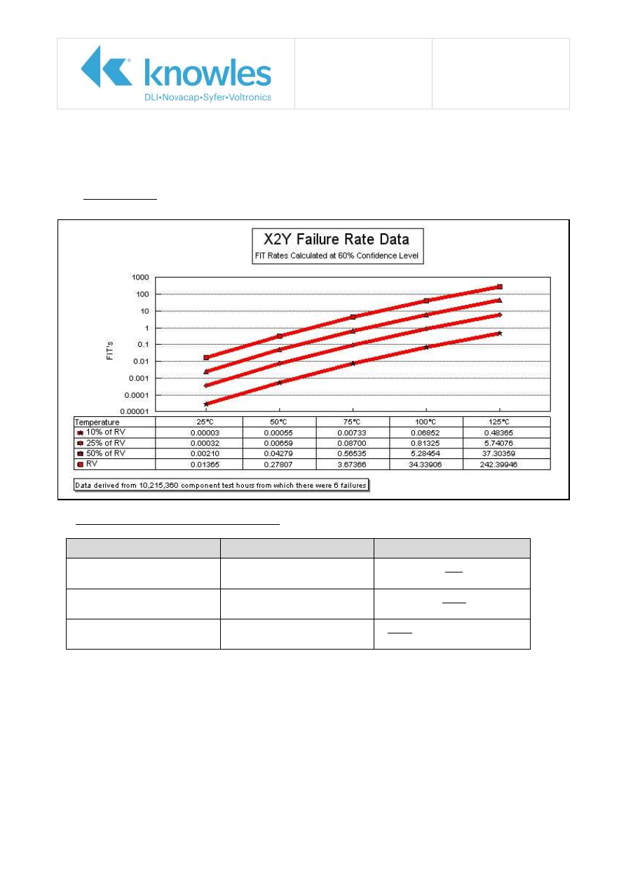
Application Note
Reference No: AN0014
X2Y Balanced Line EMI
Chip Issue 4
Page 4 of 10
The load test results have then been used to calculate FIT (Failure In Time) rates by
applying voltage and temperature acceleration factors.
For details regarding the FIT rate calculation method including acceleration factors
then refer to Syfer application note reference AN0004.
X2Y FIT Rates
FIT Rate Reliability Conversion Factors
From
To
Operation
FITS
MTBF (Years)
10
9
(FITS
8760)
FITS
Failure Rate Per Hour
FITS
10
9
FITS
ppm (1 year)
FITS x 8760 x 1,000,000
10
9
FITS = Failures in 10
9
Hours
MTBF = Mean Time Between Failure
Application Note
Reference No: AN0014
X2Y Balanced Line EMI
Chip Issue 4
Page 5 of 10
Humidity Tests
Samples taken during the development process and from production batches
have been subjected to a standard humidity test. Humidity test information and
results:
Time period analyzed:
1997 to 06 January 2005.
Number of capacitors tested: 719
Product group analysed:
All X2Y products sample tested.
Testing location:
Syfer Reliability Test Department.
Endurance test conditions:
Up to 1000 hours with 85
C/85%RH with 1.5Vdc
or 5Vdc applied.
Results:
0 failures in 552,600 component test hours.
Performance Information
Capacitance vs. Time
Typical COG performance:
Typical COG Capacitance vs Time
-3
-2
-1
0
1
2
3
0.1
1
10
100
1000
10000
100000
Hours
D
e
lt
a
C
,%
Application Note
Reference No: AN0014
X2Y Balanced Line EMI
Chip Issue 4
Page 6 of 10
Typical X7R performance:
Typical X7R Capacitance vs Time
-3
-2
-1
0
1
2
3
4
5
0.1
1
10
100
1000
10000
100000
Hours
D
e
lt
a
C
,%
IR vs. Temperature
Typical COG performance:
Greater than 100GOhms or 1000S over the operating temperature range.
Typical X7R performance:
Typical
I.R vs Temperature
-15
-10
-5
0
5
10
15
20
25
20
40
60
80
100
120
140
Temp °C
%
C
h
a
n
g
e
f
ro
m
r
o
o
m
T
e
m
p
Application Note
Reference No: AN0014
X2Y Balanced Line EMI
Chip Issue 4
Page 7 of 10
DF vs. Temperature
Typical maximum COG performance:
Dissipation Factor vs Temperature
COG
0
0.2
0.4
0.6
0.8
1
-55
-35
-15
5
25
45
65
85
105
125
Temperature °C
D
is
s
ip
a
ti
o
n
F
a
c
to
r
%
Typical X7R performance:
Dissipation Factor vs Temperature
X7R
0
0.5
1
1.5
2
2.5
3
3.5
-55
-35
-15
5
25
45
65
85
105
125
Temperature °C
D
is
s
ip
a
ti
o
n
F
a
c
to
r
%
Application Note
Reference No: AN0014
X2Y Balanced Line EMI
Chip Issue 4
Page 8 of 10
Rated Voltage vs. Temperature
Typical COG performance:
Rated Voltage vs Temperature
COG
0
20
40
60
80
100
120
-55
-35
-15
5
25
45
65
85
105
125
Temperature °C
%
o
f
R
a
te
d
V
o
lt
a
g
e
Typical X7R performance:
Rated Voltage vs Temperature
X7R
0
20
40
60
80
100
120
-55
-35
-15
5
25
45
65
85
105
125
Temperature °C
%
o
f
R
a
te
d
V
o
lt
a
g
e
Application Note
Reference No: AN0014
X2Y Balanced Line EMI
Chip Issue 4
Page 9 of 10
Temperature Coefficient
Typical COG performance:
Temperature Coefficient
COG
-40
-30
-20
-10
0
10
20
30
40
-55
-35
-15
5
25
45
65
85
105
125
Temperature °C
D
e
lt
a
C
p
p
m
/°
C
Upper lim it
Low er lim it
Typical X7R performance:
Typical Temperature Coefficient
X7R
-16
-14
-12
-10
-8
-6
-4
-2
0
2
4
-55
-45
-35
-25
-15
-5
5
15
25
35
45
55
65
75
85
95
105
115 125
Temperature °C
%
C
ha
ng
e
f
rom
R
oo
m
Te
m
p
Application Note
Reference No: AN0014
X2Y Balanced Line EMI
Chip Issue 4
Page 10 of 10
Voltage Coefficient
Typical COG performance:
Voltage Coefficient
COG
0
20
40
60
80
100
120
10
20
30
40
50
60
70
80
90
100
% of Rated Voltage
C
a
p
a
c
ita
n
c
e
%
Typical X7R performance (50DCV Rated):
Typical Voltage Coefficient
X7R
0
10
20
30
40
50
60
70
80
90
100
0
10
20
30
40
50
Applied DC Voltage
C
a
pac
it
a
nce
%

AN0016 Issue 5 – Micro sectioning of MLCC
CN# P109825
Micro sectioning Of Multilayer
Ceramic Capacitors
Introduction ............................................................................................2
Examples of Sectioning Artifacts ................................................................4
Knowles (UK) Limited,
Old Stoke Road, Arminghall, Norwich,
Norfolk, NR14 8SQ, United Kingdom
Tel: +44 (0) 1603 723300
Tel. (Sales): 01603 723310
Fax: +44 (0) 1603 723301
www.knowlescapacitors.com/syfer
Application Note
Reference No: AN0016
Micro-sectioning of
MLCCs Issue 5
Page 2 of 7
Introduction
Preparation of Multilayer Ceramic Capacitors micro sections involves the use of techniques
which can create artifacts, which in turn can be misinterpreted as capacitor faults. The purpose
of this document is to provide a guide to preparation and examination of micro sections, so that
results reflect the true internal properties of the parts being examined.
It is recommended that fracture sections examined using a Scanning Electron Microscope are
used in conjunction with micro sectioning, in order to gain the most information. This technique
is also detailed within this document.
Potting of Components
Components are normally applied to a double sided sticky tape, in the orientation appropriate
for examination. Components should be separated from one another by a reasonable gap to
allow potting compound to surround each component. If components are too close, they can be
poorly supported by resin, and can be damaged around the chip edges during grinding.
A suitable sized mould should be used to contain the components, so that each component is a
reasonable distance from the edge of section stub.
Choice of potting compound is very important. Use of a low price general purpose resin will
almost certainly generate damage around the chip edges during grinding. Consequently use of a
high quality, low stress potting compound is recommended.
Grinding of Micro Section
Waterproof Silicon Carbide grinding paper is available in many grit sizes. Paper should be
selected as appropriate to the sample being prepared, and the degree of finish required for
examination of the finished section. In cases where the best quality micro section is required, it
is recommended that nothing coarser than 800 grit paper is used, with 1200 grit or finer being
used prior to final polishing.
Direction of grinding is important, and can influence the results generated. Syfer has
determined that in most cases, multi directional grinding gives the best results.
It is possible to determine in some cases whether faults are real or artifacts by changing the
grinding direction periodically, and examining the micro section at each stage.
Polishing of Micro Section
It is common to use fine diamond slurries to polish micro sections. These may be of very fine
particle size (example 0.1 micron), but they have been found to create damage to Multilayer
Ceramic Capacitors, as the diamond is harder than the ceramic material being polished.
Syfer recommend the use of an alumina based polish, which does not create any damage to the
parts being polished. Syfer use a fine alumina powder, which is made into a slurry using
deionised water.
As with grinding, polishing should be multi directional.
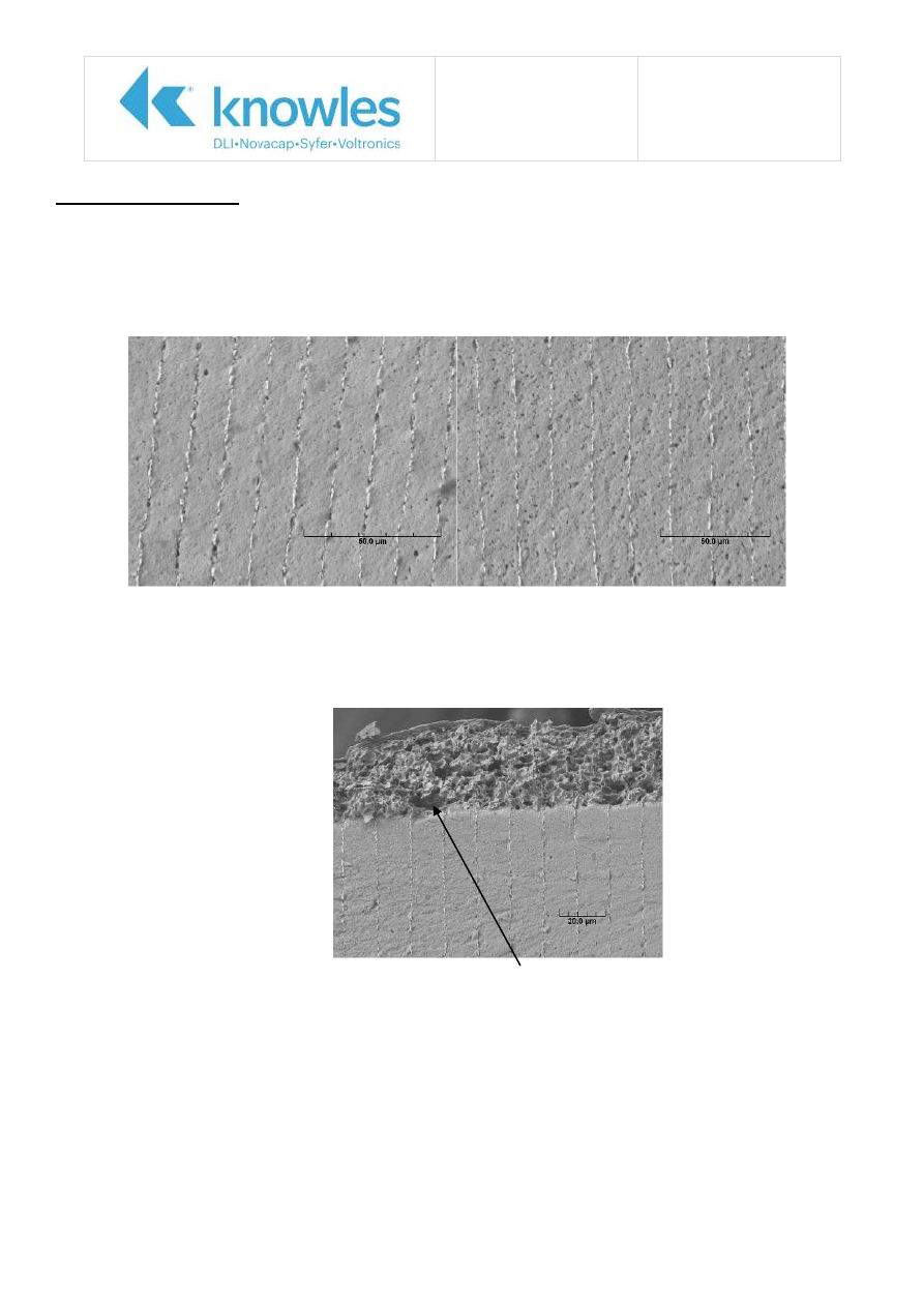
Application Note
Reference No: AN0016
Micro-sectioning of
MLCCs Issue 5
Page 3 of 7
Fracture Sections
Fracture sections are obtained by breaking a chip so that the internal electrodes are exposed.
Ease of fracturing is highly dependent on the physical dimensions of the part to be fractured. In
order to make a good fracture section, it is important to break the chip without applying too
much pressure. It may help to scribe the chip at the point where the fracture is required prior to
applying pressure. Fractured edges should be examined optically prior to using the SEM, and
only the best fractures used for detailed analysis.
Fracture Section
Fracture Section
X7R 1 – High density material
X7R 2 – Lower density material
Unfortunately, fracture sections are generally unsuitable for looking at chip / termination /
plating boundaries, as there are definite stresses applied to the termination interfaces during
fracturing, and the edges of the termination bands are particularly vulnerable.
Fracture section showing some
damage at termination boundary
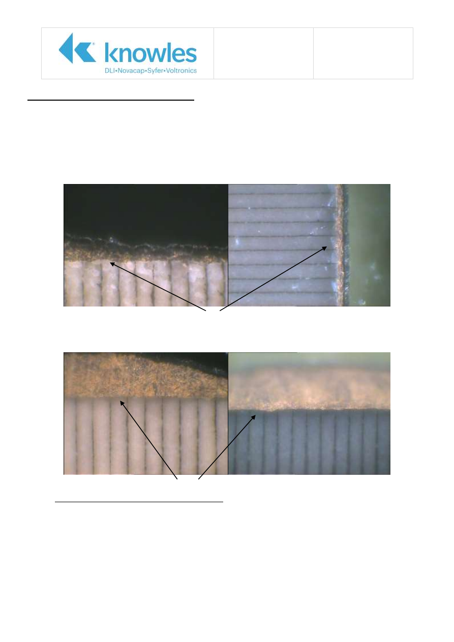
Application Note
Reference No: AN0016
Micro-sectioning of
MLCCs Issue 5
Page 4 of 7
Examples of Sectioning Artifacts
A. Termination / Chip Interface Cracking
This is an example of an artifact that may be present particularly when grinding along the
electrodes, and less evident when grinding perpendicular to the electrodes.
Stress relief between the ceramic chip and the termination can take place during grinding. This
is most common where the relative hardness of the ceramic and termination materials are
different, such as in the Syfer ‘Flexicap’ range of parts, which uses a polymeric termination
primarily to reduce mechanical cracking issues.
Cracks at termination / chip interface caused by stress relief due to unsuitable grinding
Using a refined sectioning technique, and grinding perpendicular to the electrodes, it was
possible to eliminate the cracks, confirming them as artifacts.
No cracks evident at termination / chip interface on correctly ground specimen
B. Voids Within the Dielectric Structure
Ceramic materials as used to manufacture Multilayer Ceramic Capacitors vary greatly
in fired structure. Some materials produce a denser structure than others after fire,
and grain size can vary significantly.
This means that ceramic materials can behave differently when micro sectioned and
some materials can be more prone to pull out of the fired structure than others.
Pull out occurs when the ceramic structure is damaged by the grinding process,
causing a fragment of the ceramic to be removed, leaving a void. When examined
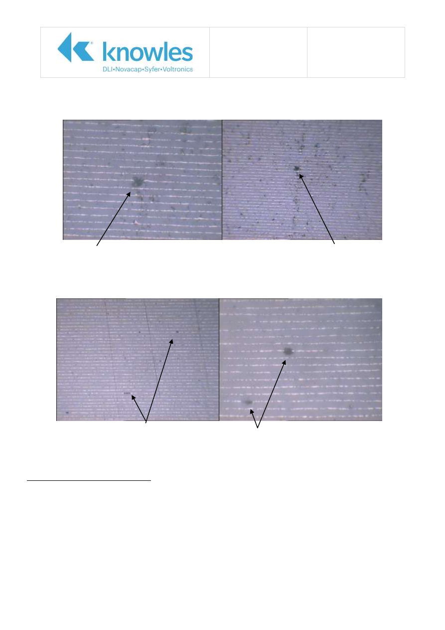
Application Note
Reference No: AN0016
Micro-sectioning of
MLCCs Issue 5
Page 5 of 7
prior to polishing it is common to see lines of pull out following the scratch marks on a
section.
Void within dielectric structure The same void, seen as pullout
Formed as part of a scratch
Depending on grinding media and technique used, it is possible to damage the
ceramic to a significant depth below the surface, meaning that the damage can still
be apparent after careful fine grinding and polishing.
Polished sections, showing voids due to pullout
In general, a genuine void will almost always be accompanied by some form of
distortion of the layers nearest to the void, and as such, is straightforward to identify
as a true fault.
Structural Abnormalities
It is relatively common to find ceramic ‘dendrites’, ‘inclusions’ or areas of a ‘second
phase’ within the general ceramic structure of multilayer ceramic capacitors. These
areas are most apparent when viewed under a Scanning Electron Microscope,
particularly when using a backscatter detector, but they can also be visible under an
optical microscope fitted with a polarizing filter.
Structural abnormalities generally take the form of irregularly shaped microstructures
within a bulk ceramic microstructure. The existence of these areas is not uncommon in
many compositions. For X7R materials, which are practically all barium titanate based,
the ‘dendrite’ is usually a titania rich area, relative to the bulk material. The exact
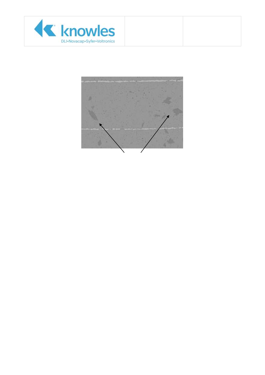
Application Note
Reference No: AN0016
Micro-sectioning of
MLCCs Issue 5
Page 6 of 7
composition may vary due to influences from the electrode material (which itself may
be doped with a ceramic material as a shrinkage aid), but will also be present in the
insulation layers and margins.
Examples of ‘dendrites’
in X7R
Where present, these structural abnormalities do not affect electrical performance of
the components in any way. Product reliability is also unaffected.
Depending on their exact composition, structural abnormalities may be of a slightly
different density (typically higher density) than the general ceramic structure. This
density difference makes the abnormal areas more susceptible to pull out during micro
sectioning, often resulting in the misdiagnosis of a void.
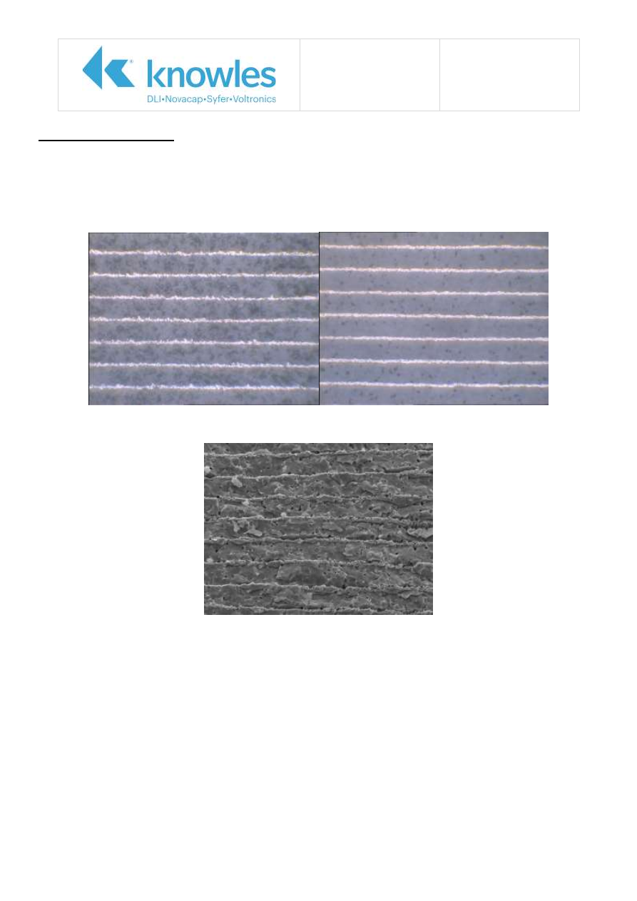
Application Note
Reference No: AN0016
Micro-sectioning of
MLCCs Issue 5
Page 7 of 7
Ceramic Grain Size
Some dielectric materials (particularly COG) may have a large fired grain size. These
materials are especially difficult to micro section, as they virtually impossible to grind
and polish without causing pullout of grains, which being relatively large, will always
appear as voids within the dielectric structure. These materials require extra fine
grinding and careful polishing when preparing sections and it is particularly
recommended that fracture sections are used to verify structure.
Large grained material
Large grained material
Poorly prepared section
Good quality section
Large grained material
Fracture Section SEM Image
AN0018 Issue 4 EMI Suppression using X2Y Components
CN# P109825
EMI Suppression for DC Motors
using X2Y Integrated Passive
Components
Knowles (UK) Limited,
Old Stoke Road, Arminghall, Norwich,
Norfolk, NR14 8SQ, United Kingdom
Tel: +44 (0) 1603 723300
Tel. (Sales): 01603 723310
Fax: +44 (0) 1603 723301
www.knowlescapacitors.com/syfer
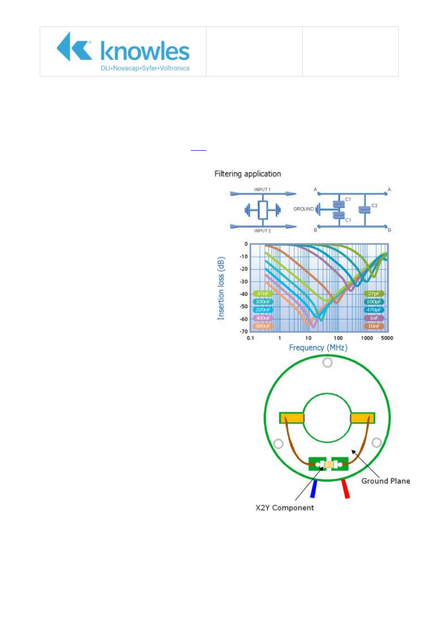
Application Note
Reference No: AN0018
EMI Suppression for DC
Motors using X2Y
Components Issue 4
Page 2 of 3
Introduction
X2Y products are integrated passive components which are manufactured by Syfer Technology Ltd
under license from X2Y Attenuators LLC. For unbalanced applications they provide ultra low ESL
(equivalent series inductance) and are capable of replacing two or more conventional devices.
In order to achieve the ultimate filtering performance the guidelines laid out below should be
considered. Syfer’s X2Y range can be found
Product Selection
When selecting an X2Y component for use in a
DC motor the first thing to consider is the
filtering frequency requirement. Generally for
motors the higher capacitance values are most
suitable.
The graph to the right shows the insertion loss
characteristics for X2Y product, one
consideration is the frequency at which the
maximum performance is required.
MLCCs are susceptible to mechanical cracking
generally as a result of poor processing during
the PCB assembly process. Bending of the PCB
post population is the most common cause.
Because of this issue Flexicap™ Termination is
recommended for capacitors used in motor
applications. Flexicap™ is a polymer based
termination material which is flexible and
absorbs some of the mechanical stress which
may otherwise be exerted on the ceramic
component of the capacitor. Good process
control is still required to completely prevent the
occurrence of mechanical cracking.
Grounding
The grounding of the X2Y component is very important to
the functionality; both ground terminations must be
soldered and the ground should be continuous, as large as
possible and connected to the motor housing at multiple
points.
Placement
The ideal placement for the component is between and
near to the power lines, and as close to the exit point of
the casing as possible. This reduces the incidence of
radiated noise being coupled back on to the lines and
carried out of the casing.
Lead Lengths
Lead lengths both to the brushes and to the X2Y component should be kept a short as possible. This
will reduce the impedance of the path to ground for the noise and will also reduce the incidence of
radiated noise being coupled back on to the lines and carried out of the casing. The track to the solder
tabs should also be as short and as wide as is practical.
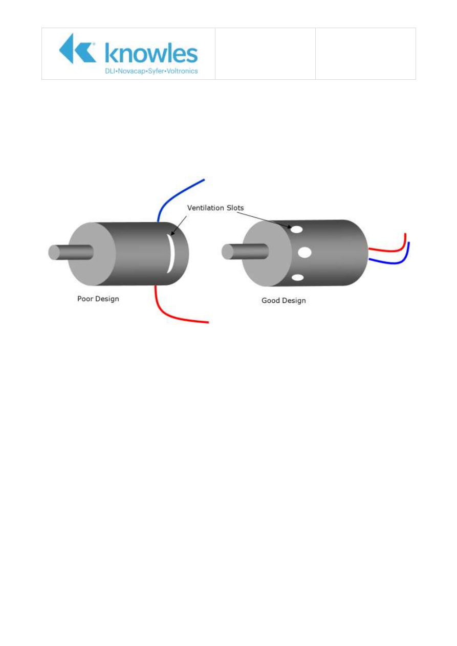
Application Note
Reference No: AN0018
EMI Suppression for DC
Motors using X2Y
Components Issue 4
Page 3 of 3
Housing Design
The motor housing and end cap should ideally be constructed from metal as they act as a
Faraday cage. In the event that this is not possible then maximum metallization should be
used.
The ventilation slots should be round in shape, not rectangular, and be positioned away
from the vicinity of the brushes; this restricts the radiation of noise from the brushes.
The power leads should exit the motor housing in close proximity to each other.

AN0019 Issue 5 – Tin Whiskers - Syfer Surface Mount Capacitors
CN# P109825
Tin Whiskers
Syfer Surface Mount Capacitors
Syfer Surface Mount Terminations ..............................................................2
Syfer Terminations Available .....................................................................3
Part Number Construction .........................................................................4
Syfer 100% Tin Termination Whisker Tests .................................................5
Tin Whisker Tests .................................................................................5
Termination Tin Whisker Inspection.........................................................5
Whisker Test Summary..........................................................................6
Appendix 1 – SEM Images .........................................................................7
Knowles (UK) Limited,
Old Stoke Road, Arminghall, Norwich,
Norfolk, NR14 8SQ, United Kingdom
Tel: +44 (0) 1603 723300
Tel. (Sales): 01603 723310
Fax: +44 (0) 1603 723301
www.knowlescapacitors.com/syfer
Application Note
Reference No: AN0019
Tin Whiskers - Syfer
Surface Mount
Capacitors Issue 5
Page 2 of 8
Introduction
With the implementation of legislation such as the EU RoHS directive prohibiting Lead (Pb) from many
applications there has been a growing concern within the electronics industry that there is an increased
risk of Tin whisker formations causing equipment failure.
Tin whiskers are filaments of Tin that form/ emanate from a pure Tin or plated Tin surface with the
potential reliability risk that a Tin whisker may create a short circuit or an intermittent equipment
failure. Information available on NASA website
http://nepp.nasa.gov/whisker/failures/index.htm
includes some of the equipment failures attributed to Tin whiskers and also provides photographs of
Tin whiskers.
Extensive work has been conducted, for example by NASA and iNEMI (International Electronics
Manufacturing Initiative) into understanding causes for Tin whisker formation. It is believed that
stresses within the Tin such as from intermetallic formations, oxidisation/ corrosion, thermal stress
(temperature cycling) and/ or mechanical stress may contribute to Tin whisker formation.
iNEMI has been involved in Tin whisker research since 2001 and provides recommendations on Lead-
free finishes. For example, 100% Tin plated surface mount capacitors manufactured by Syfer (matte
Tin with Nickel underplate, ceramic capacitors with no leadframe) have been classified by iNEMI as
category 1 (no Tin whisker testing required) or 2 (finish must pass Tin whisker testing). iNEMI category
3 (do not accept this finish in any case) including Tin copper and bright Tin are not manufactured by
Syfer.
http://www.inemi.org/cms/newsroom/PR/2006/PR121506.html
In addition to this, there are several stress tests recommended by, for example, JEDEC (refer to JEDEC
JESD22A121 available at
) and AEC (refer to AEC-Q200 available at
). Note: The tests are recommended tests and are not provided as qualification
tests.
Syfer Surface Mount Terminations
When reviewing Tin whisker information it is often stated that component manufacturers have changed
component plated finishes from Tin/ Lead to 100% Tin in response to legislation such as the EU RoHS
directive. This statement is not true for Syfer capacitors; there has been no change from Tin/ Lead to
100% Tin plating on surface mount components. Syfer has supplied 100% Tin plated components to
customers for many years.
However, in response to customer demand, Syfer has increased the Lead content in Tin/ Lead plated
components to a minimum of 10% Lead.
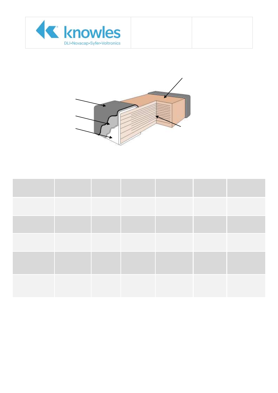
Application Note
Reference No: AN0019
Tin Whiskers - Syfer
Surface Mount
Capacitors Issue 5
Page 3 of 8
Syfer Terminations Available
Table 1 – Syfer Terminations
Termination
Description
Syfer Part
Code
Base Layer Middle Plated
Layer
Top Plated
Layer
RoHS
Compliant?
iNEMI Tin
Whisker Test
Category
Silver Palladium
F
Silver
Palladium
Not
applicable
Not applicable
Yes
Not required,
no Tin finish
Nickel Barrier
with Tin/ Lead
Plating
A
Silver base
Nickel
Tin/Lead with
minimum 10%
Lead
No
Not required,
Lead present in
top layer
Nickel Barrier
with 100% Matte
Tin Plating
J
Silver base
Nickel
100% Matte
Tin
Yes
1 or 2
(1)
FlexiCap™,
Nickel Barrier
with Tin/ Lead
Plating
H
Silver base
Nickel
Tin/Lead with
minimum 10%
Lead
No
Not required,
Lead present in
top layer
FlexiCap
™
, Nickel
Barrier with
100% Matte Tin
Plating
Y
Silver base
Nickel
100% Matte
Tin
Yes
1 or 2
(1)
Notes:
(1) Category 1: No Tin whisker testing required.
Category 2: Finish must pass Tin whisker testing.
iNEMI explains that both categories have been assigned because in general Tin whisker tests are
required but many users have accepted small discrete capacitors with matte Tin over Nickel for
many years. Small discrete capacitors are exceptions to the Tin whisker test requirement
providing certain criteria are met.
Ceramic material
Electrodes
Figure 1 - Capacitor construction diagram
Top layer. Plated with Tin/
Lead or 100% Tin.
Middle layer. Plated Nickel
barrier layer.
Base layer. Either Silver
(sintered) or FlexiCap™

Application Note
Reference No: AN0019
Tin Whiskers - Syfer
Surface Mount
Capacitors Issue 5
Page 4 of 8
Part Number Construction
Example: 1210Y1000103JDT
1210
Y
100
0103
J
D
T
Chip Size
Termination
Voltage d.c.
(marking code)
Capacitance in Pico
farads (pF)
Capacitance
Tolerance
Dielectric
Codes
Packaging
Suffix Code
0603
0805
1206
1210
1808
1812
1825
2220
2225
3640
5550
8060
Y
= FlexiCap
TM
termination base with
nickel barrier (100%
matte tin plating).
RoHS compliant.
H
= FlexiCap
TM
termination base with
nickel barrier (tin/lead
plating with min. 10%
lead).
Not RoHS compliant.
F
= Silver Palladium.
RoHS compliant
J
= Silver base with
nickel barrier (100%
matte tin plating).
RoHS compliant
A
= Silver base with
nickel barrier (tin/lead
plating with min. 10%
lead).
Not RoHS compliant
010
= 10V
016
= 16V
025
= 25V
050
= 50V
063
= 63V
100
= 100V
200
= 200V
250
= 250V
500
= 500V
630
= 630V
1K0
= 1kV
1K2
=1.2kV
1K5
=1.5kV
2K0
= 2kV
2K5
=2.5kV
3K0
=3kV
4K0
=4kV
5K0
=5kV
6K0
=6kV
8K0
=8kV
10K
=10kV
12K
=12kV
<1.0pF
Insert a P for the decimal
point as the first character.
e.g.,
P300
= 0.3pF
Values in 0.1pF steps
≥1.0pF & <10pF
Insert a P for the decimal
point as the second
character.
e.g.,
8P20
= 8.2pF
Values are E24 series
≥10pF
First digit is 0.
Second and third digits are
significant figures of
capacitance code.
The fourth digit is the
number of zeros following.
e.g.,
0101
= 100 pF
Values are E12 series
H
: ± 0.05pF
(only available for
values <4.7pF)
<10pF
B
: ± 0.10pF
C
: ± 0.25pF
D
: ± 0.5pF
F
: ± 1.0pF
≥10pF
F
: ± 1%
G
: ± 2%
J
: ± 5%
K
: ± 10%
M
: ± 20%
A
= C0G (1B/NP0
AEC-Q200 qualified)
C
= C0G (1B/NP0
standard
components)
D
= X7R (2R1 with
IECQ-CECC release)
E
= X7R (2R1 AEC-
Q200 qualified)
F
= C0G (1B/NP0
with IECQ-CECC
release)
(1B)
X
= X7R (2R1
standard
components)
(2R1)
P
= X5R
T
= 178mm
(7”) reel
R
= 330mm
(13”) reel
B
= Bulk pack
– tubs or trays
Used for specific
customer
requirements
For questions or quotation please contact Syfer Sales department.
Tin Whisker Mitigation Practices
The following Tin whisker mitigation practices are employed by Syfer:
Matte Tin plating with Nickel underplate.
Tin plating thickness >2µm.
Annealing process after plating for 150ºC for minimum of 2 hours.
No Lead forming or other stress creating operations after plating.
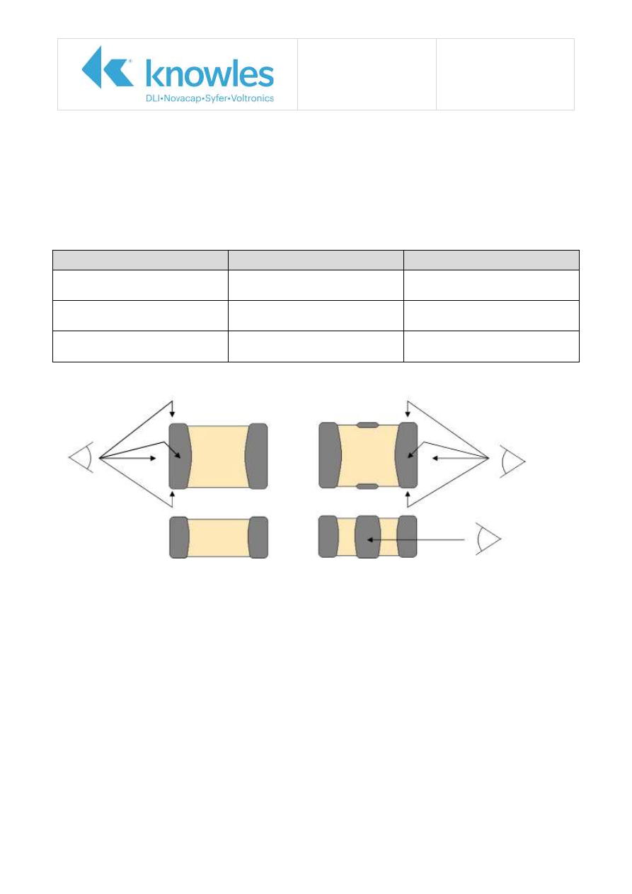
Application Note
Reference No: AN0019
Tin Whiskers - Syfer
Surface Mount
Capacitors Issue 5
Page 5 of 8
Syfer 100% Tin Termination Whisker Tests
In response to general customer enquires regarding Tin whiskers on Syfer 100% Tin plated capacitors,
components have been subjected to the following tests with the purpose of accelerating Tin whisker
growth.
Tin whisker maximum specification (AEC-Q200 section 4.3.4.2): 50µm.
Tin Whisker Tests
Table 2 - Tin Whisker Growth Tests
Stress Type
Test Conditions
Minimum Duration
Temperature Cycling
Tmin: -55ºC
Tmax: +125ºC
1000 cycles
Ambient Temperature/
Humidity Storage
30ºC
60%RH
3000 hours with 1000 hour
inspection intervals
High Temperature/ Humidity
Storage
60ºC
87%RH
3000 hours with 1000 hour
inspection intervals
Termination Tin Whisker Inspection
Figure 2 - Diagrams showing 2 terminal and 3 terminal components
Inspection conducted using optical microscope with 50x to 500x magnification and SEM (Scanning
Electron Microscope) with minimum of 250x magnification. All termination tops and sides examined for
Tin whiskers.
Application Note
Reference No: AN0019
Tin Whiskers - Syfer
Surface Mount
Capacitors Issue 5
Page 6 of 8
Whisker Test Summary
Table 3 – Syfer Capacitor Test Results (Nickel Barrier with 100% Matte Tin Plating)
Capacitor Case
Size
Sample Size
Tin Whisker Test Result
Appendix 1
SEM Photo
Ref
Number of
components
Number of
Terminations
Temp Cycle
30ºC
60%RH
60ºC
87%RH
0603
(2 terminals)
18
36
Pass
No whiskers
Pass
No whiskers
Pass
No whiskers
1
0805
(2 terminals)
9
18
Pass
No whiskers
Pass
No whiskers
Pass
No whiskers
2
0805
(3 terminals)
18
72
Pass
No whiskers
Pass
No whiskers
Pass
No whiskers
3, 4
1206
(3 terminals)
9
36
Pass
No whiskers
Pass
No whiskers
Pass
No whiskers
5, 6
1410
(3 terminals)
18
72
Pass
No whiskers
Pass
No whiskers
Pass
No whiskers
7, 8
1806
(3 terminals)
18
72
Pass
No whiskers
Pass
No whiskers
Pass
No whiskers
9
1812
(2 terminals)
9
18
Pass
No whiskers
Pass
No whiskers
Pass
No whiskers
10
1812
(3 terminals)
18
72
Pass
No whiskers
Pass
No whiskers
Pass
No whiskers
11, 12
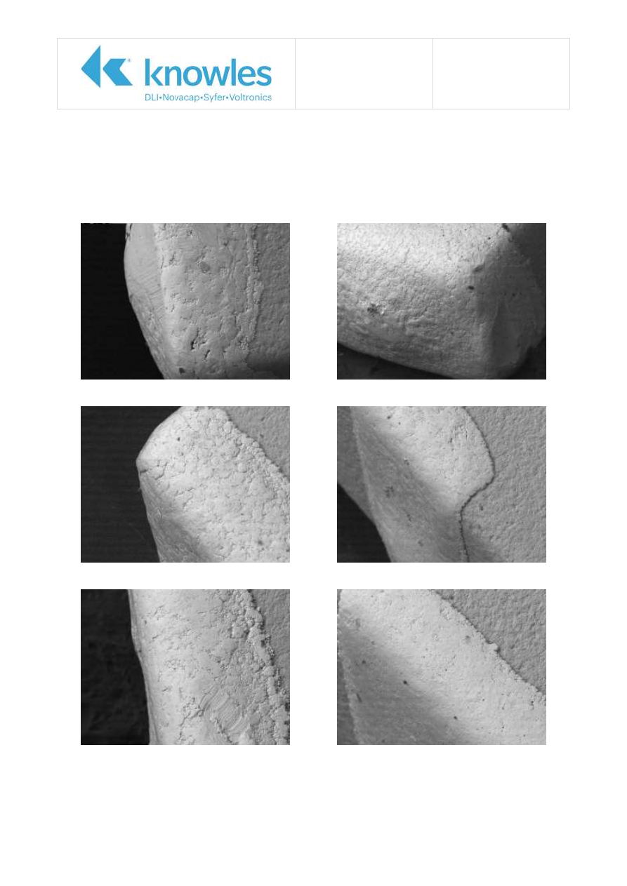
Application Note
Reference No: AN0019
Tin Whiskers - Syfer
Surface Mount
Capacitors Issue 5
Page 7 of 8
Appendix 1 – SEM Images
The following images have been taken using a SEM (Scanning Electron Microscope) after the Tin
whisker tests and are representative of the terminations examined.
Ref 1: 2 terminal 0603
Ref 2: 2 terminal 0805
Ref 3: 3 terminal 0805 - end termination
Ref 4: Side termination
Ref 5: 3 terminal 1206 -end termination
Ref 6: Side termination
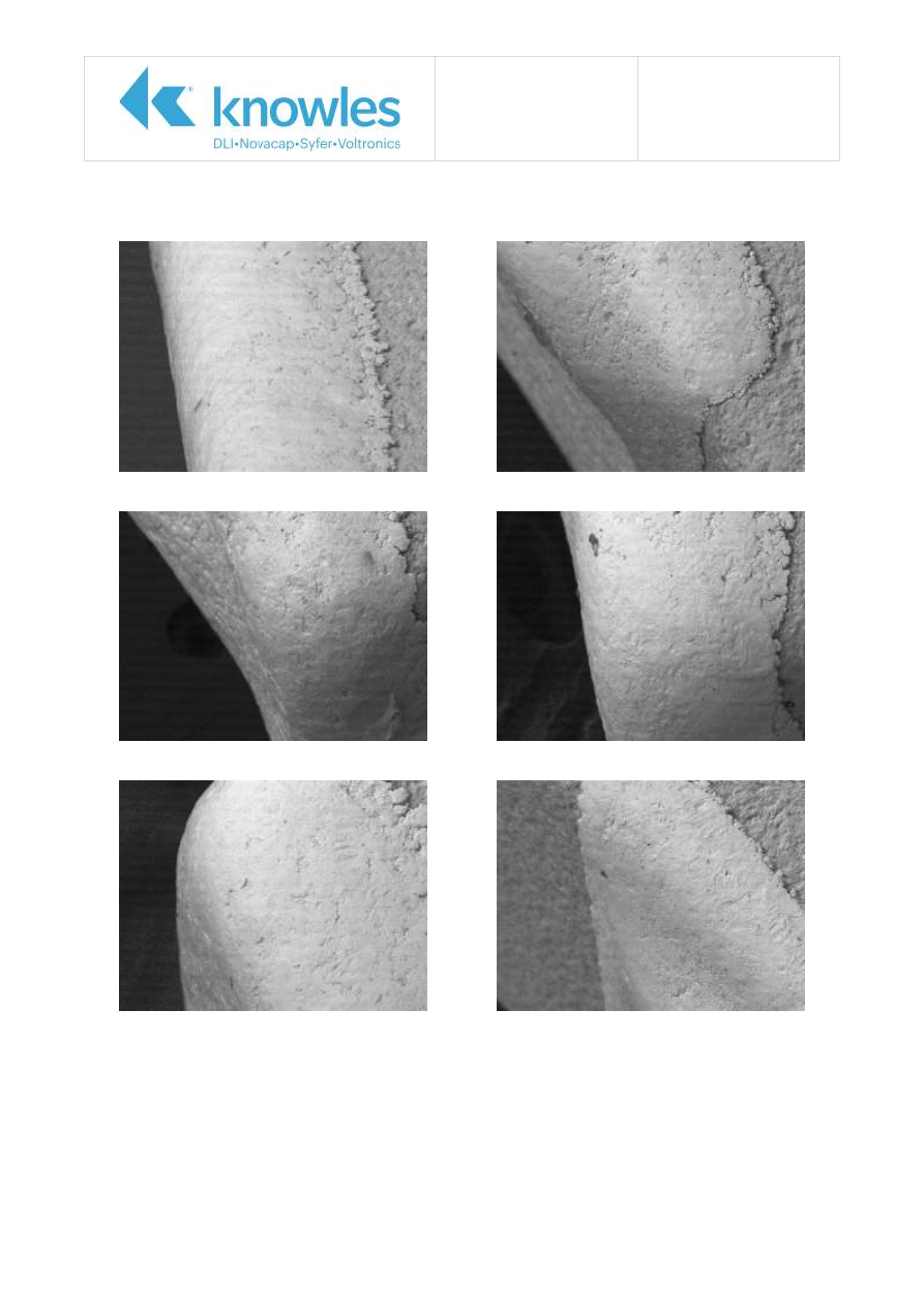
Application Note
Reference No: AN0019
Tin Whiskers - Syfer
Surface Mount
Capacitors Issue 5
Page 8 of 8
Ref 7: 3 terminal 1410 - end termination
Ref 8: Side termination
Ref 9: 3 terminal 1806 - end termination
Ref 10: 2 terminal 1812
Ref 11: 3 terminal 1812 – end termination Ref 12: Side termination

AN0021 Issue 4 – Tandem Capacitors
CN# P109825
Tandem Capacitors
Tandem Capacitors have been designed as a fail safe range using a series section internal design, for
use in any application where short circuits would be unacceptable. When combined with Syfer
FlexiCap™ Termination, Syfer Tandem Capacitors provide an ultra robust and reliable component, for
use in the most demanding applications.
Tandem Capacitors and FlexiCap™ - Product Qualification .............................3
Mechanical Crack Prevention – Syfer Product Group .....................................5
Knowles (UK) Limited,
Old Stoke Road, Arminghall, Norwich,
Norfolk, NR14 8SQ, United Kingdom
Tel: +44 (0) 1603 723300
Tel. (Sales): 01603 723310
Fax: +44 (0) 1603 723301
www.knowlescapacitors.com/syfer
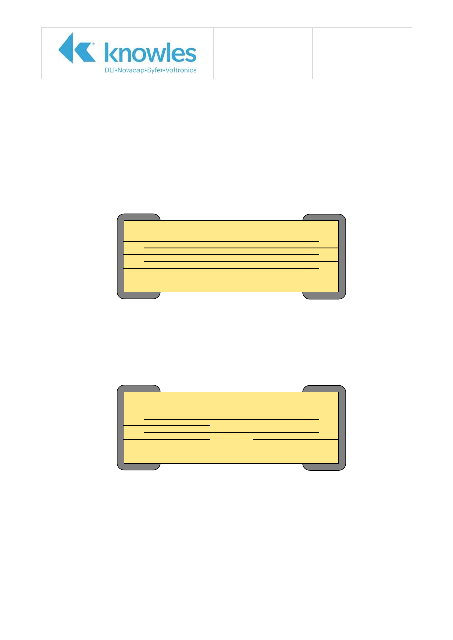
Application Note
Reference No: AN0021
Tandem Capacitors
Issue 4
Page 2 of 6
Introduction
Tandem Capacitors have been designed as a fail safe range using a series section internal design, for
use in any application where short circuits would be unacceptable. A single Tandem capacitor can also
be used in applications where two capacitors placed in series are specified, reducing board space and
assembly time.
The series section design offers the additional benefit of improved ESD performance.
When combined with Syfer FlexiCap™ Termination, Syfer Tandem Capacitors provide an ultra robust
and reliable component, for use in the most demanding applications.
Background
Standard capacitors normally use a single section internal design as shown below.
Example 1 - 200V rated capacitor, Standard Design
In the case of short circuit failure of this type of component, the capacitor would no longer function,
and the circuit would be at risk.
Syfer Tandem capacitors use a series section internal design, where each section is capable of
withstanding the full rated voltage (DWV) of the component as shown below.
Example 2 – 200V rated Tandem capacitor design
NB
- Each section of the tandem capacitor has only 50% of the rated voltage (DWV) applied during
normal use, so the component is under a low stress condition.
200V
0V
Cap 1
Cap 2
100V
100V
200V
0V
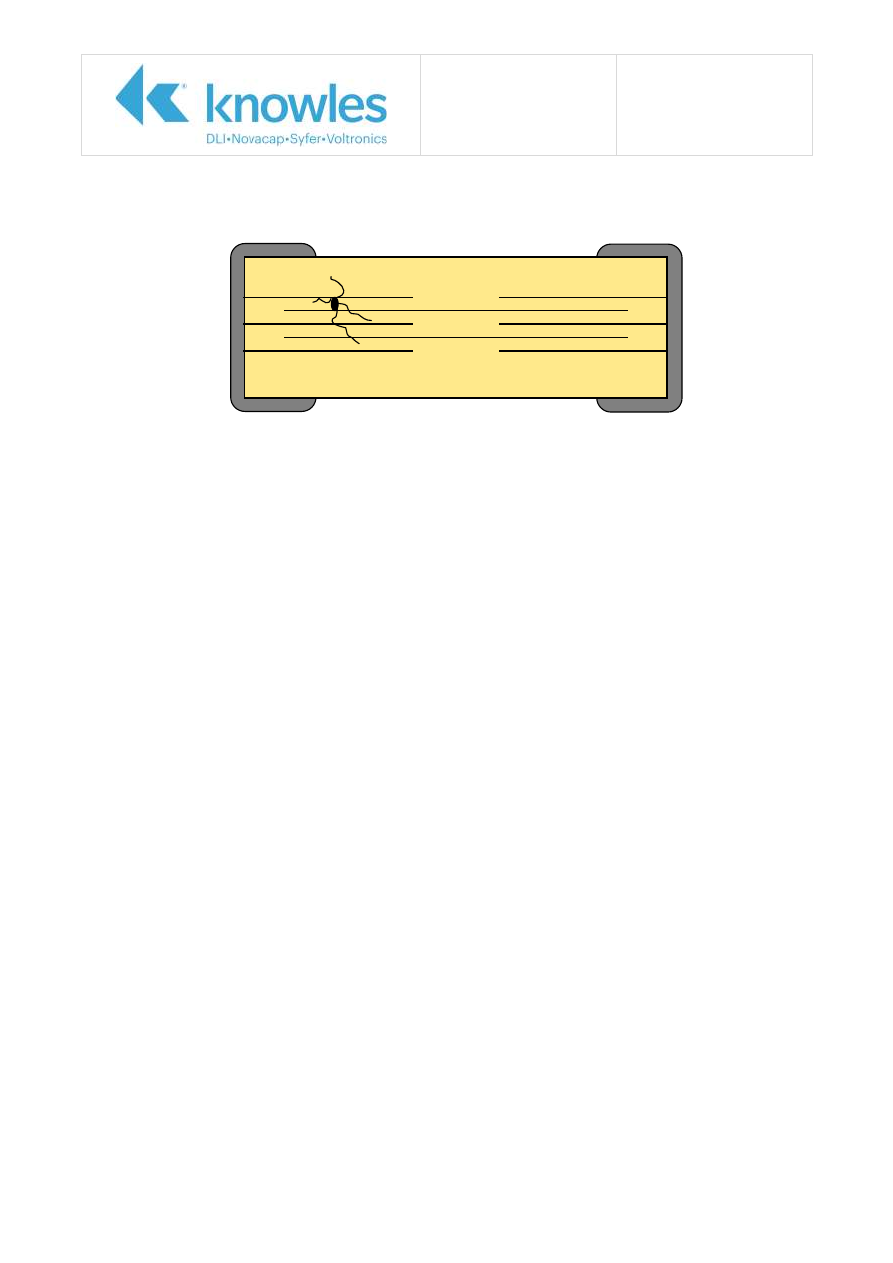
Application Note
Reference No: AN0021
Tandem Capacitors
Issue 4
Page 3 of 6
In the event of a tandem capacitor failing due to short circuit, the second capacitor is capable of
withstanding the resulting doubling in Voltage as shown in the example below.
The left hand capacitor failed due to short circuit, but the right hand capacitor would continue to
function as a normal capacitor, although the component capacitance would change depending on
failure mechanism
.
Tandem Capacitors and FlexiCap™ - Product Qualification
Syfer have built an excellent reputation throughout the industry using FlexiCap™
termination.
FlexiCap™
is proven to prevent failures due to mechanical cracking during the board assembly process.
By combining Tandem Capacitors and FlexiCap™, an ultra-safe range of capacitors has been
introduced, which offers all the benefits of FlexiCap™
,
plus the advantage of two capacitors in series.
Although it is extremely unlikely that a Syfer Capacitor with FlexiCap™ would suffer from mechanical
cracking, under extreme handling conditions, a crack may be formed.
In order to simulate customer use of a cracked component, Tandem Capacitors were manufactured
with Syfer FlexiCap™ termination. Samples were submitted for bend testing in accordance with AECQ-
200 Rev C, in order to crack the components prior to Endurance and 8585 testing of the cracked parts.
It should be noted that in most cases, the FlexiCap™ parts were found to be unbreakable
using a single bend test (up to 10mm of bend), and it was necessary to undertake multiple
bend tests, or to terminate parts using an alternative material in order to break the
components.
Following 1000 hour endurance and 8585 testing, the cracked components were electrically tested, and
then removed from the test boards and microsectioned. Some of the components had lower
capacitance post test, capacitance loss was between zero and 50%, depending on the position of the
cracks (although higher capacitance would be possible for failed Tandem capacitors with failures on
one side of the component).
There were no failures due to short circuit
– i.e. during product qualification it has been
demonstrated that cracked Syfer Tandem Capacitors can be used without risk of failure due
to short circuit.
200V
0V
Cap 1
Cap 2
200V
200V
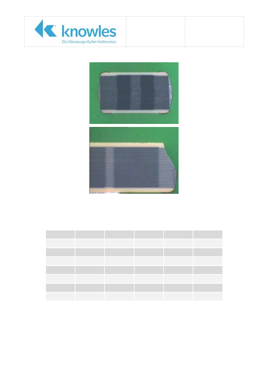
Application Note
Reference No: AN0021
Tandem Capacitors
Issue 4
Page 4 of 6
Examples of Syfer Tandem Capacitors pre and post test
Product Range
Tandem capacitor range is offered in low to mid range capacitance values in X7R dielectric with
FlexiCap™ termination:
Max capacitance in nF (X7R only)
Chip Size
16V
25V
50/63V
100V
200/250V
0603
12
10
6.8
2.2
1.0
0805
47
39
33
10
4.7
1206
150
120
100
47
22
1210
270
220
180
82
47
1812
560
470
390
220
100
2220
1200
1000
680
470
220
2225
1500
1200
1000
680
330
Benefits
Series section internal design provides two capacitors, both capable of independently
working at rated voltage (DWV).
Fully functioning component works at 50% of the applied voltage, resulting in a lower
stress condition.
Tandem Capacitor post
bend and life test.
Capacitance loss
approximately 50%.
NB - Capacitor still
Functioning
Tandem Capacitor
Untested
Application Note
Reference No: AN0021
Tandem Capacitors
Issue 4
Page 5 of 6
Tand
em
cap
Spa
ce
Gra
de
Open Mode
FlexiCap™
Capacitors
Standard FlexiCap™
Components
Standard MLC Capacitor
Tandem
FlexiCap™
Capacitors
Syfer
FlexiCap™ provides protection from mechanical cracking.
Improved ESD performance.
Where two series capacitors are specified, board space and assembly time can be
reduced.
In the event of short circuit failure, one of the two capacitors will continue to function
(although capacitance may be affected).
Available in a wide range of chip sizes and voltage ratings.
Mechanical Crack Prevention – Syfer Product Group
The Tandem Capacitor range is offered to compliment the Syfer standard FlexiCap™ range
and the new Open mode capacitor range, to offer the best possible protection against
mechanical cracking:
High Reliability
Standard
Reliability

Application Note
Reference No: AN0021
Tandem Capacitors
Issue 4
Page 6 of 6
Ordering Information
The Tandem Capacitors can be ordered by using a standard Syfer product code with the suffix code
T01.
Examples:
1206Y0500104KXT
T01
1206Y0500104KET
T01
1206 Case Size
Y
Polymer Termination FlexiCap™
050
50V DC Rated
0104 100nF Capacitance Value
K
10% Capacitance Tolerance
X or E X - X7R Dielectric (standard)
E - X7R Dielectric (AEC-Q200 product)
T
Taped and Reeled
T01 Syfer Tandem Capacitor
All other specifications and properties are as Syfer standard product.
For further information or technical assistance please contact our Sales Department on +44 1603
723310 or by Email at

AN0022 Issue 5 – Open Mode Capacitors
CN# P109825
Open Mode Capacitors
Open mode capacitors have been designed using inset electrode margins specifically for use in
applications where mechanical cracking is a severe problem. When combined with Syfer
FlexiCap™ Termination, Syfer Open Mode Capacitors provide a robust component, with the
assurance that if a part becomes cracked, the crack will be unlikely to result in short circuit
failure.
Open mode and FlexiCap™ - Product Qualification .......................................3
Mechanical Crack Prevention – Syfer Product Group .....................................5
Knowles (UK) Limited,
Old Stoke Road, Arminghall, Norwich,
Norfolk, NR14 8SQ, United Kingdom
Tel: +44 (0) 1603 723300
Tel. (Sales): 01603 723310
Fax: +44 (0) 1603 723301
www.knowlescapacitors.com/syfer
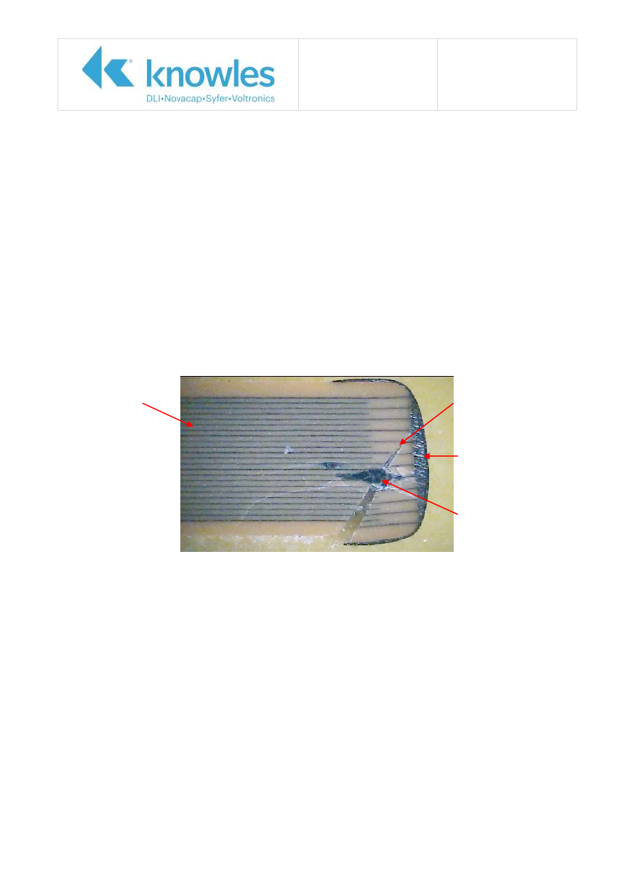
Application Note
Reference No: AN0022
Open Mode Capacitors
Issue 5
Page 2 of 6
Introduction
Open mode Capacitors have been designed specifically for use in applications where mechanical
cracking is a severe problem and short circuits due to cracking are unacceptable. Open mode
capacitors use inset electrode margins, which prevent any mechanical cracks which may form during
board assembly from connecting to the internal electrodes.
When combined with Syfer’s FlexiCap™ Termination, Syfer open mode capacitors provide a robust
component with the assurance that if a part becomes cracked, the crack will be unlikely to result in
short circuit failure.
Background
One of the most common causes of failure with standard capacitors is directly attributable to bending
of the printed circuit board (PCB) after solder attachment. Excessive bending will create mechanical
crack(s) within the ceramic capacitor. Mechanical cracks, depending upon severity, may not cause
capacitor failure during the final assembly test. Over time, moisture penetration into the crack can
cause a reduction in insulation resistance and eventual dielectric breakdown leading to capacitor failure
in service.
Mechanical cracking always initiates from the point of highest stress, which is at the junction of the
ceramic body and the termination band.
Mechanical
Crack
Electrical failure site
Termination Material
Electrodes

Application Note
Reference No: AN0022
Open Mode Capacitors
Issue 5
Page 3 of 6
Syfer open mode capacitors use an inset electrode design which prevents any mechanical crack from
crossing the active area of the capacitor, therefore preventing a short circuit failure as shown below.
Important Notes
Syfer open mode capacitors will only fail as open circuit (or low capacitance) if the failure is due
to mechanical cracking. Any other cause of capacitor failure will almost certainly result in short
circuit.
Syfer strongly recommends the avoidance of any procedure that may generate mechanical
cracking, as a cracked part may in time create degradation and failure. Open mode capacitors
will minimise but cannot completely eliminate this risk.
Open mode and FlexiCap™ - Product Qualification
Syfer have built an excellent reputation throughout the industry using FlexiCap™ termination.
FlexiCa™ is proven to prevent failures due to mechanical cracking during the board assembly process.
By combining Open mode Capacitors and FlexiCap™, a range of capacitors has been introduced which
offers all the benefits of FlexiCap™, plus the advantage of an inset electrode design.
Although it is extremely unlikely that a Syfer Capacitor with FlexiCap™ would suffer from mechanical
cracking, under extreme handling conditions, a crack may be formed.
In order to simulate customer use of a cracked component, Open mode Capacitors were manufactured
with Syfer FlexiCap™ termination. Samples were submitted for bend testing in accordance with AECQ-
200 Rev C, in order to crack the components prior to Endurance and 8585 testing of the cracked parts.
It should be noted that in most cases, the
FlexiCap™ parts were found to be unbreakable
using a single bend test (up to 10mm of bend), and it was necessary to undertake multiple
bend tests, or to terminate parts using an alternative material in order to break the
components.
Following 1000 hour endurance and 8585 testing, the cracked components were electrically tested, and
then removed from the test boards and micro sectioned. Some of the components had lower
capacitance post test, capacitance loss was between zero and 70%, depending on the position of the
cracks. There were no failures due to short circuit detected.
Inset margin
Active area
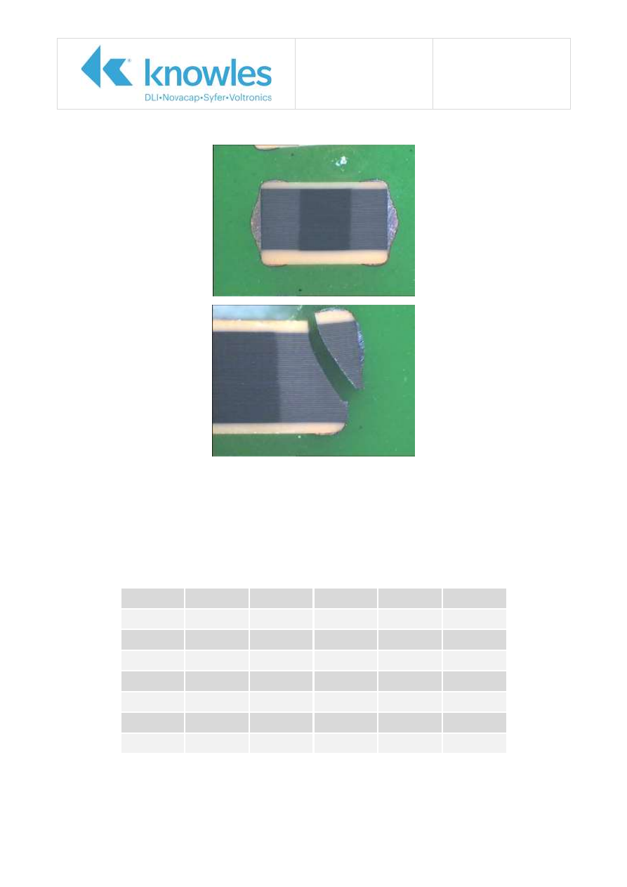
Application Note
Reference No: AN0022
Open Mode Capacitors
Issue 5
Page 4 of 6
Examples of Open Mode Capacitors pre and post test
Product Range
The Open mode capacitor range is offered in low to high range capacitance values in X7R dielectric. It
is recommended only with FlexiCap™ termination, but other termination materials may be available
upon request.
Note
– use of non FlexiCap™ termination will increase the risk of cracks caused by mechanical or
thermal cycling stress.
Max capacitance in nF (X7R only)
Chip size
16V
25V
50/63V
100V
200/250V
0603
39
33
22
6.8
2.7
0805
150
120
100
27
15
1206
470
330
220
100
68
1210
680
560
470
220
100
1812
1500
1200
1000
680
330
2220
3300
2200
1500
1000
680
2225
4700
3900
2700
1800
1000
Other case sizes and voltages may be available on request.
Open Mode Capacitor
post bend and
85˚C/85%RH test.
Capacitance loss
approximately 70%.
NB – Capacitor still
functioning
Open Mode Capacitor
Untested
Application Note
Reference No: AN0022
Open Mode Capacitors
Issue 5
Page 5 of 6
Tand
em
cap
Spa
ce
Gra
de
Standard FlexiCap™ Components
Standard MLC Capacitors
Tandem
FlexiCap™
Capacitors
Open Mode
FlexiCap™
Capacitors
Benefits
Inset electrode design provides protection in case of mechanical cracking, with any crack
formed likely to result in low capacitance or open circuit rather than short circuit failure.
Syfer
FlexiCap™ provides protection from mechanical cracking.
Available in a wide range of chip sizes and voltage ratings
Mechanical Crack Prevention – Syfer Product Group
The Open mode range is offered to compliment the Syfer standard FlexiCap™ range and
the new Tandem capacitor range, to offer the best possible protection against mechanical
cracking:
High Reliability
Standard
Reliability

Application Note
Reference No: AN0022
Open Mode Capacitors
Issue 5
Page 6 of 6
Ordering Information
The Open mode Capacitors can be ordered by using a standard Syfer product code with the suffix code
M01.
Examples:
1206Y0500104KXT
M01
1206Y0500104KET
M01
1206 Case Size
Y
Polymer Termination FlexiCap™
050
50V DC Rated
0104 100nF Capacitance Value
K
10% Capacitance Tolerance
X or E X - X7R Dielectric (standard)
E - X7R dielectric (AEC-Q200 product)
T
Taped and Reeled
M01 Syfer Open mode Capacitor
All other specifications and properties are as Syfer standard product.
For further information or technical assistance please contact our Sales Department on +44 1603
723310 or by Email at

AN0024 Issue 4 -
IPC/JEDEC J-STD-020D
CN# P109825
IPC/JEDEC J-STD-020D
Moisture/Reflow Sensitivity Classification for Non-hermetic Solid State Surface
Mount Devices
Syfer Surface Mount Capacitor Test Results
Introduction .....................................................................................2
Moisture Sensitivity Classification Process ............................................2
Initial Electrical Test ......................................................................2
Initial Visual .................................................................................2
Bake ............................................................................................2
Moisture Soak ...............................................................................2
Reflow x 3 ....................................................................................3
Final External Visual ......................................................................3
Final Electrical Test ........................................................................3
Final Internal Visual Examination ....................................................3
Failure Criteria .................................................................................4
Syfer Test Summary .........................................................................5
Appendix 1 – Capacitor Photographs ...........................................................6
Knowles (UK) Limited,
Old Stoke Road, Arminghall, Norwich,
Norfolk, NR14 8SQ, United Kingdom
Tel: +44 (0) 1603 723300
Tel. (Sales): 01603 723310
Fax: +44 (0) 1603 723301
www.knowlescapacitors.com/syfer
Application Note
Reference No: AN0024
IPC/JEDEC J-STD-020D
Issue 4
Page 2 of 8
1.0 Introduction
The purpose of J-STD-020 is to identify the moisture sensitivity classification level of non-hermetic
solid state surface mount devices (SMDs). The classification level
enables proper packaging, storage
and handled to prevent potential damage as a result of moisture-induced stress during soldering
operations and/ or repair operations.
Moisture Sensitivity Levels defined by J-STD-020
Level
Floor Life
Time
Condition
1
(1)
Unlimited
(2)
≤30ºC/ 85%RH
2
1 year
≤30ºC/ 60%RH
2a
4 weeks
≤30ºC/ 60%RH
3
168 hours
≤30ºC/ 60%RH
4
72 hours
≤30ºC/ 60%RH
5
48 hours
≤30ºC/ 60%RH
5a
24 hours
≤30ºC/ 60%RH
6
Time On Label (TOL)
≤30ºC/ 60%RH
Notes:
(1) If a device passes level 1, it is classified as not being moisture sensitive and does not require dry
pack.
(2) Unlimited floor life refers specifically to moisture sensitivity related to components cracking during
soldering operations. Other factors may affect, for example, component solderability. Syfer
recommended shelf life and storage conditions are available at
www.knowlescapacitors.com/syfer
Copies of J-STD-020 are available at
2.0 Moisture Sensitivity Classification Process
2.1
Initial Electrical Test
Capacitors tested for:
Capacitance.
Dissipation Factor.
Insulation resistance.
Dielectric Withstand Voltage.
2.2
Initial Visual
Capacitors externally visually examined using 50x magnification.
2.3
Bake
Capacitors subjected to minimum 24hours at 125ºC +5/-0ºC.
2.4
Moisture Soak
Capacitors placed in a humidity chamber at 85ºC/ 85%RH for 168 hours.
Application Note
Reference No: AN0024
IPC/JEDEC J-STD-020D
Issue 4
Page 3 of 8
2.5
Reflow x 3
Within 15 minutes to maximum 4 hours after the moisture soak, capacitors subjected to 3x
reflow soldering profile.
Reflow soldering profile used by Syfer:
2.6
Final External Visual
Capacitors externally visually examined using 50x magnification.
2.7
Final Electrical Test
Capacitors tested for:
Capacitance
Dissipation Factor
Insulation resistance
Dielectric Withstand Voltage
2.8
Final Internal Visual Examination
J-STD-020 includes a final acoustic microscopy stage after the final electrical test with any
component identified with a crack being evaluated by sectioning.
Application Note
Reference No: AN0024
IPC/JEDEC J-STD-020D
Issue 4
Page 4 of 8
Acoustic microscopy may not identify all cracks within capacitors and to verify that no cracks
are present, Syfer has sectioned all capacitors tested.
Sectioning is conducted by mounting capacitors in high edge retention potting compound and
then grinding through the capacitors. During the grinding process, the capacitors have been
frequently examined using up to 200x magnification checking for cracks.
3.0 Failure Criteria
If 1 or more capacitor in the test sample fails then the whole family group is considered to have failed
the tested MSL (Moisture Sensitivity Level).
A capacitor is considered to have failed if it exhibits any of the following after the 168 hour moisture
soak and subsequent 3x reflow processes:
Crack observed during the Final External Visual examination
Final Electrical Test failure
Crack observed during the Final Internal Visual examination
Electrode
s
Figure 1 - Capacitor construction diagram
Top layer. Plated with
either Tin/ Lead or 100%
Tin.
Middle layer. Plated Nickel
barrier layer.
Base layer. Either Silver
(sintered) or FlexiCap™
Ceramic material
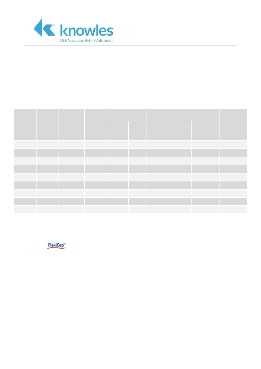
Application Note
Reference No: AN0024
IPC/JEDEC J-STD-020D
Issue 4
Page 5 of 8
4.0 Syfer Test Summary
Moisture/ reflow sensitivity classification has been conducted by Syfer based on a family sampling
approach in relation to:
Capacitor case size
Dielectric classification
Termination type
Results
Capacitor
Case Size
Dielectric
Type
Termination
Type
(1)
Sample
Size
Pre Moisture Soak
and 3x Reflow
Post Moisture Soak/
3x Reflow
Appendix 1
Photo Ref
2.1 Initial
Electrical
Tests
2.2
Initial
Visual
2.6 Final
External
Visual
2.7 Final
Electrical
Tests
2.8 Internal
Visual
Examination
0603
C0G
J
25
Pass
Pass
Pass
Pass
Pass
1 and 2
0603
X7R
J
25
Pass
Pass
Pass
Pass
Pass
3 and 4
0603
X7R
Y
25
Pass
Pass
Pass
Pass
Pass
5 and 6
1210
C0G
J
25
Pass
Pass
Pass
Pass
Pass
7 and 8
1210
X7R
J
25
Pass
Pass
Pass
Pass
Pass
9 and 10
1210
X7R
Y
25
Pass
Pass
Pass
Pass
Pass
11 and 12
2225
C0G
J
25
Pass
Pass
Pass
Pass
Pass
13 and 14
2225
X7R
J
25
Pass
Pass
Pass
Pass
Pass
15 and 16
2225
X7R
Y
25
Pass
Pass
Pass
Pass
Pass
17 and 18
Notes:
(1) Termination type refers to the code letter used in Syfer part numbers.
J:
Silver base with Nickel Barrier
(100% matte tin Plating).
Y:
termination base with Ni Barrier (100% matte tin plating).
All capacitors tested passed Moisture Sensitivity Level (MSL) 1 and are not classified as being
moisture sensitive. The capacitors supplied by Syfer do not require dry pack.
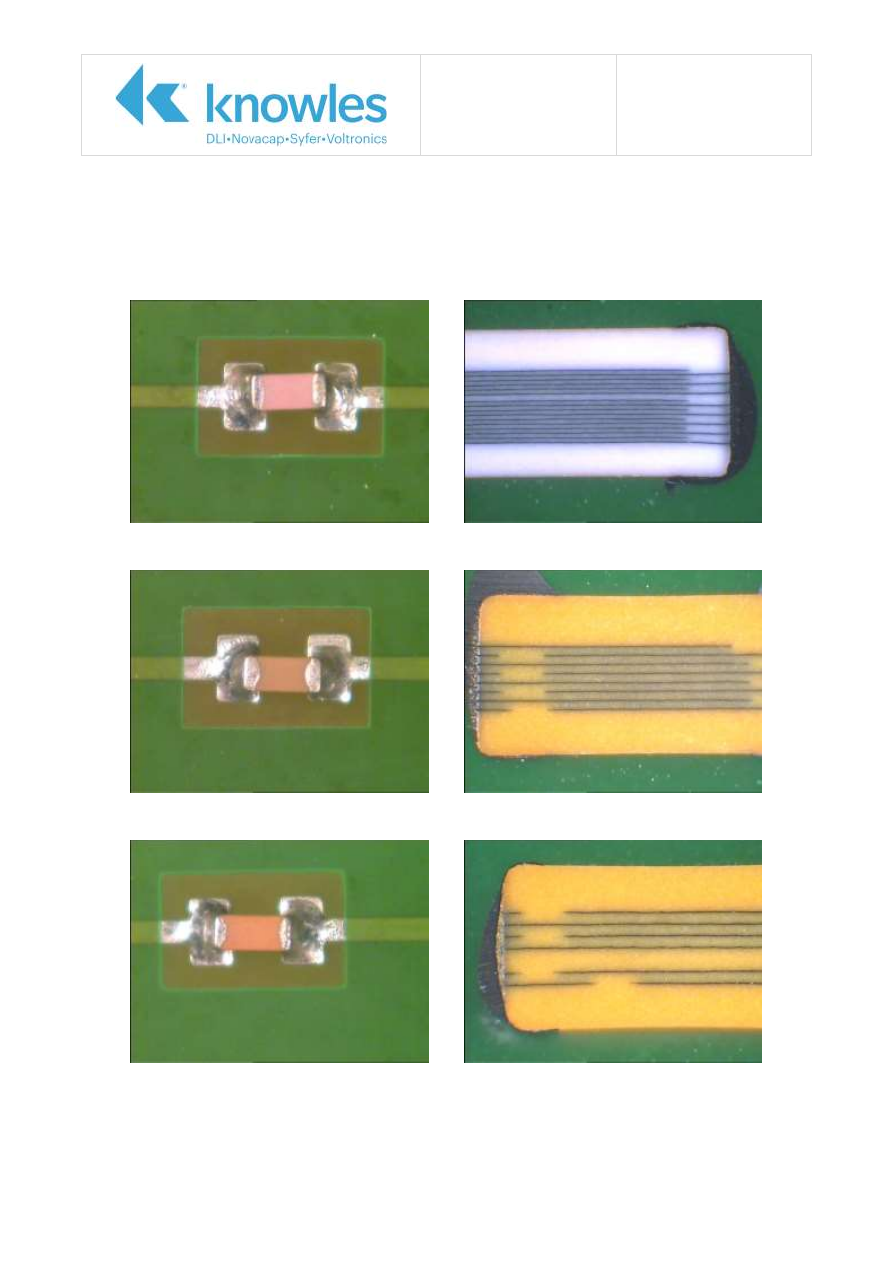
Application Note
Reference No: AN0024
IPC/JEDEC J-STD-020D
Issue 4
Page 6 of 8
Appendix 1 – Capacitor Photographs
The following photographs have been taken after the moisture soak and 3x reflow processes and are
representative of the capacitors subjected to the
moisture/ reflow sensitivity classification tests.
0603 C0G J Termination
Ref 1. Final External Visual
Ref 2. Final Internal Visual (100x mag)
0603 X7R J Termination
Ref 3. Final External Visual
Ref 4. Final Internal Visual (100x mag)
0603 X7R Y Termination
Ref 5. Final External Visual
Ref 6. Final Internal Visual (100x mag)
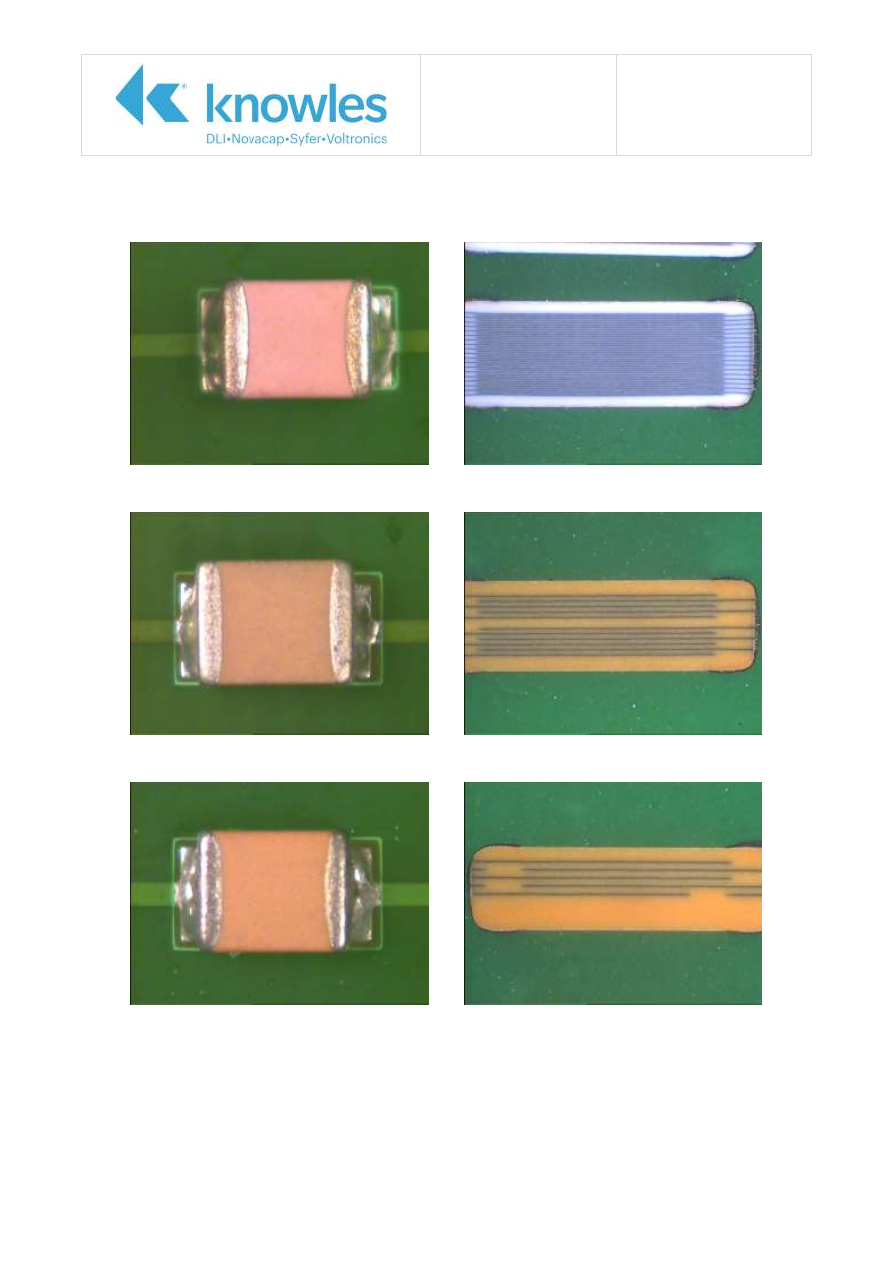
Application Note
Reference No: AN0024
IPC/JEDEC J-STD-020D
Issue 4
Page 7 of 8
1210 C0G J Termination
Ref 7. Final External Visual
Ref 8. Final Internal Visual (50x mag)
1210 X7R J Termination
Ref 9. Final External Visual
Ref 10. Final Internal Visual (50x mag)
1210 X7R Y Termination
Ref 11. Final External Visual
Ref 12. Final Internal Visual (50x mag)
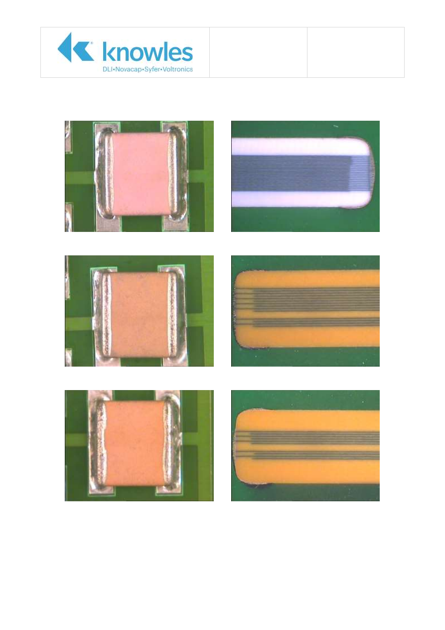
Application Note
Reference No: AN0024
IPC/JEDEC J-STD-020D
Issue 4
Page 8 of 8
2225 C0G J Termination
Ref 13. Final External Visual
Ref 14. Final Internal Visual (50x mag)
2225 X7R J Termination
Ref 15. Final External Visual
Ref 16. Final Internal Visual (50x mag)
2225 X7R Y Termination
Ref 17. Final External Visual
Ref 18. Final Internal Visual (50x mag)

AN0025 Issue 4 – LCD Inverter Range
CN# P109825
LCD Inverter Range - 5kV and 6kV
Surface Mount Capacitors
Knowles (UK) Limited,
Old Stoke Road, Arminghall, Norwich,
Norfolk, NR14 8SQ, United Kingdom
Tel: +44 (0) 1603 723300
Tel. (Sales): 01603 723310
Fax: +44 (0) 1603 723301
www.knowlescapacitors.com/syfer
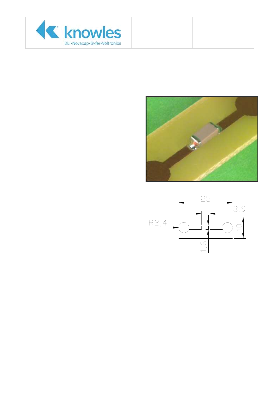
Application Note
Reference No: AN0025
LCD Inverter Range
Issue 4
Page 2 of 3
Introduction
Syfer Technology Ltd has developed a new range of capacitors aimed specifically at the high voltage
LCD inverter market. The requirement is for a surface mountable device which can replace leaded
components used at present. Syfer has produced components in 1808 and 1812 case sizes which are
capable of withstanding greater than 6kV prior to the inception of surface arcing without the need for
conformal coating post soldering. This breakthrough in surface mount technology has been achieved by
the combination of the use of a unique C0G type
dielectric material and the optimisation of physical
and electrical design.
Testing
Testing has been undertaken at Syfer in order to
demonstrate and verify the advantages of the LCD
inverter range over standard X7R and C0G product.
Components were mounted onto FR4 PCB
substrates using SN62A solder with no clean flux
and a reflow soldering process. Testing was
conducted using a Sefelec MPC47P Dielectrimeter
and a Glassman High Voltage power supply, parts
were subjected to Voltage Proof testing at
increasing levels of DC voltage until failure
occurred, failure was considered as a single visible
arc, multiple arcs or dielectric breakdown
Above: Test Board and Dimensions (mm)
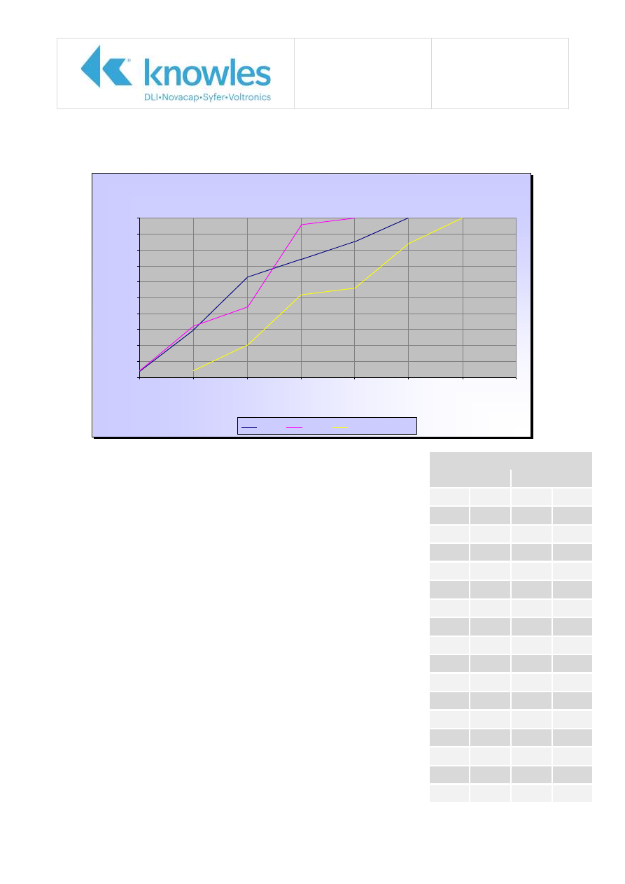
Application Note
Reference No: AN0025
LCD Inverter Range
Issue 4
Page 3 of 3
Results
Testing conducted at approx. 24°C and 30% RH
Results show a significant improvement in performance over Syfer
standard high voltage components manufactured from both X7R and
C0G materials, arcing inception is increased by 500V to 6.5kV and
ultimate performance is improved by up to 1kV.
Conclusion
Whilst standard Syfer 1808 and 1812 high voltage capacitors offer
excellent performance, at voltages of 4kV and greater conformal
coating may be required post soldering in order to ensure that no
surface arcing will occur. The LCD inverter range, variation due to PCB
design and atmospheric conditions accepted, is capable of withstanding
greater than 6kV as supplied, this ability allows for the replacement of
more bulky leaded radial components.
Ordering Information
The LCD inverter range can be ordered using a standard Syfer product
code with the addition of suffix code FB9.
Examples: 1808J6K00150FCT
FB9
or
1812J6K00220GCT
FB9
LCD Inverter Range
1808
1812
5kV
6kV
5kV
6kV
1.5pF 1.5pF 3.9pF 3.9pF
1.8pF 1.8pF 4.7pF 4.7pF
2.2pF 2.2pF 5.6pF 5.6pF
2.7pF 2.7pF 6.8pF 6.8pF
3.3pF 3.3pF 8.2pF 8.2pF
3.9pF 3.9pF 10pF 10pF
4.7pF 4.7pF 12pF 12pF
5.6pF 5.6pF 15pF 15pF
6.8pF 6.8pF 18pF 18pF
8.2pF 8.2pF 22pF 22pF
10pF 10pF 27pF 27pF
12pF 12pF 33pF 33pF
15pF
-
39pF
-
18pF
-
47pF
-
22pF
-
56pF
-
-
-
68pF
-
Cumulative Flash Failures 1808 6kV
0%
10%
20%
30%
40%
50%
60%
70%
80%
90%
100%
6000
6500
7000
7500
8000
8500
9000
9500
Flash Voltage
C
um
ul
a
ti
v
e
Fa
il
ure
s
X7R
C0G
Inverter Range

AN0026 Issue 4 – FlexiCap™ Thermal Out-gassing Test
CN# P109825
ECSS-Q-70-02A
Thermal vacuum outgassing test for
the screening of space materials
Syfer FlexiCap™ Surface Mount Capacitor Test Results
Test Report Abbreviated Terms ..................................................................2
ECSS-Q-70-02A Acceptance Limits .............................................................3
Appendix 1 – Test Laboratory Report ..........................................................4
Knowles (UK) Limited,
Old Stoke Road, Arminghall, Norwich,
Norfolk, NR14 8SQ, United Kingdom
Tel: +44 (0) 1603 723300
Tel. (Sales): 01603 723310
Fax: +44 (0) 1603 723301
www.knowlescapacitors.com/syfer
Application Note
Reference No: AN0026
FlexiCap™ Thermal Out-
gassing Test Issue 4
Page 2 of 16
Introduction
This application note is primarily aimed at Space customers to provide outgassing test data conducted
in accordance with ECSS-Q-70-02A on Syfer’s FlexiCap™ termination material.
FlexiCap™ termination is a proven material that withstands greater levels of mechanical stress when
compared with conventional sintered termination. For example, mechanical stress induced by PCB flex
or temperature cycling.
FlexiCap™ is a silver loaded epoxy polymer that is applied onto the ceramic body of the component
using conventional termination techniques. After the termination process stage the capacitors are
plated with Nickel and Tin or Tin/Lead using the same methods as for the sintered Silver terminated
capacitors.
Many customers have recognized the benefits provided and have approved FlexiCap™ for applications
including high reliability requirements such as automotive, military and aerospace.
For qualification tests conducted on FlexiCap™ terminated capacitors refer to Syfer application notes:
AN0001 available at
www.knowlescapacitors.com/syfer
. This application note provides details
on the FlexiCap™ material, qualification tests conducted and also comparative data with
sintered termination.
AN0009 available at
www.knowlescapacitors.com/syfer
. This application note provides details
on the rigorous AEC-Q200 automotive stress test requirements conducted on X7R capacitors
terminated with FlexiCap™.
Test Laboratory
The test report provided in appendix 1 has been prepared by Intespace located in Toulouse, France.
Intespace is a leading laboratory conducting all types of environmental testing including Space
applications. Further information is available at
The customer information stated on the first page of the Intespace report refers to Alter Technology
Group. The reason for this is that Syfer supplied the material to Alter who then subcontracted the
outgassing test to be conducted by Intespace.
Test Report Abbreviated Terms
CVCM: Collected Volatile Condensable Material
RML: Recovered Mass Loss
TML: Total Mass Loss
WVR: Water Vapour Regained
Application Note
Reference No: AN0026
FlexiCap™ Thermal Out-
gassing Test Issue 4
Page 3 of 16
ECSS-Q-70-02A Acceptance Limits
The following limits are defined in ECSS-Q-70-02A
as general acceptance limits. Note: The acceptance
limits for materials that are used in the fabrication of optical devices or in the vicinity of optical devices
may be more stringent than the general limits stated.
RML: < 1.0 %
CVCM: < 0.10 %
Report Summary
Section 7 titled Results in the report issued by Intespace test laboratory confirms that FlexiCap™
termination material is in compliance with ECSS-Q-70-02A.
Ordering Information
Part Number Construction
Example: 1210H1000103JXT
1210
H
100
0103
J
X
T
Chip Size
Termination
Voltage d.c.
(marking code)
Capacitance in Pico
farads (pF)
Capacitance
Tolerance
Dielectric
Codes
Packaging
Suffix Code
0603
0805
1206
1210
1808
1812
1825
2220
2225
3640
5550
8060
Y
= FlexiCap
TM
termination base with
nickel barrier (100%
matte tin plating).
RoHS compliant.
H
= FlexiCap
TM
termination base with
nickel barrier (tin/lead
plating with min. 10%
lead).
Not RoHS compliant.
010
= 10V
016
= 16V
025
= 25V
050
= 50V
063
= 63V
100
= 100V
200
= 200V
250
= 250V
500
= 500V
630
= 630V
1K0
= 1kV
1K2
=1.2kV
1K5
=1.5kV
2K0
= 2kV
2K5
=2.5kV
3K0
=3kV
4K0
=4kV
5K0
=5kV
6K0
=6kV
8K0
=8kV
10K
=10kV
12K
=12kV
<1.0pF
Insert a P for the decimal
point as the first character.
e.g.,
P300
= 0.3pF
Values in 0.1pF steps
≥1.0pF & <10pF
Insert a P for the decimal
point as the second
character.
e.g.,
8P20
= 8.2pF
Values are E24 series
≥10pF
First digit is 0.
Second and third digits are
significant figures of
capacitance code.
The fourth digit is the
number of zeros following.
e.g.,
0101
= 100 pF
Values are E12 series
H
: ± 0.05pF
(only available for
values <4.7pF)
<10pF
B
: ± 0.10pF
C
: ± 0.25pF
D
: ± 0.5pF
F
: ± 1.0pF
≥10pF
F
: ± 1%
G
: ± 2%
J
: ± 5%
K
: ± 10%
M
: ± 20%
A
= C0G (1B/NP0
AEC-Q200 qualified)
C
= C0G (1B/NP0
standard
components)
D
= X7R (2R1 with
IECQ-CECC release)
E
= X7R (2R1 AEC-
Q200 qualified)
F
= C0G (1B/NP0
with IECQ-CECC
release)
(1B)
X
= X7R (2R1
standard
components)
(2R1)
P
= X5R
T
= 178mm
(7”) reel
R
= 330mm
(13”) reel
B
= Bulk pack
– tubs or trays
Q
= Waffle
pack
Used for specific
customer
requirements
For Space applications, Syfer supplies components to Syfer Detail Specification reference S02A 0100.
This specification has been generated in accordance with ESCC Generic Specification 3009 and
corresponding ESCC component detail specifications.
For further information contact Syfer Sales at
Application Note
Reference No: AN0026
FlexiCap™ Thermal Out-
gassing Test Issue 4
Page 4 of 16
Appendix 1 – Test Laboratory Report
Application Note
Reference No: AN0026
FlexiCap™ Thermal Out-
gassing Test Issue 4
Page 5 of 16
Application Note
Reference No: AN0026
FlexiCap™ Thermal Out-
gassing Test Issue 4
Page 6 of 16
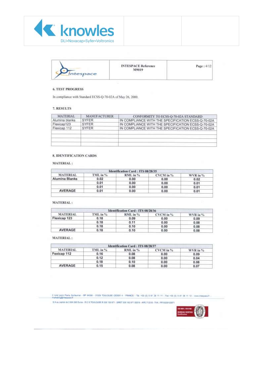
Application Note
Reference No: AN0026
FlexiCap™ Thermal Out-
gassing Test Issue 4
Page 7 of 16
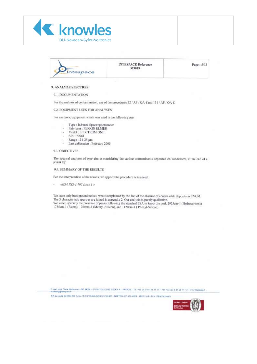
Application Note
Reference No: AN0026
FlexiCap™ Thermal Out-
gassing Test Issue 4
Page 8 of 16
Application Note
Reference No: AN0026
FlexiCap™ Thermal Out-
gassing Test Issue 4
Page 9 of 16
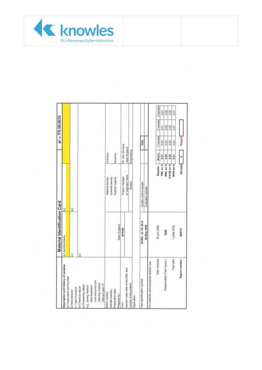
Application Note
Reference No: AN0026
FlexiCap™ Thermal Out-
gassing Test Issue 4
Page 10 of 16
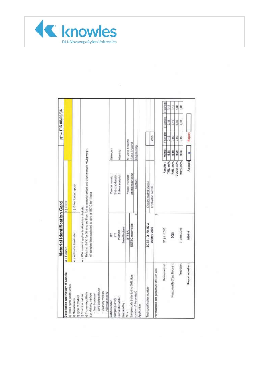
Application Note
Reference No: AN0026
FlexiCap™ Thermal Out-
gassing Test Issue 4
Page 11 of 16
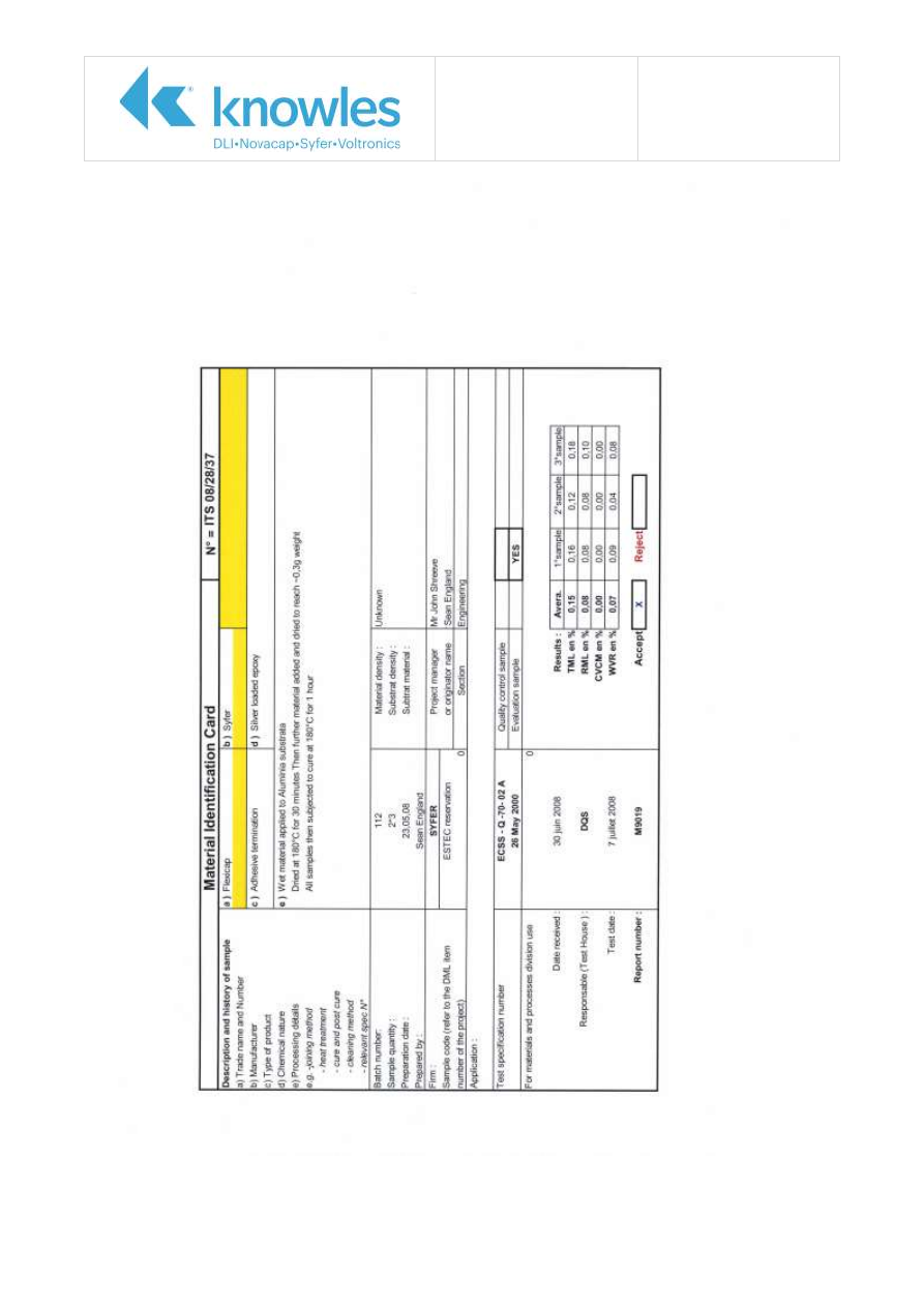
Application Note
Reference No: AN0026
FlexiCap™ Thermal Out-
gassing Test Issue 4
Page 12 of 16
Application Note
Reference No: AN0026
FlexiCap™ Thermal Out-
gassing Test Issue 4
Page 13 of 16
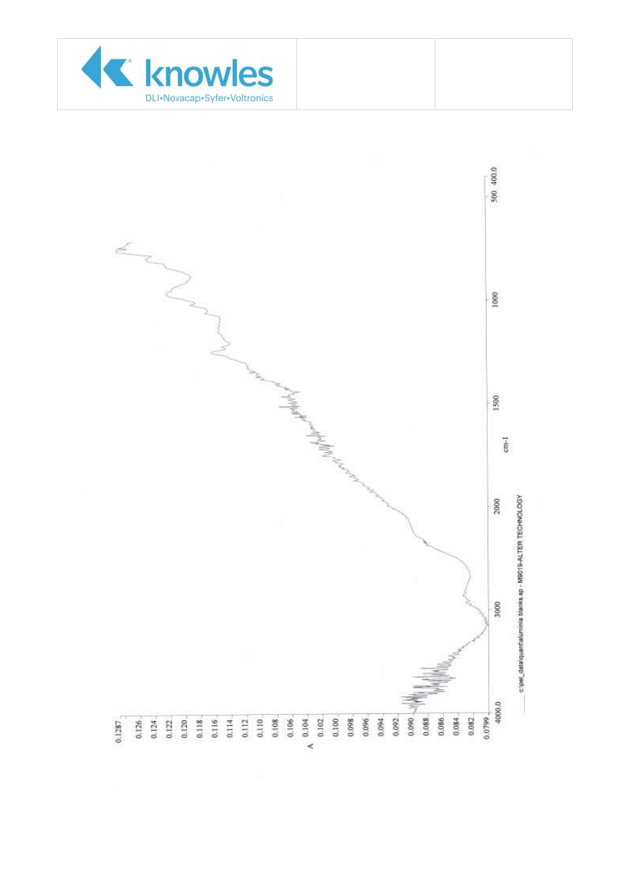
Application Note
Reference No: AN0026
FlexiCap™ Thermal Out-
gassing Test Issue 4
Page 14 of 16
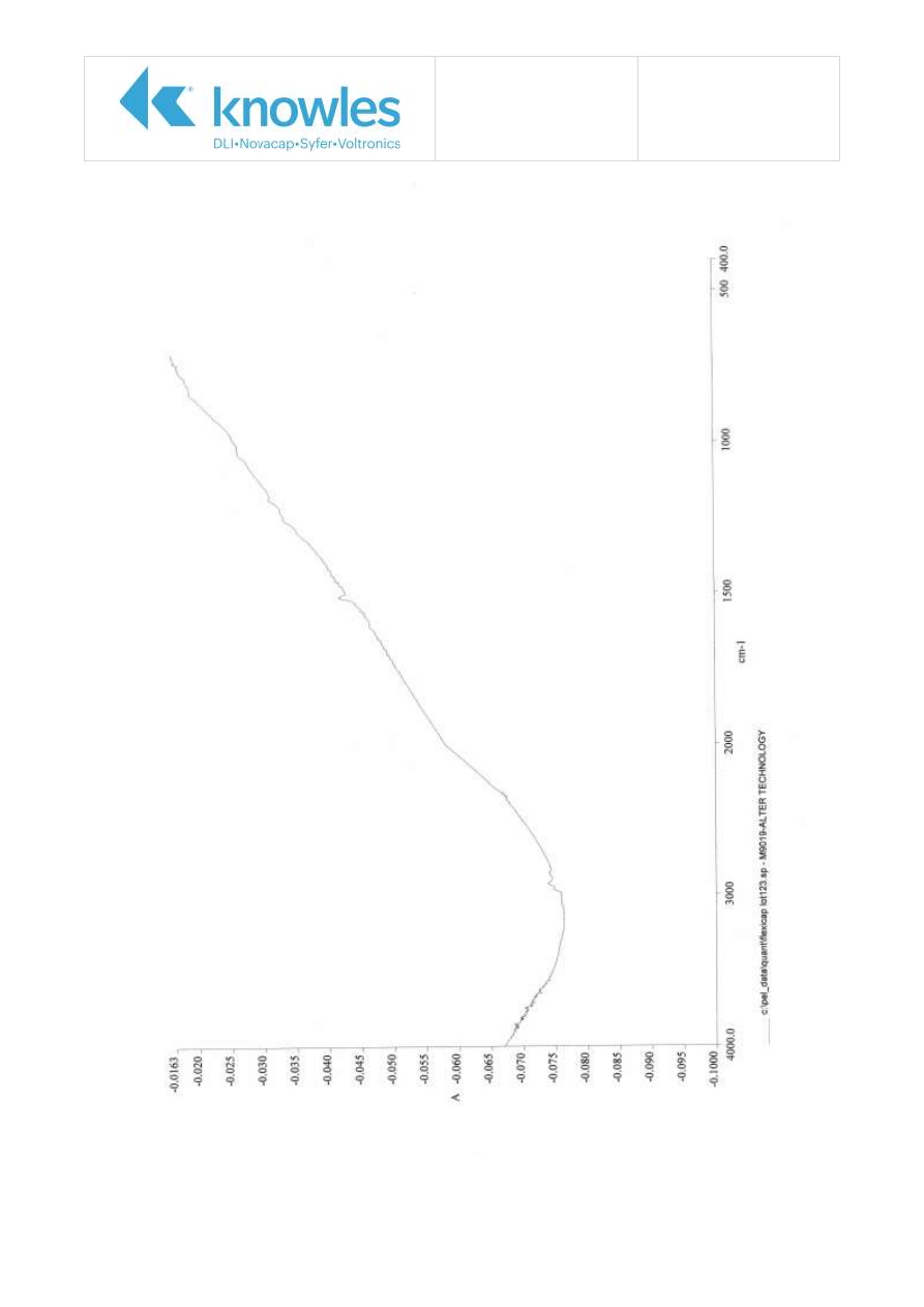
Application Note
Reference No: AN0026
FlexiCap™ Thermal Out-
gassing Test Issue 4
Page 15 of 16
Application Note
Reference No: AN0026
FlexiCap™ Thermal Out-
gassing Test Issue 4
Page 16 of 16

AN0027 Issue 5 - European REACH Regulation
CN# P109825
European REACH Regulation
Registration, Evaluation,
Authorisation and Restriction of
Chemicals
REACH Summary .....................................................................................2
Frequently Asked Questions .......................................................................4
Knowles (UK) Limited,
Old Stoke Road, Arminghall, Norwich,
Norfolk, NR14 8SQ, United Kingdom
Tel: +44 (0) 1603 723300
Tel. (Sales): 01603 723310
Fax: +44 (0) 1603 723301
www.knowlescapacitors.com/syfer

Application Note
Reference No: AN0027
European REACH
Regulation Issue 5
Page 2 of 4
Introduction
The purpose of this application note is to provide a formal response to the many different customer
requests for information on REACH with respect to Syfer Technology Ltd.
This application note provides:
A brief summary of REACH regulation.
How REACH is being addressed by Syfer.
Frequently Asked Questions.
This application note is not intended as a guide to REACH. REACH is a complex regulation that has
different impacts on different organisations depending on the location of the organisation and product
being produced.
The central coordination and implementation role for REACH is being conducted by the European
Chemicals Agency (ECHA) based in Helsinki, Finland. For further information on REACH regulation,
guidance documents and a glossary of terms used refer to the ECHA at
REACH Summary
REACH (
R
egistration,
E
valuation,
A
uthorisation and Restriction of
Ch
emicals) is a European Union
regulation that requires compulsory registration of substances manufactured or imported into the EU in
quantities of 1 tonne or more per year. The regulation applies to substances on their own, in
preparations or in articles (providing certain article threshold limits apply).
The main purpose of REACH is:
To provide a high level of protection of human health and the environment from the use of
chemicals.
To ensure that organisations placing chemicals onto the market (manufactures and importers)
understand and manage the risks associated with the use of the chemical
To allow the free movement of substances on the EU market.
To enhance innovation in and the competitiveness of the EU chemicals industry.
Registration is required if:
Substance quantity > 1 tonne per year either manufactured or imported (note that tonnage
thresholds are per manufacturer or importer not per preparation).
Articles:
o
If the substance is intended to be released and in quantities > 1 tonne per year.
o
If the substance is not intended to be released, but it is classified as a Substance of Very
High Concern (SVHC) such as CMR (Carcinogenic, Mutagenic or Toxic to Reproduction) then
if >1 tonne per year and concentration is >0.1% (w/w).
If a substance is not registered under REACH, it cannot be manufactured, imported or supplied to the
EU market at or above 1 tonne per year unless exemptions apply.
Exemptions are listed in REACH annex IV and annex V such as radioactive substances, waste, recycled
substances (providing same substance as previously registered) food, substances used in the interests
of defence, medicinal products, low risk substances such as oxygen and water, naturally occurring
substances such as minerals and ores – providing that they are not chemically modified.

Application Note
Reference No: AN0027
European REACH
Regulation Issue 5
Page 3 of 4
Key REACH Dates
1 June 2007: REACH came into force.
1 June 2008: European Chemicals Agency becomes operational.
1 June 2008 to 30 November 2008: Pre-registration period.
1 December 2008: Registration for existing substances (that have not been pre-registered)
starts.
1 January 2009: List of pre-registered substances published and SIEFs (Substance Information
Exchange Forum) formed
1 June 2009: First recommendation of priority substances to be considered for authorisation
published by ECHA.
1 December 2010
PHASE 1.
By this date the following pre-registered ‘phase-in’ substances
should have been registered when supplied at:
≥ 1000 tonnes per annum or;
≥ 100 tonnes per annum and classified under CHIP (Chemical Hazard Information and
Packaging for Supply regulations) as very toxic to aquatic organisms or;
≥ 1 tonne per annum and classified under CHIP as Cat 1 or 2 carcinogens, mutagens or
reproductive toxicants
1 June 2013
PHASE 2.
Deadline for registration of substances supplied at ≥ 100 tonnes per
annum.
1 June 2018
PHASE 3.
Deadline for registration of substances supplied at ≥ 1 tonnes per
annum.
Syfer REACH Activities
Syfer maintains both ISO14001 (Environmental Management System) and OHSAS 18001 (Health &
Safety Management System) approvals. Part of the criteria to be approved to these management
systems includes formal processes to ensure that Syfer is compliant with existing relevant legislation
and that Syfer evaluates and implements corresponding actions with respect to new relevant
legislation.
REACH is one of the regulations that is relevant to Syfer and actions/ processes have been
implemented to:
Evaluate the supply chain to ensure that that there is no risk to the continued supply of product
to Syfer and to Syfer’s customers. Where products/ substances are within REACH registration
threshold criteria then confirmation has been obtained from suppliers that registration
requirements will be met.
Review new Safety Data Sheets issued by suppliers to confirm that Syfer exposure scenarios
have been included. If not included then corresponding action will be taken.
Evaluate REACH requirements with respect to any new supplier and/ or new products.
Periodically monitor Syfer substance usage to identify potential registration requirements for
substances currently not requiring registration. For example, if a substance currently used < 1
tonne is started to be used >1 tonne.
Monitor changes to REACH legislation such as updates to the candidate list of SVHC (Substance
of Very High Concern) and implement actions where required.
Application Note
Reference No: AN0027
European REACH
Regulation Issue 5
Page 4 of 4
Frequently Asked Questions
The purpose of this section is to provide answers to the frequently asked questions submitted by
customers regarding Syfer and REACH requirements.
Frequently Asked Questions
Syfer Response
Where is the Syfer manufacturing facility?
Syfer’s factory is located in the United
Kingdom within the EU.
Is Syfer aware of REACH requirements?
Yes
How is Syfer classified with respect to REACH?
Syfer is a downstream user producing/
supplying articles
Has Syfer evaluated REACH implications with
respect to suppliers?
Yes
Has Syfer contacted suppliers to confirm
registration requirements?
Yes
Will there be any disruption of supply from Syfer to
customers?
No
Will there be any products manufactured by Syfer
which will be withdrawn as a result of REACH?
No
Are substances (SVHC) within components
(articles) supplied by Syfer listed on the Candidate
List?
No
Will Syfer monitor changes to REACH such as
Candidate List updates and implement actions?
Yes
Do articles supplied by Syfer contain substances
intended to be released in quantities > 1 tonne per
year.
No

AN0028 Issue 4 – Soldering & Mounting
CN# P109825
Soldering / Mounting Chip
Capacitors, Radial Leaded Capacitors
and EMI Filters
Pad Design for SM Chips and Filters ............................................................2
Reflow Soldering Chip Capacitors and SM Filters ..........................................3
Wave Soldering Chip and Radial Leaded Capacitors ......................................5
Rework of Chip Capacitors .........................................................................6
Hand Soldering Radial Leaded Capacitors ....................................................6
Use of Silver Loaded Epoxy Adhesives ........................................................6
Mounting and Soldering to Panel Mount filters ..............................................7
Mounting into bulkhead .........................................................................7
Terminal Connections ............................................................................7
Knowles (UK) Limited,
Old Stoke Road, Arminghall, Norwich,
Norfolk, NR14 8SQ, United Kingdom
Tel: +44 (0) 1603 723300
Tel. (Sales): 01603 723310
Fax: +44 (0) 1603 723301
www.knowlescapacitors.com/syfer

Application Note
Reference No: AN0028
Soldering & Mounting
Issue 4
Page 2 of 8
Introduction
This application note is intended to give guidance to engineers and board designers on mounting and
soldering Syfer products.
We are increasingly asked to supply definitive soldering information such as solder profiles for specific
applications and board designs. Whilst we will always offer what advice and assistance we can, we are
not able to offer such precise information as it necessitates a thorough knowledge of the entire board
design, other components, materials and equipment being used.
The information we can supply is to indicate general limits and recommendations for successful use of
our products.
Pad Design for SM Chips and Filters
Final pad layout is the responsibility of the board designer and must take into account such factors as
placement accuracy. For this reason any pad dimensions supplied are recommendations and may be
changed by the board designer to suit individual applications.
Syfer conventional 2-terminal chip capacitors can generally be mounted using pad designs in
accordance with IPC-7351, Generic Requirements for Surface Mount Design and Land Pattern
Standards
.
This standard gives recommended land pattern (pad) dimension calculations, but there are some other
factors that can also be considered.
1.
It has been shown that a pad design narrower than the width of the chip capacitor can increase
the mechanical strength of the capacitor joint, leading to an reduction in the incidence of
mechanical cracking of the capacitor due to board distortion. This is achieved at the expense of
a side fillet to the solder joint. Syfer do not consider this a problem, but the use of this design is
left to the discretion of the board manufacturer.
2.
The position of the chip on the board should be considered to reduce the chances of mechanical
cracking occurring as a result of board bending. Generally, the chip should be mounted parallel
to any potential bend line. 3-Terminal and larger components are more susceptible to
mechanical cracking. Refer to Syfer application note AN0005 for more information on
mechanical cracking and AN0001 for details of Syfer Flexicap polymer termination.
3.
Where high voltages are involved, particularly with smaller size components, it can be
advantageous to machine a slot in the board between the pads allowing access to the underside
of the component. This ensures adequate removal of debris (eg flux / solder balls) from under
the component after soldering and cleaning, and allows complete coverage with conformal
coating to prevent electrical flashover.
3-Terminal components (EMI filter chips, SM filters etc) are not specifically covered by IPC-7351,
but recommended pad dimensions are included in the Syfer catalogue / website for these
components.
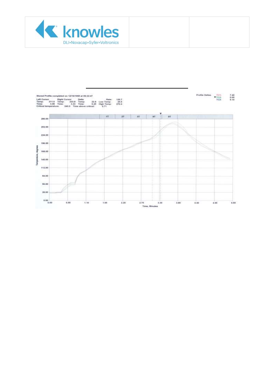
Application Note
Reference No: AN0028
Soldering & Mounting
Issue 4
Page 3 of 8
Reflow Soldering Chip Capacitors and SM Filters
Syfer recommend a reflow profile of the same general shape as shown below for soldering SM
capacitors. This is as generally defined in IPC / JEDEC J-STD-020D.
Recommended Reflow Soldering Profile
When discussing a reflow profile, we can only give a general recommendation as to the shape of the
profile. We cannot give a definitive profile of the actual peak temperatures, as this is dependant on a
number of factors which can only be decided by the assembler – the type of solder used, the size,
specification and arrangement of other components on the board and the overall thermal mass of the
board.
All Syfer Sn/Ni plated termination chip capacitors are compatible with both conventional and lead free
soldering, with peak temperatures of 260ºC to 270ºC acceptable. Any solder types with liquidus
temperatures suitably low can be used.
SM Filters type SBSP can be treated as conventional chip capacitors as above, but types SBSG and
SBSM have a soldered construction and must not be allowed to exceed 220ºC – above this
temperature damage will occur.
Generally, we recommend that the ramp is maintained such that the components see a temperature
rise of 1.5ºC to 4ºC per second. This is to maintain temperature uniformity through the MLCC and
prevent the formation of thermal gradients within the ceramic. In practise, thermal gradients larger
than this can still be acceptable, and smaller chip sizes are less susceptible to problems.
In house, Syfer tend to ramp direct to reflow, without a specific dwell or temperature soak. A
temperature soak is perfectly acceptable if board complexity or other components demand it or the
assemblers own preference is to do so.
The time for which the solder is molten should be maintained at a minimum, so as to prevent solder
leaching, although this is less of a problem with Sn/Ni plated terminations. Extended times above
230ºC can cause problems with oxidisation of Sn plating. Use of inert atmosphere can help if this

Application Note
Reference No: AN0028
Soldering & Mounting
Issue 4
Page 4 of 8
problem is encountered. PdAg terminations can be particularly susceptible to leaching with lead free,
tin rich solders and trials are recommended for this combination.
To allow multiple reflow operations, Syfer Sn/Ni plated termination chip capacitors can withstand up to
3 reflow operations at temperatures up to 260ºC.
Cooling to ambient temperature should be allowed to occur naturally, particularly if larger chip sizes
are being soldered. Natural cooling allows a gradual relaxation of thermal mismatch stresses in the
solder joints, very important for large chips. Draughts should be avoided. Forced air cooling can induce
thermal breakage, and cleaning with cold fluids immediately after a soldering process may result in
cracked MLC capacitors.
Generally, Syfer recommend convection reflow (also referred to as hot air reflow) as the best method
of soldering chip capacitors.
IR reflow is acceptable, but care must be taken when recording and setting soldering profiles as the
heating effect is related to the heat absorption rate and thermal conductivity of the materials used –
for example the solder paste, ceramic body, metal plating and board material will all absorb heat at
slightly different rates. In extreme cases this can induce large temperature deltas in the capacitors.
Finally, IR reflow can be susceptible to shadowing (some components blocking direct heat transfer to
others) and board layout must be considered accordingly.
Vapour phase reflow soldering can be used, but the nature of this method of applying heat is such that
very high temperature ramp rates can be observed. Particularly with larger capacitors, this has been
shown to induce micro cracks due to induced temperature deltas. Pre-heat of the components must be
carefully controlled.
Radial leaded capacitors can be soldered using pin intrusive reflow techniques, but only if the
maximum temperature is restricted to 220ºC as these components are soldered construction as SM
filters.
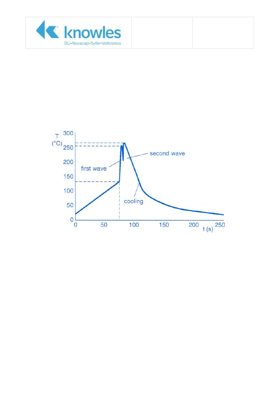
Application Note
Reference No: AN0028
Soldering & Mounting
Issue 4
Page 5 of 8
Wave Soldering Chip and Radial Leaded Capacitors
Wave soldering is generally acceptable, but the thermal stresses in the wave can lead to potential
problems with larger or thicker chips. Particular care should be taken when soldering SM chips larger
than size 1210 and with a thickness greater than 1.0mm for this reason. Any chip capacitor should be
verified as compatible with a particular wave solder profile.
NOTE – all temperatures refer to wave side of the board. Radial capacitors can be wave
soldered into through holes, but the encapsulated capacitor body must always be on the top
of the board and must never be immersed in the wave.
If wave soldering is to be carried out, we recommend a profile of the general shape as below (single
wave of the same general shape is also acceptable).
Maximum permissible wave temperature is 270ºC for SM chips and 260ºC for Radial Leaded capacitors
– see also note above regarding radial leaded capacitors.
The total immersion time in the solder should be kept to a minimum. It is strongly recommended that
Sn/Ni plated terminations are specified for wave soldering applications. PdAg termination is particularly
susceptible to leaching when subjected to lead free wave soldering and care should be taken if it is
used for this application.
Total immersion exposure time for Sn/Ni terminations is 30s at a wave temperature of 260ºC. Note
that for multiple soldering operations, including the rework, the soldering time is cumulative.
The pre-heat ramp should be such that the components see a temperature rise of 1.5ºC to 4ºC per
second as for reflow soldering. This is to maintain temperature uniformity through the MLCC and
prevent the formation of thermal gradients within the ceramic.
The preheat temperature should be within 120ºC maximum (100ºC preferred) of the maximum solder
temperature to minimise thermal shock.
Design and jigging should be sufficient to prevent board warping during the soldering process. Board
warping can introduce stresses that result in problems such as mechanical cracking which may only be
apparent at a later stage.
Cooling to ambient temperature should be allowed to occur naturally if possible, particularly if larger
chip sizes are being soldered. Natural cooling allows a gradual relaxation of thermal mismatch stresses

Application Note
Reference No: AN0028
Soldering & Mounting
Issue 4
Page 6 of 8
in the solder joints, very important for large chips. Draughts should be avoided. Forced air cooling can
induce thermal breakage, and cleaning with cold fluids immediately after a soldering process may
result in cracked MLC capacitors.
Rework of Chip Capacitors
If it is necessary to remove and replace a chip capacitor (rework), then particular care must be taken
to prevent thermal gradients being generated within the ceramic body. Thermal gradients can result in
micro cracks being generated, which can result in subsequent failure.
Syfer recommend hot air/ gas as the preferred method for applying heat for rework. Apply even heat
surrounding the component to minimise internal thermal gradients.
Syfer do not recommend the use of soldering irons or other techniques that apply direct heat to the
chip or surrounding area, as these can cause severe thermal mismatch gradients within the
components resulting in micro cracks being generated. If soldering irons must be used it is important
not to allow the iron tip to come into direct contact with the chip capacitor, but is applied to the pad
adjacent to the capacitor and the heat allowed to soak gradually into the chip.
Minimise the rework heat duration, and allow components to cool naturally after soldering. Do not force
cool as this can induce cracking. Ensure components are at room temperature before any cleaning
process.
Hand Soldering Radial Leaded Capacitors
Radial capacitors can be hand soldered into boards using soldering irons, provided care is taken not to
touch the body of the capacitor with the iron tip. Soldering should be carried out from the opposite side
of the board to the radial to minimise the risk of damage to the capacitor body.
Generally, the tip temperature of the iron should not exceed 300°C and the dwell time should be 3-5
seconds maximum to minimise the risk of cracking the capacitor due to thermal shock. Where possible,
a heat sink should be used between the solder joint and the body, especially if longer dwell times are
required.
Use of Silver Loaded Epoxy Adhesives
Chip capacitors can be mounted to circuit boards using silver loaded adhesive provided the termination
material of the capacitor is selected to be compatible with the silver loaded adhesive. This is normally
PdAg. Standard tin finishes are often not recommended for use with silver loaded epoxies as there can
be electrical and mechanical issues with the joint integrity due to material mismatch.

Application Note
Reference No: AN0028
Soldering & Mounting
Issue 4
Page 7 of 8
Mounting and Soldering to Panel Mount filters
The ceramic capacitor, which is the heart of the filter, can be damaged by thermal and mechanical
shock, as well as by over-voltage. Care should be taken to minimise the risk of stress when mounting
the filter to a panel and when soldering wire to the filter terminations.
It is important to mount the filter to the bulkhead or panel using the recommended mounting torque,
otherwise damage may be caused to the capacitor due to distortion of the case. When a threaded hole
is to be utilised, the maximum mounting torque should be 50% of the specified figure which relates to
unthreaded holes. For details of torque figures for each filter range, please see below.
Mounting into bulkhead
Thread
Torque (max)
With nut
Into tapped hole
M2.5 & 4-40UNC
-
0.15Nm (1.3 lbf in)
M3
0.25Nm (2.2 lbf in)
0.15Nm (1.3 lbf in)
6-32 UNC
0.3Nm (2.7 lbf in)
0.15Nm (1.3 lbf in)
M3.5
0.35Nm (3.1 lbf in)
0.18Nm (1.6 lbf in)
M4 & 8-32 UNC
0.5Nm (4.4 lbf in)
0.25Nm (2.2 lbf in)
M5, 12-32 UNEF & 2BA
0.6Nm (5.3 lbf in)
0.3Nm (2.7 lbf in)
M6 & ¼-28 UNF
0.9Nm (8.0 lbf in)
-
M8
1.0Nm (8.9 lbf in)
0.5Nm (4.4 lbf in)
M10
3Nm (26.6 lbf in)
-
M12
4Nm (35.4 lbf in)
-
M16
7Nm (61.7 lbf in)
-
M20
10Nm (88.5 lbf in)
-
M24, M25
14Nm (123.9 lbf in)
-
Terminal Connections
Thread
Torque (max)
M3
0.5Nm (4.4 lbf in)
M4
1.2Nm (10.6 lbf in)
M6
2.5Nm (22.1 lbf in)
M8
5.0Nm (44.3 lbf in)
When tightening terminal connections, always use 2 spanners to prevent twisting of terminal.
For threads not listed, please contact the factory for recommended tightening torque.
Hexagonal devices should be assembled using a suitable socket. Round bodied filters may be fitted to
the panel in one of two ways (and should not be fitted using pliers or other similar tools which may
damage them):

Application Note
Reference No: AN0028
Soldering & Mounting
Issue 4
Page 8 of 8
● Round bodies with slotted tops are designed to be screwed directly into a panel using a simple
purpose-designed tool.
● Round bodies without slotted tops are intended to be inserted into slotted holes and retained
with a nut.
To ensure the proper operation of the filters, the filter body should be adequately grounded to the
panel to allow an effective path for the interference. The use of locking adhesives is not recommended,
but if used should be applied after the filter has been fitted.
Users should be aware that the majority of filters have an undercut between the thread and the
mounting flange of the body, equal to 1.5 x the pitch of the thread. Mounting into a panel thinner than
this undercut length may result in problems with thread mating and filter position. It is recommended
that a panel thicker than this undercut length be used wherever possible.
Filters with a thread run-out will have an un-threaded portion between the head and the start of the
thread. This may need to be allowed for in hole design.
Maximum plate thickness is specified for each filter in order that the nut can be fully engaged even
when using a washer.
When Soldering to axial wire leads, the tip temperature of the iron should not exceed 300°C and the
dwell time should be 3-5 seconds maximum to minimise the risk of cracking the capacitor due to
thermal shock.
Where possible, a heat sink should be used between the solder joint and the body, especially if longer
dwell times are required.
Bending or cropping of the filter terminations should not be carried out within 4mm (0.157”) of the
epoxy encapsulation and the wire should be supported when cropping wherever possible.

AN0029 Issue 3 – Use of Syfer MLCCs at High Temperatures
P109825
Use of Syfer Multilayer Ceramic
Capacitors at Higher Temperatures
Syfer Multilayer Ceramic Capacitors are approved for use over the temperature range -55
o
C to +125
o
C
(150
o
C for X8R).
This application note provides information on how Syfer product could be suitable for
use at elevated temperatures of up to 200
o
C.
Basic Electrical Properties at High Temperatures ..........................................4
Knowles (UK) Limited,
Old Stoke Road, Arminghall, Norwich,
Norfolk, NR14 8SQ, United Kingdom
Tel: +44 (0) 1603 723300
Tel. (Sales): 01603 723310
Fax: +44 (0) 1603 723301
www.knowlescapacitors.com/syfer
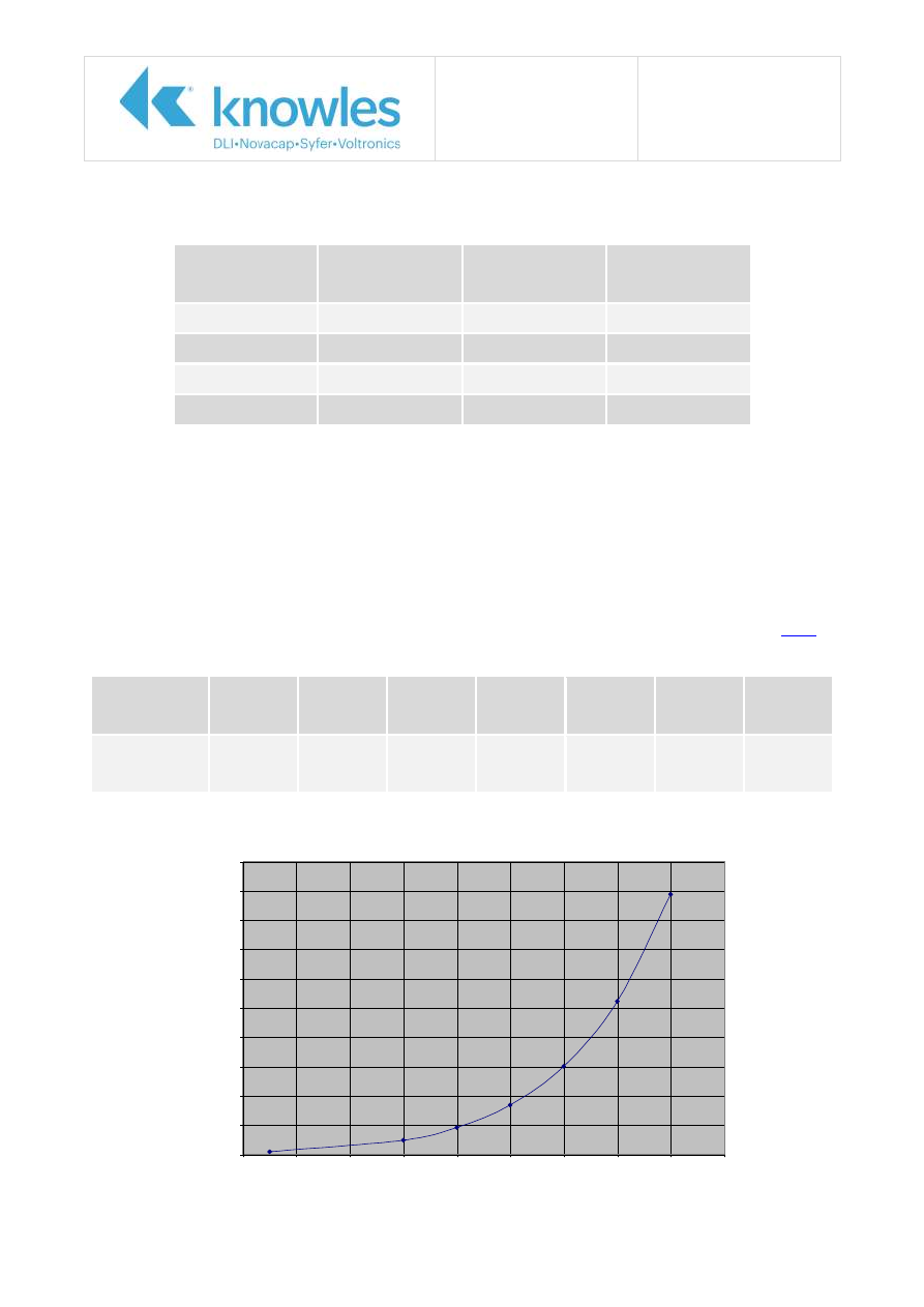
Application Note
Reference No: AN0029
MLCCs at High
Temperatures Issue 3
Page 2 of 7
Introduction
Syfer products are rated over the temperature range of -55
o
C to +150
o
C as shown below:
Dielectric
Classification
Lower
Temperature
Upper
Temperature
Maximum Cap
Change
C0G
-55˚C
+125˚C
±30ppm/
o
C
X5R
-55˚C
+85˚C
±15%
X7R
-55˚C
+125˚C
±15%
X8R
-55˚C
+150˚C
±15%
For certain automotive and industrial applications a wider temperature range is often requested,
particularly for temperatures up to 200
o
C. Standard product may not be suitable for use above the
upper rated temperature of 125
o
C, but after extensive testing performed at our manufacturing facility
it is possible for Syfer to make recommendations on part suitability for use at higher temperatures. It
should be noted however, that although parts will function at temperatures up to 200
o
C the electrical
properties will not meet the normal C0G, X5R, X7R or X8R specifications.
Background
The reliability of multilayer ceramic capacitors is directly related to the voltage applied and the
operating temperature as detailed in Syfer’s AN0004 ‘Quality and Reliability Data’ (
The acceleration factor due to temperature increases very significantly as temperature is increased:
Stress
Temperature
125˚C
150˚C
160˚C
170˚C
180˚C
190˚C
200˚C
Acceleration
Factor
871
4884
9203
16854
30051
52258
88776
Acceleration Factor Vs Stress Temperature
0
10000
20000
30000
40000
50000
60000
70000
80000
90000
100000
120
130
140
150
160
170
180
190
200
210
Temperature oC
A
F
t

Application Note
Reference No: AN0029
MLCCs at High
Temperatures Issue 3
Page 3 of 7
Thermal stress alone is sufficient to cause electrical failure. Thermal breakdown takes place when heat
is generated in the dielectric at a higher rate than it can be conducted away. This leads to increased
conductivity, more heat generation and eventually to instability in the form of an uncontrolled, often
very rapid temperature rise. The temperatures attained when a capacitor discharges through a region
of localised thermal runaway can be high enough to melt the dielectric material.
When determining whether a particular component is suitable for use at high temperatures, customers
must consider the thermal stress, and the effect of the elevated temperature on basic electrical
properties such as capacitance, dissipation factor and insulation resistance.
Component Testing
Syfer has undertaken extensive testing of standard components made from each dielectric material
type used in the manufacture of multilayer chip capacitors. The basic electrical properties of Syfer
components at high temperatures are exhibited graphically in the next section of this document.
Reliability testing of components at temperatures of up to 200
o
C has also been carried out.
Recommendations for high temperature applications based on these results can be found in the final
section of this document.
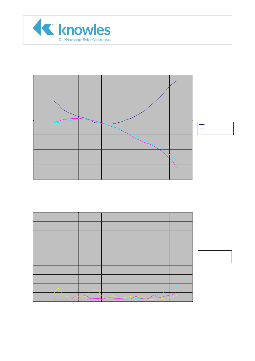
Application Note
Reference No: AN0029
MLCCs at High
Temperatures Issue 3
Page 4 of 7
Basic Electrical Properties at High Temperatures
C0G Temperature Characteristic - Capacitance
-80
-60
-40
-20
0
20
40
60
-100
-50
0
50
100
150
200
250
Temperature oC
C
a
p
c
h
a
n
g
e
(p
a
rts
p
e
r
m
ill
io
n
/o
C
)
Low K material
High K material
High voltage material
C0G Temperature Characteristic - Dissipation Factor
0
0.0005
0.001
0.0015
0.002
0.0025
0.003
0.0035
0.004
0.0045
0.005
-100
-50
0
50
100
150
200
250
Temperature oC
D
is
s
ipa
ti
on
Fa
c
tor
High voltage material
High K material
Low K material
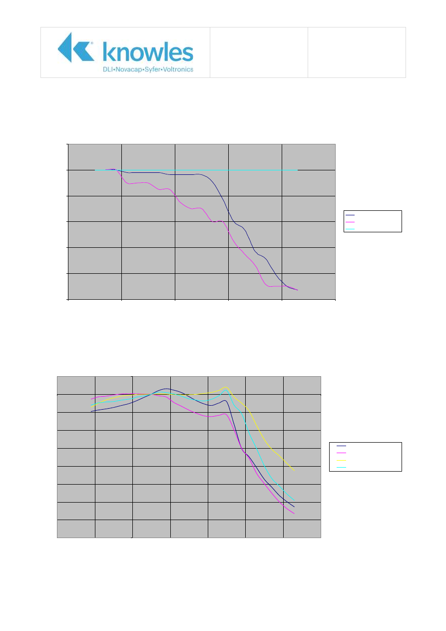
Application Note
Reference No: AN0029
MLCCs at High
Temperatures Issue 3
Page 5 of 7
C0G Temperature Characteristic - Insulation Resistance
0
20
40
60
80
100
120
0
50
100
150
200
250
Temperature oC
IR
c
ha
ng
e
(
%
of
r
oo
m
t
e
m
pe
ra
ture
v
a
lue
)
High voltage material
High K material
Low K material
X5R / X7R / X8R Temperature Characteristic - Capacitance
-80
-70
-60
-50
-40
-30
-20
-10
0
10
-100
-50
0
50
100
150
200
250
Temperature oC
Capacitan
ce
chang
e (%
)
High voltage material
High K material
X8R material
Mid K material
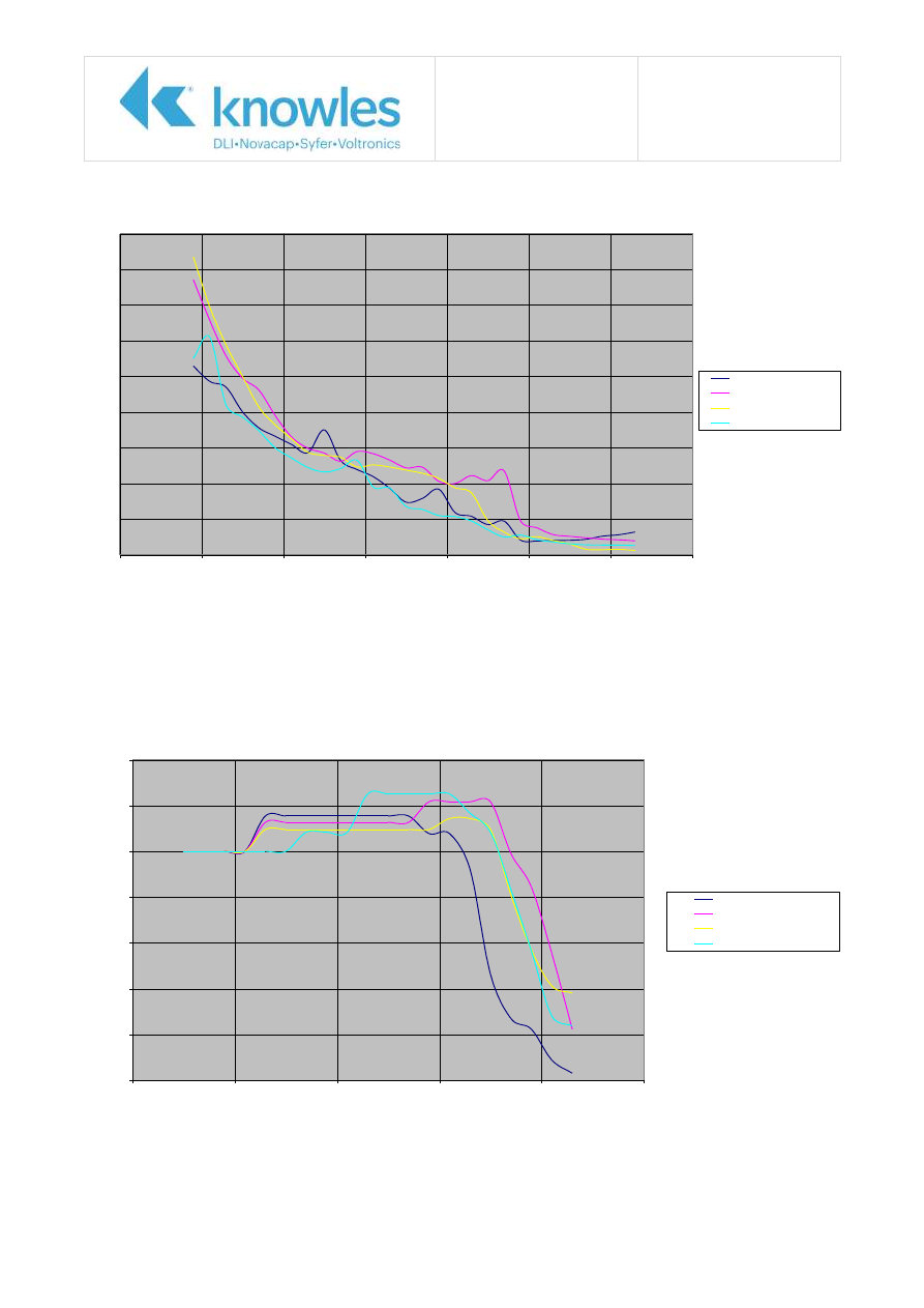
Application Note
Reference No: AN0029
MLCCs at High
Temperatures Issue 3
Page 6 of 7
X5R / X7R / X8R Temperature Characteristic - Dissipation Factor
0
0.005
0.01
0.015
0.02
0.025
0.03
0.035
0.04
0.045
-100
-50
0
50
100
150
200
250
Temperature oC
Diss
ipat
ion
Fact
o
r
High voltage material
High K material
X8R material
Mid K material
X5R / X7R / X8R Temperature Characteristic - Insulation Resistance
0
20
40
60
80
100
120
140
0
50
100
150
200
250
Temperature oC
IR chang
e (%
of
r
o
o
m t
emp
er
atu
re v
alue)
High K material
Mid K material
High voltage material
X8R material
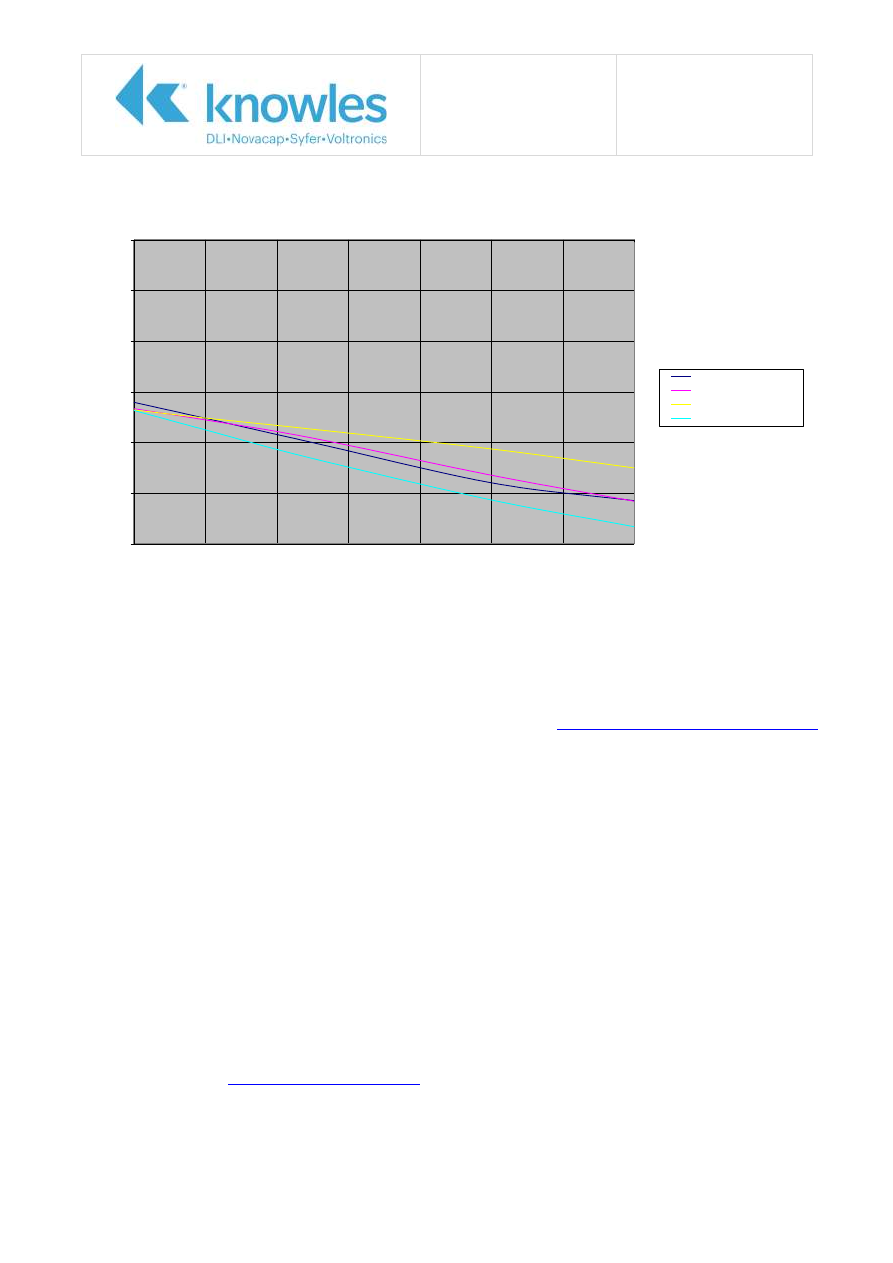
Application Note
Reference No: AN0029
MLCCs at High
Temperatures Issue 3
Page 7 of 7
X5R / X7R / X8R Temperature Characteristic - Voltage Coefficient
-60
-50
-40
-30
-20
-10
0
150
160
170
180
190
200
210
220
Temperature oC
T
ypical
Cap Ch
ang
e wit
h
app
lie
d
volt
age
High voltage material
High K material
X8R material
Mid K material
Recommendations
As component reliability is detrimentally affected due to thermal stresses it is not recommended that
standard components are used at temperatures >125˚C however:
A - For temperatures up to 160˚C
, most standard components will give reliable performance, but
the Syfer recommendation is for the component user to select components with a voltage rating ≥30%
higher than the component that would normally be selected.
www.knowlescapacitors.com/syfer
Quick reference guides for max cap per size/ voltage for standard product)
For example, if a 0805 50V 10nF component would normally be used, the recommendation
would be to use an 0805 100V 10nF part – NB the 0805 63V 10nF would not meet the
recommendation as the voltage increase is only 26%.
B - For temperatures >160˚C
, Syfer test data shows that the reliability is affected exponentially
in a similar way to that shown on the thermal stress graph above. This makes it very difficult
to provide a simple set of rules for component users to apply for use between >160
o
C and
200
o
C.
Consequently, for component use >160˚C, Syfer recommends the user contacts our technical
team with details of the exact application and Syfer will recommend the most suitable
component. This will ensure that the customer will always get the most reliable and cost
effective solution to their needs.
As an example, the recommended component size for a particular application may be a 1206
size chip for use at 170˚C, but for the same capacitance value and working voltage an 1812
chip may be needed for use at 200˚C.
For further information or technical assistance please contact our Sales Department on +44 1603
723310 or by Email at

AN0031 Issue 3 - Varistor Planar Arrays
P109825
Metal Oxide Varistor Planar Arrays
How can MOV Planars be utilised? ..............................................................4
Types of transient and capabilities ..............................................................5
Advantages over other technologies ...........................................................5
Knowles (UK) Limited,
Old Stoke Road, Arminghall, Norwich,
Norfolk, NR14 8SQ, United Kingdom
Tel: +44 (0) 1603 723300
Tel. (Sales): 01603 723310
Fax: +44 (0) 1603 723301
www.knowlescapacitors.com/syfer
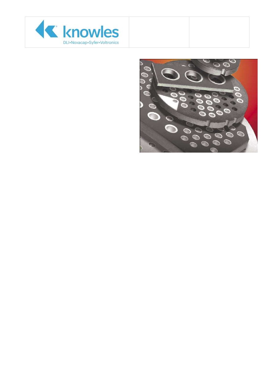
Application Note
Reference No: AN0031
Varistor Planar Arrays
Issue 3
Page 2 of 7
Introduction
Syfer Technology Limited has been manufacturing
and supplying Planar Capacitor Arrays since 1990,
and is the world's leading supplier. The multilayer
ceramic Planar Capacitor Array is an application
specific component designed for use in multi-line
EMI/RFI filter circuits, typically found in filtered
connectors. Planar Capacitor Array technology
affords the user weight and volumetric efficiency
as well as performance and reliability advantages
compared to other capacitor technologies. Syfer's
leading position has been achieved through
utilisation of the advantages inherent in our "Wet-
Stack" process. A stress-free component is
produced with mechanical precision, enabling a
filter assembly to withstand the most rigorous of
electrical specifications.
The MOV (Metal Oxide Varistor) Planar Array is an extension of the Capacitor Planar Array concept also
for use in filtered connectors. MOV Planar Arrays, when used in isolation or together with Syfer’s
Capacitor Planar Arrays, can provide a complete over-voltage transient protection and EMI filtering
solution to connector manufacturers. With the MOV Planar Array’s inherent capacitance, it can be used
as a simple C filter or as one half of a Pi or unbalanced Pi filters. The same volumetric benefits apply to
MOV planars as to capacitor planars, the space weight and packaging savings can be significant.
What is an MOV?
MOV stands for Metal Oxide Varistor. MOVs are over voltage transient protection devices which are
available in many formats, historically they were high voltage single layer radial leaded components
but are now most commonly seen in surface mount form utilising multilayer construction as found in
the MLCC industry. Syfer have taken the technology one step further and produce multilayer MOVs in
planar array and discoidal formats.
Metal oxide varistor devices consist mainly of zinc oxide, this base material is then doped with small
quantities of bismuth, cobalt and manganese amongst other metal oxide additives. The varistor is built
up from layers of the zinc oxide material interleaved with platinum forming the highly conductive
electrodes, during the firing process the dopants within the dielectric material migrate to the grain
boundaries and cause each grain to act as a P-N junction with an activation voltage of approximately
3.6 volts. In order to achieve higher working voltages many layers of ceramic are used, the grains are
effectively linked in series and parallel creating multiples of their discrete properties.
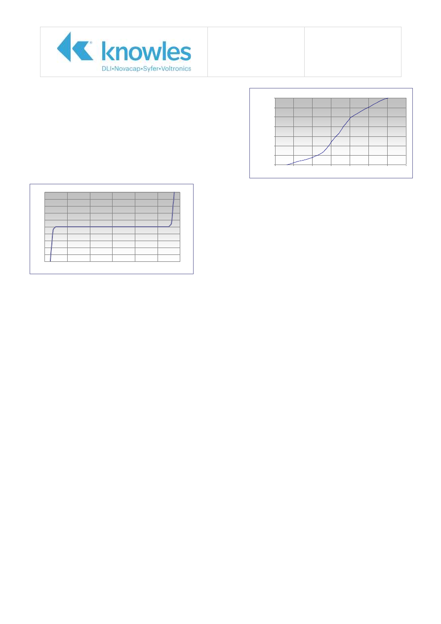
Application Note
Reference No: AN0031
Varistor Planar Arrays
Issue 3
Page 3 of 7
At operational, or “Working”, voltages an MOV acts as a
high value resistor which obeys Ohms law with a
maximum leakage current specified of 5μA, once the
voltage reaches a certain value the device becomes
highly conductive and provides a path to ground, it is
this property which makes it ideal for use as transient
protection. Other points on the V-I curve are specified at
1mA of current flow at “Nominal” or “Breakdown”
voltage, and 5 or 10A of current at “Clamp Voltage”.
These properties are bi-directional so the MOV will
perform equally as well for both positive and negative
transient events, Fig.2. Figure 1 shows an example of
the V-I properties of a 47V working component, note
the log scale on the Y axis, at 47V current is approx
5μA, Nominal voltage at 1mA is 63V, Clamp Voltage at
10A is 90V. In this case the part specification would be:
Working Voltage 47V, Nominal Voltage 53 – 69V and
Clamp Voltage 100V maximum at 10A.
When exposed to high transient voltage, the varistor clamps the voltage to a safe level. A metal oxide
varistor absorbs potentially destructive energy and dissipates it as heat, thus protecting vulnerable
circuit components and preventing system damage. There are limitations to the level of current which
can flow and the amount of energy which can dissipate within the varistor; typical limits are 500A peak
current and 3J of energy with a transient. These limitations are dependant on the geometry of the
planar, high density and thin varieties may have lower capabilities.
Example - 47V Working
0.000001
0.00001
0.0001
0.001
0.01
0.1
1
10
30
40
50
60
70
80
90
100
Voltage/V
C
u
rr
e
n
t/
A
Varistor V-I curve
0
Voltage/V
C
u
rr
e
n
t/
A
0
Fig. 1 Current vs. Voltage 47V working
Fig. 2 Bi directional properties
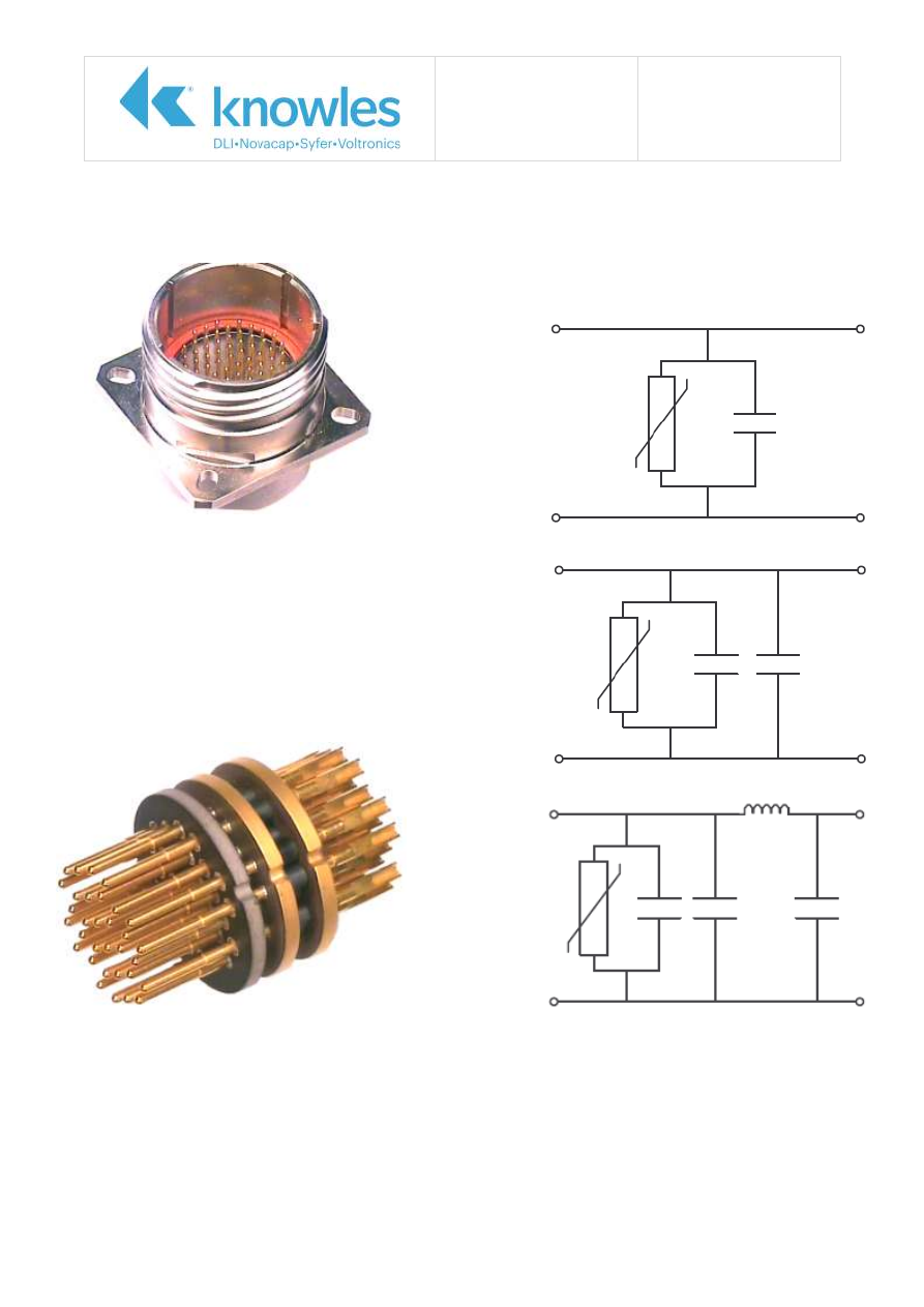
Application Note
Reference No: AN0031
Varistor Planar Arrays
Issue 3
Page 4 of 7
How can MOV Planars be utilised?
The MOV array is designed for use within the shell of a mil
or aerospace type connector either complimentary to, or
replacing a capacitor planar array.
Common circuit configurations include:
1. A simple low capacitance C filter consisting solely of the
MOV: Fig. 3.
2. A high capacitance C filter when used in parallel with a
capacitor planar: Fig. 4.
3. A balanced or unbalanced Pi filter; additional capacitor
planars can be matched with the varistor planar to provide
equal capacitance either side of the inductor. Fig. 5.
Fig. 6 shows the typical format of an MOV protected connector, the MOV is the left hand planar of the
three, the other two are capacitor planars with ferrite beads placed over the pins in between to form an
unbalanced Pi filter.
Fig. 4 MOV C filter with additional capacitor planar
Fig. 6
The internal configuration of a varistor
protected unbalanced
Pi
Fig. 5 MOV protected Pi filter
Fig. 3 MOV C filter
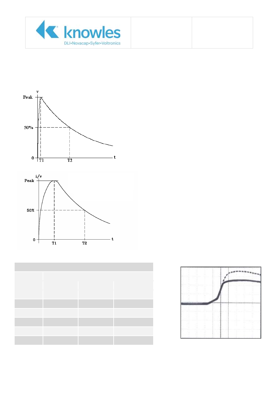
Application Note
Reference No: AN0031
Varistor Planar Arrays
Issue 3
Page 5 of 7
Types of transient and capabilities
MOVs are suitable for protecting against several types of transient event. With a material response
time of less than 500ps and a no lead/track low inductance geometry MOVs are
More than capable of suppressing lightning induced transients.
Syfer MOV arrays have been tested to RTCA
DO160-E section 22 waveform 4 level 5 and
waveform 5 level 3, see Fig. 10. 47V and 8V parts
were tested for leakage current, nominal voltage
and clamp voltage, the same parts were the
subjected to 500 pulses at 10 second intervals and
then re-measured, failure is defined as greater
than a 10% shift in parameters, no failures were
observed.
Testing has also been undertaken in order to
demonstrate the speed of response capabilities.
Parts were subjected to a 1MHz 175V square wave
with a rise time of less than 400ns, Fig. 9 shows
the response of a 47V working planar, note there
is no voltage overshoot present prior to full
clamping.
Test Levels for Pin Injection as per RTCA/DO-160E
Level
Waveforms
3
4
5A
Voc/Isc
Voc/Isc
Voc/Isc
1
100/4
50/10
50/50
2
250/10
125/25
125/125
3
600/24
300/60
300/300
4
1500/60
750/150
750/750
5
3200/128
1600/320
1600/1600
4
T1 = 6.4μs ±20%
T2 = 69 ±20%
Fig. 7 RTCA/DO-160E Waveform 4
5A
T1 = 40μs ±20%
T2 = 120 ±20%
Fig. 8 RTCA/DO-160E Waveform 5A
Fig. 9 Response of 47V Working - no
voltage overshoot present.
Fig. 10 RTCA/DO-160E levels
Application Note
Reference No: AN0031
Varistor Planar Arrays
Issue 3
Page 6 of 7
Advantages over other technologies
The main alternatives to MOV planar arrays are TVS (Transient Voltage
Suppression) diodes. Each technology has its advantages in different
circumstances, Diodes are available for lower working voltages than
Syfer MOV arrays and also have lower leakage and sharper clamping
characteristics. MOVs can compete on Energy and Current capabilities
and are more volumetrically efficient as many components are
contained within one device, this also has cost saving benefits.
The images to the right and below illustrate some of the drawbacks of
TVS diodes, not only are extra piece parts required to mount and
connect the diodes to the pins but those extra parts add significant bulk
and weight to the overall connector package. The planar array can be
manufactured to the same
dimensional specifications and
tolerances as the capacitor planars generally used in the connector;
this means that adding transient suppression need not have an
impact on the size of the connector. See Fig. 6.
No other transient voltage suppression technology can match the
MOV planar when it comes to efficient use of connector real estate.
Syfer has a stock and secure supply of raw materials and
manufacture to demand. With a typical lead-time of 8 weeks
concerns over consistency of supply, which can be a problem for
users of diodes, need not be an issue.
Range
Syfer Capacitor and MOV planar arrays are generally customer specific items, we work with our
customers in order to provide a bespoke product which meets their exact requirements. For the
purposes of providing a guide to the capabilities available in various planforms and hole sizes a range
showing the maximum energy and peak current ratings can be seen below. A mix of up to three
voltages can be combined in one array depending on available space and specification requirements.
Hole size 22
Thickness
Working Voltage
8V
15V
28V
33V
47V
65 thou/mils
1.2J/500A 1.2J/440A 1.1J/240A 1.0J/200A 0.5J/80A
100 thou/mils
1.2J/500A 1.7J/500A 1.8J/440A 1.7J/360A 1.2J/160A
125 thou/mils
1.2J/500A 1.7J/500A 2.4J/500A 2.3J/480A 1.5J/200A

Application Note
Reference No: AN0031
Varistor Planar Arrays
Issue 3
Page 7 of 7
Hole size 20
Thickness
Working Voltage
8V
15V
28V
33V
47V
65 thou/mils
1.3J/500A 1.5J/500A 2.2J/500A 2.5J/500A 2.7J/500A
100 thou/mils
1.3J/500A 1.5J/500A 2.2J/500A 2.5J/500A 3.0J/500A
125 thou/mils
1.3J/500A 1.5J/500A 2.2J/500A 2.5J/500A 3.2J/500A
Hole size 16
Thickness
Working Voltage
8V
15V
28V
33V
47V
65 thou/mils
1.3J/500A 1.5J/500A 2.2J/500A 2.5J/500A 3.2J/500A
100 thou/mils
1.3J/500A 1.5J/500A 2.2J/500A 2.5J/500A 3.2J/500A
125 thou/mils
1.3J/500A 1.5J/500A 2.2J/500A 2.5J/500A 3.2J/500A
Syfer MOV planars are available in a wide range of standard mil sizes, examples:
Circular shell sizes 8 – 24
Arinc 600 and 404 series
Rect 24308 series
Also available are discoidal MOVs from 4.5mm OD upwards.
Other standard and non-standard sizes and specifications may be available; contact Syfer Technology
Ltd at

AN0032 Issue 3 – MLCC for use in Modems
P109825
MLCC for use in Modems
Knowles (UK) Limited,
Old Stoke Road, Arminghall, Norwich,
Norfolk, NR14 8SQ, United Kingdom
Tel: +44 (0) 1603 723300
Tel. (Sales): 01603 723310
Fax: +44 (0) 1603 723301
www.knowlescapacitors.com/syfer
Application Note
Reference No: AN0032
MLCC for use in Modems
Issue 3
Page 2 of 3
Introduction
Syfer Technology Limited is a premier global source for application specific multilayer ceramic
capacitors and EMI suppression filters. Our comprehensive product range includes many application-
specific capacitors, including FlexiCap™, as well as standard voltages and capacitance values. All our
products are available in small, medium and large volumes. We specialise in high voltage MLCC
including a comprehensive surge and safety range of products but also have a standard range from
0402 to 8060 in case size and 10V to 6000V in voltage rating. MLCC exhibit low ESR characteristics
which makes them ideal in mid frequency applications.
The following example is intended as a guide to where and how Syfer’s capacitors can be used. Exact
capacitance values and required voltage ratings are to be determined by the user.
MLCC are utilised in modems for the AC/DC converter in the power supply, isolation circuit and for
filtering of the telephone line itself.
Power Supply:
AC to DC Converter
:
AC side
A and B:
Component 1808JA250102KXTSP, this component is a Y3/X2 rated safety capacitor certified
by UL and TUV for use across the line in mains voltage applications.
C:
Component 2220JA250472KXTB16, this component is a Y2/X1 rated safety capacitor certified by UL
and TUV for use between live and ground in mains voltage applications.
DC side
D:
Tank capacitor, usually a high capacitance value for smoothing, low voltage low frequency devices
would use an electrolytic capacitor but at higher voltage and higher frequencies where
charge/discharge rates are important and lower ESR is required an MLCC would be suitable, Syfer can
offer an 1812 1kV 100nF MLCC in X7R dielectric, these can be coupled in parallel to provide the
required capacitance value.
E:
Filtering, lower capacitance values.
A
B
C
D
E
Application Note
Reference No: AN0032
MLCC for use in Modems
Issue 3
Page 3 of 3
Line Filtering
:
F and G:
Filtering, lower capacitance values. Syfer offer an extensive range of capacitors in both X7R
and C0G dielectrics from 10V to 6kV which are suitable for output filtering depending on frequency.
Where a safety certified component is required to protect against surges and lightning strikes Syfer’s
SP, SY and B16/17 ranges are applicable.
Isolation
:
H and I:
Isolation capacitors; safety certified capacitors are used to provide isolation between the TNV
(Telecom Network Voltage) circuit and the SELV (Safety Extra Low Voltage) circuit.
Relevant Syfer Ranges
:
Surge and Safety Range – 1808 to 2220 Y2/X1, Y3/X2, X2.
Available capacitance 4.7pF to 10nF dependant on case size and
specification. Full details available
All C0G and X7R surface mount capacitors are available in
FlexiCap™, Syfer’s industry leading flexible termination designed to
reduce the occurrence of failure due to “Mechanical” or “Board
Flex” cracking.
For further information or technical assistance please contact our
Sales Department on +44 1603 723310 or by email at
G
F
I
H

AN0033 Issue 8 - AC250 Range
CN# P109825
AC250 Range:
Non-Safety AC MLCC for use at
Mains Voltages
Knowles (UK) Limited,
Old Stoke Road, Arminghall, Norwich,
Norfolk, NR14 8SQ, United Kingdom
Tel: +44 (0) 1603 723300
Tel. (Sales): 01603 723310
Fax: +44 (0) 1603 723301
www.knowlescapacitors.com/syfer
Application Note
Reference No: AN0033
AC250 Range Issue 8
Page 2 of 4
Introduction
Industry wide standard multilayer ceramic capacitors are
supplied with a DC rating only. For AC use Surge and
Safety capacitors with an AC rating of 250Vac have been
available but the capacitance range is limited as a result of
the strict impulse and VP requirements in the international
standards. Syfer Technology Ltd has developed a range
which provides a solution for use at up to 250Vac 60Hz
continuous use and provides for non-safety critical
applications where extended capacitance ranges are
required.
Background
Behaviour of dielectrics is well defined for DC bias:
C0G or Ultra Stable Class 1 dielectric types have little or no variation with applied voltage.
X7R or Stable Class 2 dielectrics are not quite as straightforward but still have subcategories into which
they can be classified:
EIA dielectric type X7R (CECC 2R1) has no voltage coefficient requirement,
CECC 2C1/MIL BZ are +20%-30%
CECC 2X1/MIL BX are +15-25% with rated DC voltage applied.
For all of the above dielectrics there is no dielectric classification to define capacitance change under
AC voltage conditions.
DC rated capacitors have always been used in AC environments but by de-rating a DC capacitor one
merely gains the required reliability and not the knowledge of how the capacitance will change under
operational conditions. The aim of the Syfer 250Vac range is to provide parts which are reliable and
consistent in their AC behaviour.
Another consideration which has to be made is that of self heating effects; this is dependant on case
size capacitance and dissipation factor along with frequency and amplitude of the applied voltage.
Testing
Syfer have carried out Extensive testing to define the behaviour of MLCC under AC conditions. Current
flow, capacitance change and temperature rise have all been measured in order to provide the circuit
designer with the data required to simulate the behaviour of the component under operating
conditions. Temperature rise at room temperature is restricted to a maximum of 25°C, given
appropriate mounting to a PCB which provides no heating to the system under operational conditions.
Accelerated life testing has also been carried out at maximum rated voltage and frequency at elevated
temperatures to ensure that the parts supplied meet Syfer’s high quality standards.
Test Data
Below: In circuit current with applied rms voltage at 50Hz. Current was measured using a TTi 1705
True RMS programmable multimeter; AC was supplied from 240V mains source via a Claude Lyons
LUC500 line voltage conditioner and an isolated variable transformer. The below plots can be
extrapolated to calculate the in circuit current for the capacitance values available in the relevant
ranges as defined by fig. 2 and the range table, fig. 3.
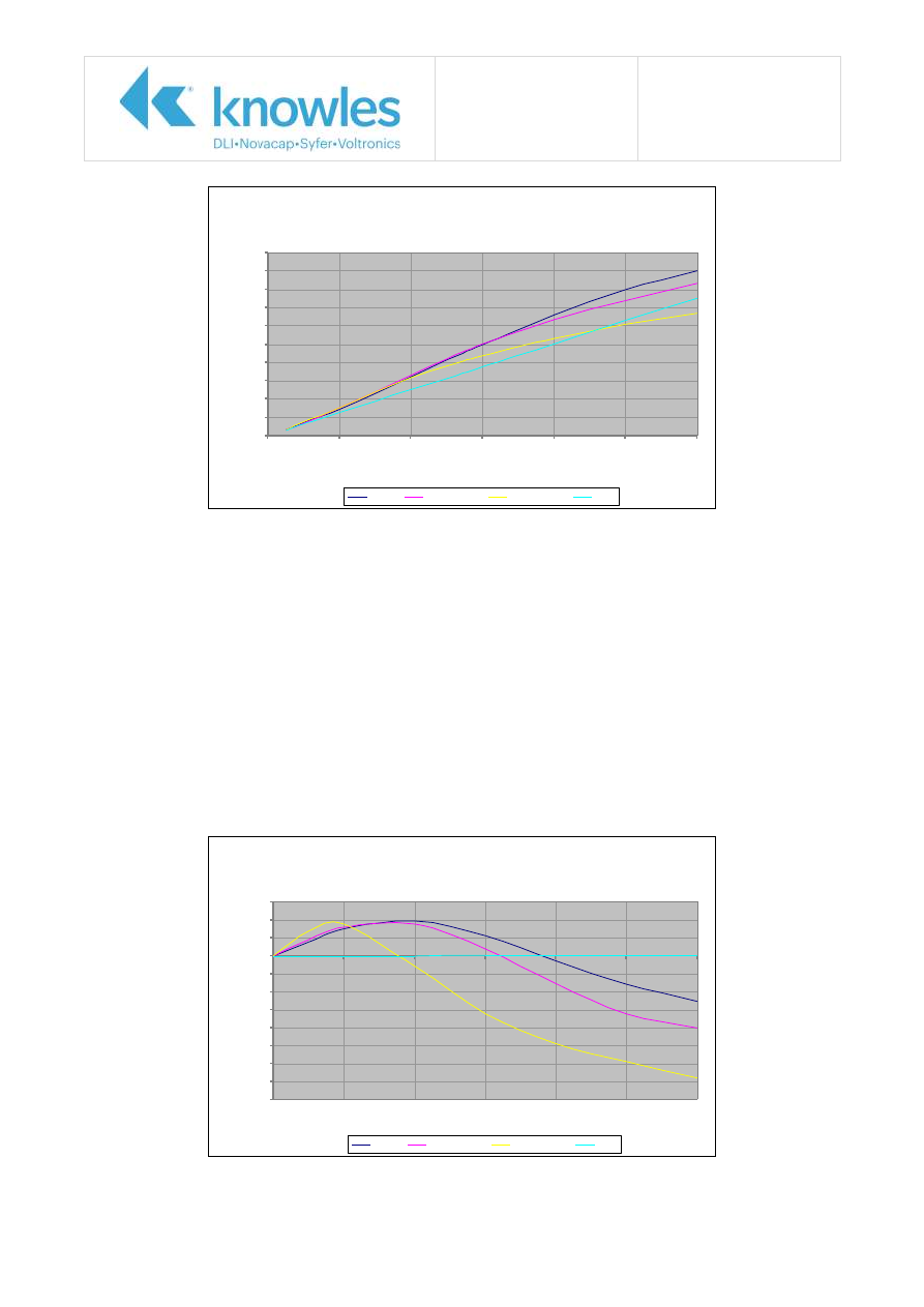
Application Note
Reference No: AN0033
AC250 Range Issue 8
Page 3 of 4
Approximate Current in mA per nF of Rated Capacitance
at 50Hz
0
0.01
0.02
0.03
0.04
0.05
0.06
0.07
0.08
0.09
0.1
0
40
80
120
160
200
240
VAC/Vrms(50Hz)
I/m
A
±30%
+30%-50%
+30%-80%
C0G
Fig.1
Values are typical and will vary with temperature and tolerance
Specific information regarding individual values may be available upon request, contact Syfer for more
details.
Ranges
Case sizes 0805 to 2220 are available in both X7R and C0G dielectrics with capacitances of up to
120nF. The capacitance ranges are divided into four groups, C0G which has negligible capacitance shift
with applied voltage and three subgroups of X7R, with ±30%, +30%-50% and +30-80% maximum
capacitance shift between 0V-240V 50Hz.
Below: Capacitance change with applied rms voltage at 50Hz. Capacitance was measured using an ART
AC Bias module connected to an HP4284A Precision LCR Meter. AC was supplied from 240V mains
source via a Claude Lyons LUC500 line voltage conditioner and an isolated variable transformer. These
graphs have been produced to define and distinguish between the separate ranges and designs
available. The values have been measured under a very specific set of conditions and may not be the
most suitable to calculate in circuit behaviour. For circuit simulation it is recommended that the current
values in fig. 1 are used.
Typical Measured Capacitance Change with Applied
Voltage
-80%
-70%
-60%
-50%
-40%
-30%
-20%
-10%
0%
10%
20%
30%
0
40
80
120
160
200
240
Voltage/Vrms(50Hz)
%
C
a
p
a
c
it
a
n
c
e
C
h
a
n
g
e
±30%
+30%-50%
+30%-80%
C0G
Fig. 2 Values are typical and will vary with temperature and tolerance

Application Note
Reference No: AN0033
AC250 Range Issue 8
Page 4 of 4
Capacitance Shift
0-240VAC 50Hz
Capacitance Values
Case Size
0805
1206
1210
1808
1812
2220
C0G
negligible shift
1.0pF – 470pF
1.0pF – 1.2nF
4.7pF – 2.2nF
4.7pF – 2.2nF
10pF – 5.6nF
10pF – 10nF
X7R ±30% max shift
560pF - 1.5nF
1.5nF – 10nF
2.7nF – 22nF
2.7nF – 22nF
6.8nF – 56nF
12nF – 120nF
X7R +30%-50% max shift
1.8nF – 3.3nF
12nF
27nF
27nF
68nF – 82nF
-
X7R +30%-80% max shift
3.9nF – 10nF
15nF – 47nF
33nF – 100nF
33nF – 100nF
100nF – 120nF
-
Fig. 3 Range Table
Ordering Information
The 250Vac Capacitors can be ordered by using a standard Syfer product code with the voltage code
A25.
Examples: 1206YA250473KXT or 2220JA250102JCT
1206
Case Size
Y
Polymer Termination FlexiCap™
A25
250V AC Rated up to 60Hz
0473 47nF Capacitance Value
K
10% Capacitance Tolerance
X
X - X7R Dielectric
T
Taped and Reeled
2220
Case Size
J
Nickel Barrier with Matte Tin Finish
A25
250V AC Rated up to 60Hz
0102 1nF
Capacitance Value
J
5% Capacitance Tolerance
C
C – C0G/NP0 Dielectric
T
Taped and Reeled
This Range is complementary to Syfer’s range of Surge and Safety Certified capacitors, Y2/X1 and X2
rated components are available in case sizes 1808, 1812, 2211, 2215 and 2220 with certifications from
TÜV and UL for standard terminations and our FlexiCap™ flexible polymer termination.
All other specifications and properties are as Syfer standard product.
For further information or technical assistance please contact our Sales Department on +44 1603
723310 or by email at

AN0035 Issue 3 - Magnetic Characteristics of Syfer Products
CN# P109825
Magnetic Characteristics of Syfer
Products
including Non Magnetic MLCC range
Multilayer Ceramic Capacitor (MLCC) Construction........................................2
Copper Barrier / Non-Magnetic ...............................................................3
Other Multi Layer Chip Capacitors (including Feedthrough Filters & X2Y) ......3
Radial Leaded Chip Capacitors ................................................................3
Planar Arrays & Discoidal Capacitors .......................................................4
Knowles (UK) Limited,
Old Stoke Road, Arminghall, Norwich,
Norfolk, NR14 8SQ, United Kingdom
Tel: +44 (0) 1603 723300
Tel. (Sales): 01603 723310
Fax: +44 (0) 1603 723301
www.knowlescapacitors.com/syfer
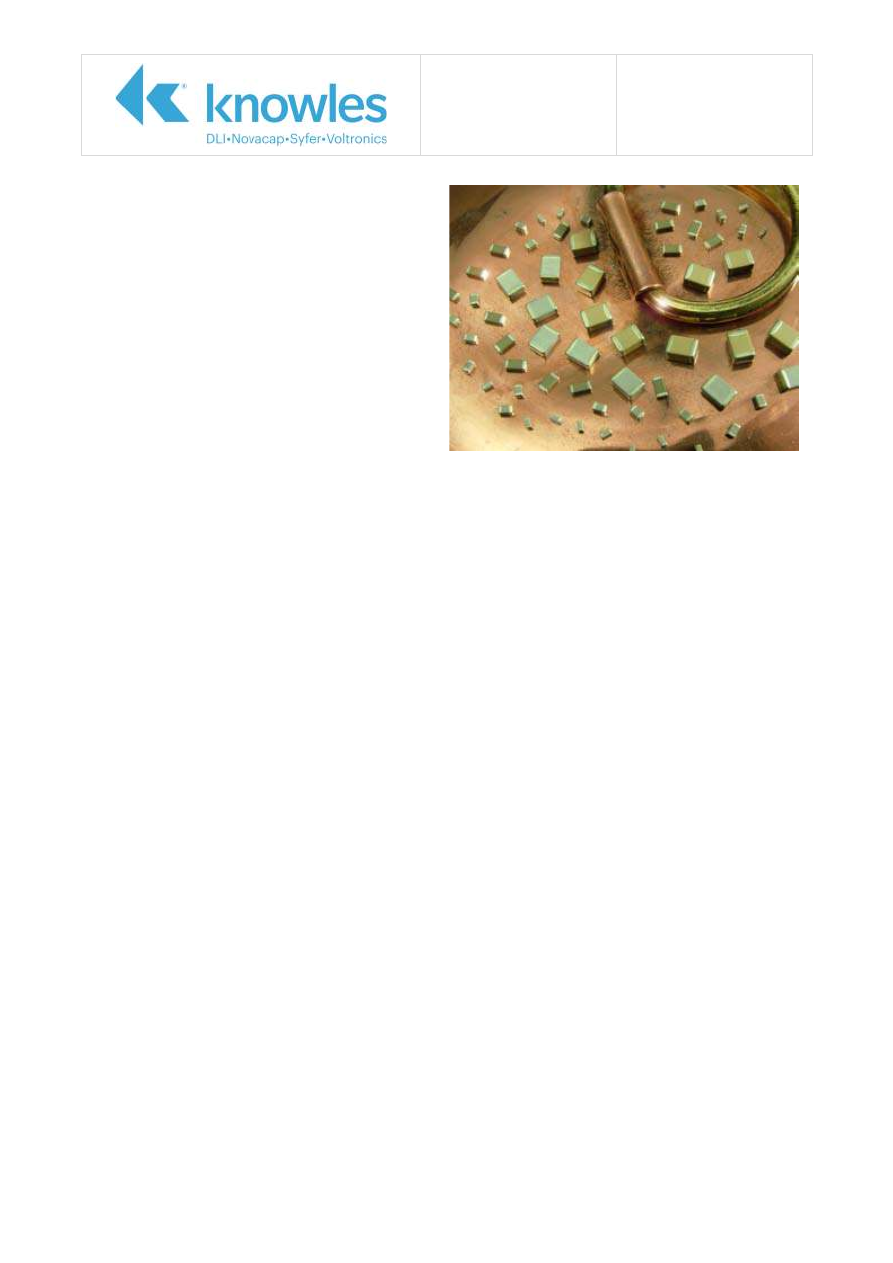
Application Note
Reference No: AN0035
Magnetic Characteristics
of Syfer Products Issue 3
Page 2 of 4
Introduction
All materials have electromagnetic properties,
defined by their relative permeability µ
r
, a ratio of
permeability relative to that of free space µ
0
. So a
µ
r
of 1.0000 is classed as totally non-magnetic. For
capacitive electronic components, the magnetic
characteristics can usually be ignored, but for
some applications such as in MRI scanners, the
magnetic characteristics must be considered.
Multilayer Ceramic Capacitor (MLCC) Construction
All ceramic MLCC based Syfer products consist of precious metal electrodes embedded in a dielectric
material, externally terminated to provide electrical contact using a conductive metal ink and / or
electroplated. The critical components we need to consider are the dielectric material and the
termination materials employed.
Dielectric
First, it is important to remember that the familiar designations X7R and C0G/NP0 are not
types of dielectric material, but simply define the characteristics of the material that is being
used. Most manufacturers, including Syfer, will use several dielectric materials in each class for
each designation. It is not therefore possible to simply discuss the magnetic properties of X7R
or C0G. Most dielectric materials have little or no magnetic permeability, but there are some
important exclusions. For example, certain C0G/NP0 types of dielectric contain Neodymium
Titanate and have a degree of magnetic permeability.
Termination
The common termination for MLCCs is electroplated Tin over Nickel onto a fired silver base
termination material. In this case the Nickel results in a significant degree of magnetism.
Alternative termination materials have always been available, the most common for
applications where the magnetism needs to be controlled being a precious metal based
consisting of alloys of Palladium, Silver and Platinum. The poor solder leach resistance of these
finishes resulted in a special solder alloy being developed especially to allow successful
soldering to them – 62Sn36Pb2Ag being a development of the then popular 63Sn37Pb or
60Sn40Pb Tin-Lead solder alloys.
Unfortunately, the restrictions imposed by RoHS regulations on the use of Lead in solders have
meant that these alloys are now banned in many applications and the replacements are almost
universally high tin content alloys – SAC (96.5Sn3Ag0.5Cu or very similar) being the most
popular. Palladium, Silver and Platinum alloys have poor solder leach resistance to Tin rich
alloys such as SAC and it has been necessary to look for alternative solutions.
Syfer have developed an electroplated Copper undercoat alternative to replace the Nickel for
magnetic critical applications. This Copper barrier layer allows for Lead free soldering with high
temperature 260
o
C soldering profiles as demanded by J-STD-020, without the termination
leaching associated with precious metal ink terminations. Copper barrier is available with
sintered terminations on selected C0G/NP0 dielectrics and with Syfer’s FlexiCap™ flexible
polymer termination on X7R dielectrics.
Application Note
Reference No: AN0035
Magnetic Characteristics
of Syfer Products Issue 3
Page 3 of 4
Individual Product Details
Copper Barrier / Non-Magnetic
The Copper barrier / non-magnetic range detailed on the Syfer website and in the MLCC catalogue is a
true non-magnetic range with a measured permeability µ
r
of approximately 1.0000
This range covers C0G/NP0, Syfer High-Q and X7R dielectrics and uses defined dielectric materials in
conjunction with copper barrier terminations to provide non-magnetic components with maximum
solder leach resistance, suitable for use with Lead free solders and soldering processes. The
termination system is also available with a SnPb plated finish for RoHS exempt applications
To identify the components from this range as non-magnetic, copper barrier, the termination code of
the part number is changed as below:
Description of Termination
Dielectric Base
Material
Termination
Code
Sintered silver base with copper barrier (100%
matte tin plating). RoHS compliant
C0G / NP0 & High Q
2
FlexiCap™ base with copper barrier (100% matte
tin plating). RoHS compliant
C0G / NP0, High Q &
X7R
3
Sintered silver base with copper barrier (tin/lead
plating). Non RoHS compliant
C0G / NP0 & High Q
4
FlexiCap™ base with copper barrier (tin/lead
plating). Non RoHS compliant.
C0G / NP0, High Q &
X7R
5
Special requests for other MLCC’s (e.g. Feedthrough chip filters) in non-magnetic dielectrics and with
copper plating can be considered – please refer requests to the factory.
Other Multi Layer Chip Capacitors (including Feedthrough Filters & X2Y)
The standard plated termination systems all have electroplated Nickel undercoat plating applied for
maximum soldering leach resistance. This imparts significant magnetism to the MLCC, with a typical
relative permeability µ
r
of 1.4000. This is irrespective of the dielectric material used.
Most Syfer MLCC’s can be supplied with non-plated precious metal terminations to reduce the magnetic
effect, however the dielectric material is not guaranteed to be non-magnetic for MLCC’s selected from
any range other than the specific non-magnetic range. In general, X7R dielectrics perform better than
C0G/NP0 dielectrics, but relative permeabilities up to typically µ
r =
1.0005 can be expected from certain
dielectrics when combined with non-magnetic terminations.
Radial Leaded Chip Capacitors
The lead material of radial sizes 8111 to 8141 inclusive is a steel base and obviously strongly
magnetic. Radial sizes 8151, 8161, 8165 & 8171 have tin plated copper leads. In all cases the chip
cannot be guaranteed to be non-magnetic. Nickel plated chips can be used in the assembly of all sizes
of standard component and variation may occur on a batch to batch basis.
The coating material used includes an Iron Oxide pigment to allow for laser marking of the component.
This has a minor magnetic effect – typical permeability of µ
r =
1.0040. This material is the most
common coating material used for leaded devices and as such is known to be in use in magnetic
sensitive applications, but it is the responsibility of the customer to determine if it is acceptable.

Application Note
Reference No: AN0035
Magnetic Characteristics
of Syfer Products Issue 3
Page 4 of 4
We can consider special requests for non-magnetic radial leaded components where the chip can be
controlled and plated copper leads specified. However, the gold colour powder coating cannot easily be
substituted. It has to remain the responsibility of the customer to confirm that the powder coating is
sufficiently non-magnetic for application. We can support with samples if required.
Planar Arrays & Discoidal Capacitors
The same considerations for the dielectric material apply as for MLCCs above. In general C0G/NP0
dielectrics in planar and discoidal components are of the magnetic variety with permeabilities of
typically µ
r =
1.0005.
The standard plating finish on these components is electroless plated Gold over electroless Nickel.
Tests have shown this to have very little if any magnetic effect, but please refer to the factory for any
non-magnetic application of these components.
EMI Filters
These are assembled using the above discoidal / planar capacitors soldered into plated brass bodies
with plated brass through pins.
Although the capacitor element is typically low or non-magnetic, special non-magnetic brass is not
used for standard components
Obviously the use of ferrite inductors in L-C, T & Pi filters infers considerable magnetism and cannot be
considered for non-magnetic filters.
For further information or technical assistance please contact our Sales Department on:
+44 1603 723310 or by Email at

AN0036 Issue 4 - High Q/Low ESR Capacitors
CN# P109825
High Q and Ultra Low ESR
Capacitor Ranges
Q and ESR Values – Standard Syfer MS Range .............................................4
ESR Values – Ultra Low ESR Range .............................................................6
Knowles (UK) Limited,
Old Stoke Road, Arminghall, Norwich,
Norfolk, NR14 8SQ, United Kingdom
Tel: +44 (0) 1603 723300
Tel. (Sales): 01603 723310
Fax: +44 (0) 1603 723301
www.knowlescapacitors.com/syfer
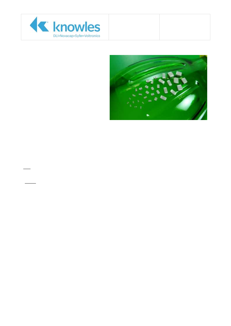
Application Note
Reference No: AN0036
High Q/Low ESR
Capacitors Issue 4
Page 2 of 9
Introduction
There are many different types of capacitor
with many different parameters; each is suited
to a range of applications. As operational
frequency requirements increase the most
important parameters are Q, Quality Factor,
and ESR, Equivalent Series Resistance. Syfer
Technology
Ltd
have
two
ranges
of
components, our High Q or MS range which
exhibits a high quality factor and low ESR and
our Ultra Low ESR range which has an
enhanced performance level, which are
designed for use in a variety of high frequency
applications such as telecommunications PAs,
microwave circuitry and RF modules. Non
magnetic versions of the MS type are also
available for use in applications such as MRI tuning; see our application note AN0035 for details.
Q, ESR and Power
Q is the Quality factor; it is the reciprocal function of the dissipation factor, DF, and represents the
losses of the capacitor. The higher the Q, the lower the DF and therefore, the lower the loss. ESR is the
Equivalent Series Resistance and represents the effective resistance to RF current; it encompasses
both the loss properties of the dielectric and electrode.
DF
1
Q
Q is Quality Factor, DF is Dissipation Factor
fC
2
1
X
c
X
c
is Capacitive Reactance in Ohms, f is frequency in Hertz and C is capacitance in
Farads
c
s
DF.X
R
R
s
is Equivalent Series Resistance in Ohms, DF is Dissipation Factor and X
c
is Capacitive
Reactance in Ohms
R
I
P
2
P is Power dissipated in the capacitor in Watts, I is RMS current in Amps and R is R
s
in
Ohms
Different dielectric and electrode combinations will exhibit different levels of Q and ESR, at lower
frequencies the dielectric material is the dominant factor, metal losses become more important at
higher frequencies. X7R materials are utilized at low frequencies and typically have a DF of around 1%
to 2%, this corresponds to a Q factor of 50 to 100, C0G/NP0 materials have a Q of around 600 to 1000
whilst Syfer’s High Q capacitors are broadly defined as Q>2000 at 1MHz.
100% measurement of Q is not practical above 1MHz, Capacitance bridges and LCR meters are not
accurate enough and when combined with leads and contacts rapid high frequency measurement is not
possible. It is necessary however to assess the Q and ESR at frequencies nearer to those which the
capacitor will encounter during operation. The most accurate method of determining Q and ESR at
elevated frequencies, 100MHz to 1.2GHz, is to use a resonant line coaxial jig. Syfer utilize the industry
standard Boonton 34A along with a Boonton 9241 RF voltmeter and an Agilent N2183A signal
generator as seen below. Higher frequency measurements are conducted on a shorter resonant coaxial
line system.
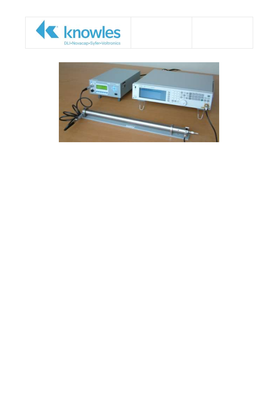
Application Note
Reference No: AN0036
High Q/Low ESR
Capacitors Issue 4
Page 3 of 9
Knowing the accurate value of ESR is important because it determines the suitability of the component
for use in RF power applications. If the ESR value is too high the self heating due to
R
I
P
2
losses will
be too great and the part will overheat and fail. The ESR also allows one to calculate the maximum
current rating for the component.
Worked Example:
A cellular phone base station, operating in the GSM900 band at 940MHz. The RF power is 40W and it is
a 50Ω system. The coupling capacitor is a MS 47pF 0805 with an ESR of approximately 0.088Ω at
940MHz. Using
R
I
P
2
where R = Z+ESR to find the circuit current gives 0.894A. To find the power
dissipated in the capacitor we put this value of current back into
R
I
P
2
where R=ESR which gives
0.0703W or 70mW. It is clear from this that the power dissipated in the capacitor can be simply
derived from the ratio of the ESR to the total circuit impedance multiplied by the system power,
(ESR/(Z+ESR))xP. For values of ESR significantly lower than the Z value there is a negligible impact on
the overall circuit impedance and it can be ignored leaving (ESR/Z)xP.
Using the same calculations for an Ultra Low ESR 0805 47pF, ESR 0.07 at 940MHz the power
dissipated in the capacitor is 56mW, a 20% reduction. This allows the system to run cooler or to be run
at higher power.
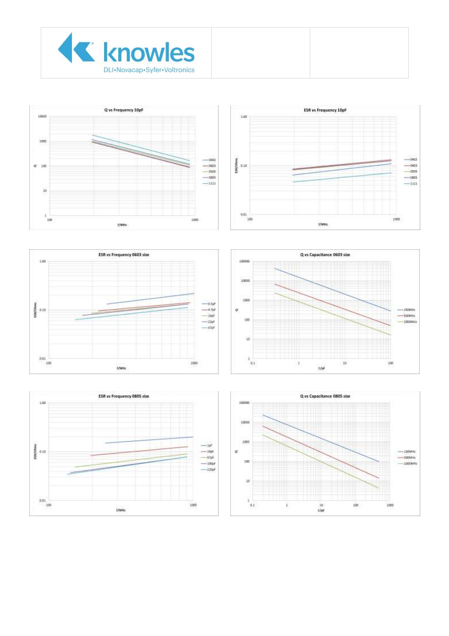
Application Note
Reference No: AN0036
High Q/Low ESR
Capacitors Issue 4
Page 4 of 9
Q and ESR Values – Standard Syfer MS Range
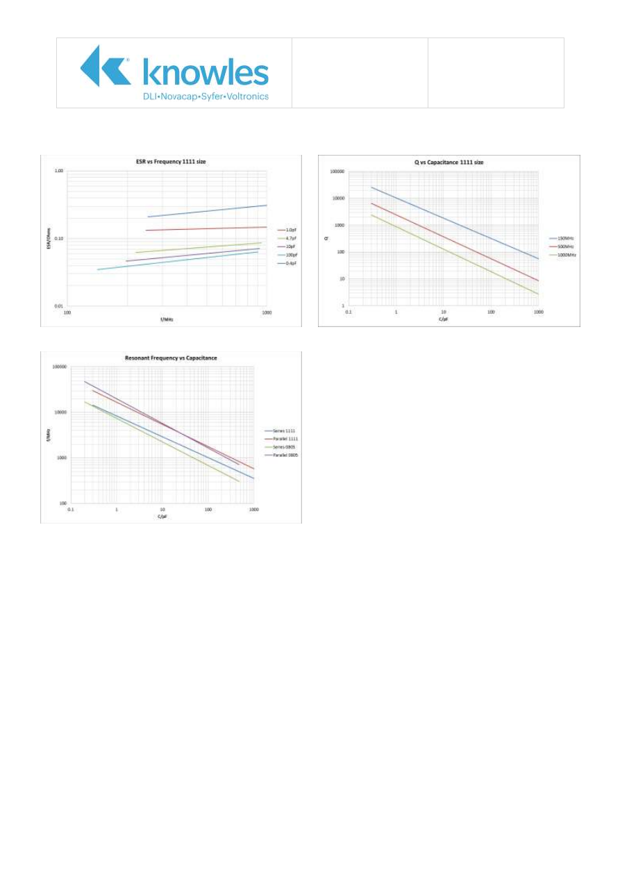
Application Note
Reference No: AN0036
High Q/Low ESR
Capacitors Issue 4
Page 5 of 9
Q and ESR Values – Standard Syfer MS Range (cont’d)
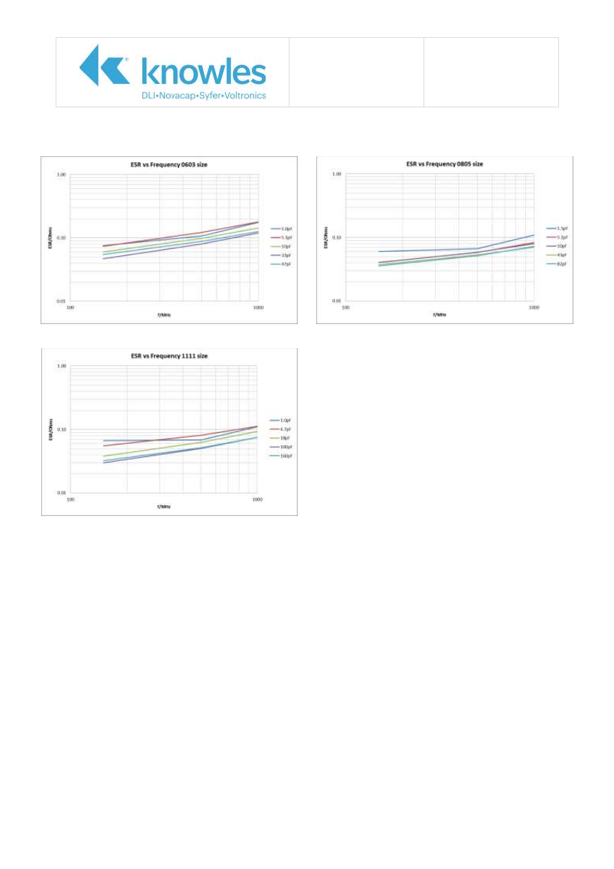
Application Note
Reference No: AN0036
High Q/Low ESR
Capacitors Issue 4
Page 6 of 9
ESR Values – Ultra Low ESR Range
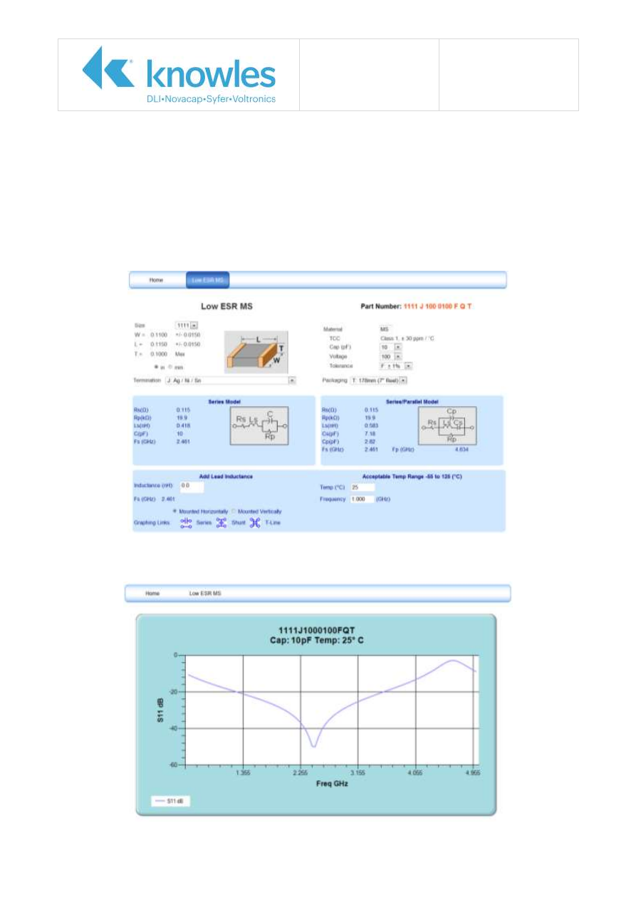
Application Note
Reference No: AN0036
High Q/Low ESR
Capacitors Issue 4
Page 7 of 9
CapCad™
Syfer's web based CapCad™ capacitor modelling software has been developed to provide customers
with an easy to use and readily accessible comparison tool for choosing the best Multilayer Capacitors
to suit the customer's needs. CapCad™ includes SPICE models with values that reflect typical
performance at the chosen frequencies and temperatures that are of importance to an application. The
user also has the ability to plot 2-port Scattering Parameters, Impedance, Q Factor or Equivalent
Capacitance over any frequency span from 1MHz to 40GHz while maintaining the ability to adjust the
temperature and note how it may affect the performance. CapCad™ also includes a Smith Chart utility
and the ability to copy the S-Parameter data in touchstone format (s2p). CapCad™ can be found on
the Syfer website under the technical information menu.
The graphing links allow the user to produce graphs of various parameters in both horizontal and
vertical mounting orientations.
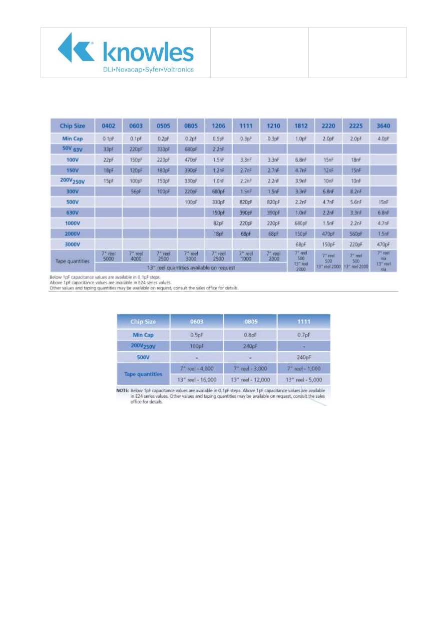
Application Note
Reference No: AN0036
High Q/Low ESR
Capacitors Issue 4
Page 8 of 9
Range
MS Range
U Range
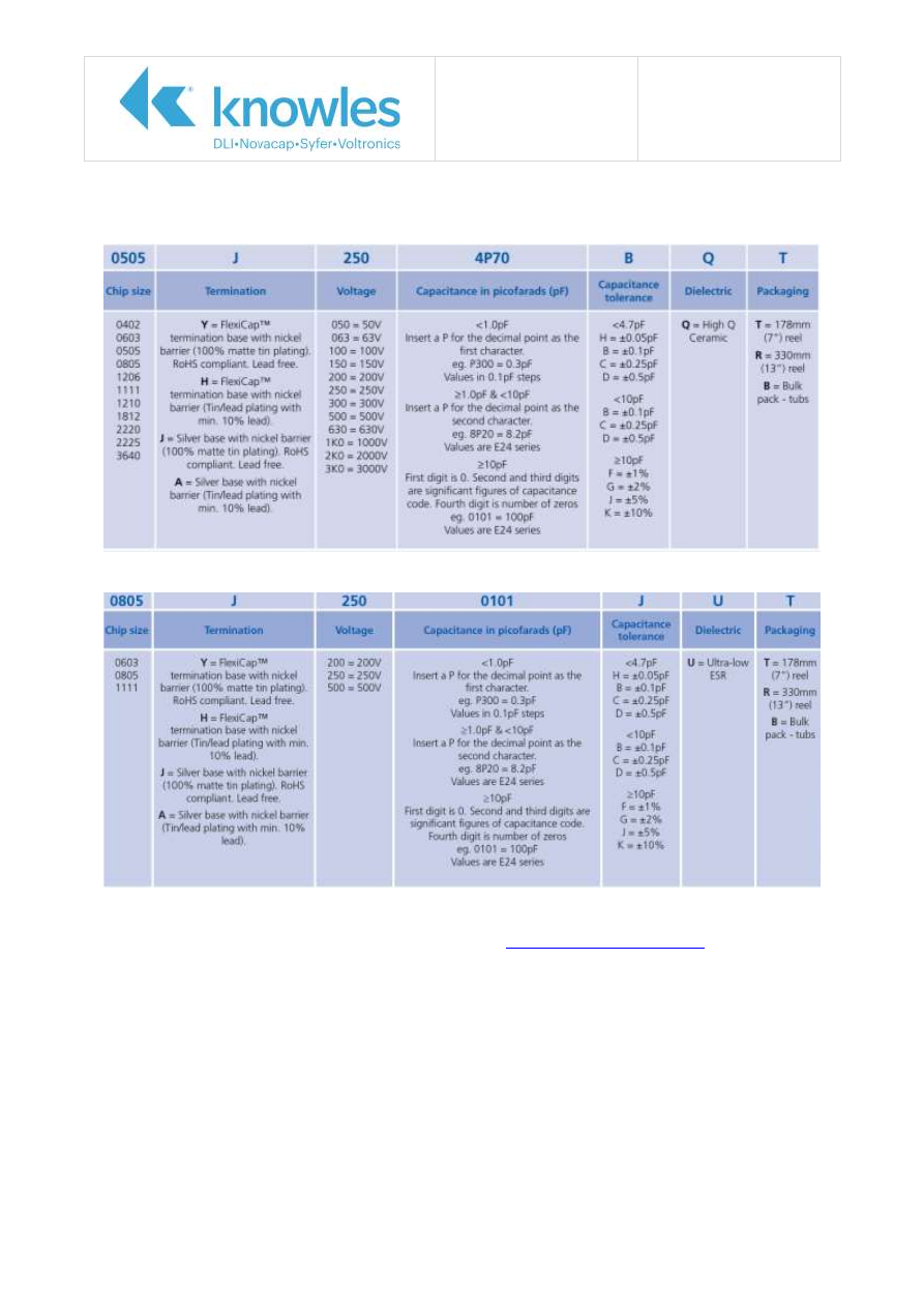
Application Note
Reference No: AN0036
High Q/Low ESR
Capacitors Issue 4
Page 9 of 9
Ordering Information
MS Range
U Range
For further information or technical assistance please contact our Sales Department on:
+44 (0)1603 723310 or by email at

AN0037 Issue 3 -
IECQ-CECC range of Capacitors
CN# P109825
IECQ-CECC range of Capacitors
Syfer Product Reliability Guide ...................................................................2
Periodic testing Carried out for Surface Mount MLCC .....................................4
Knowles (UK) Limited,
Old Stoke Road, Arminghall, Norwich,
Norfolk, NR14 8SQ, United Kingdom
Tel: +44 (0) 1603 723300
Tel. (Sales): 01603 723310
Fax: +44 (0) 1603 723301
www.knowlescapacitors.com/syfer
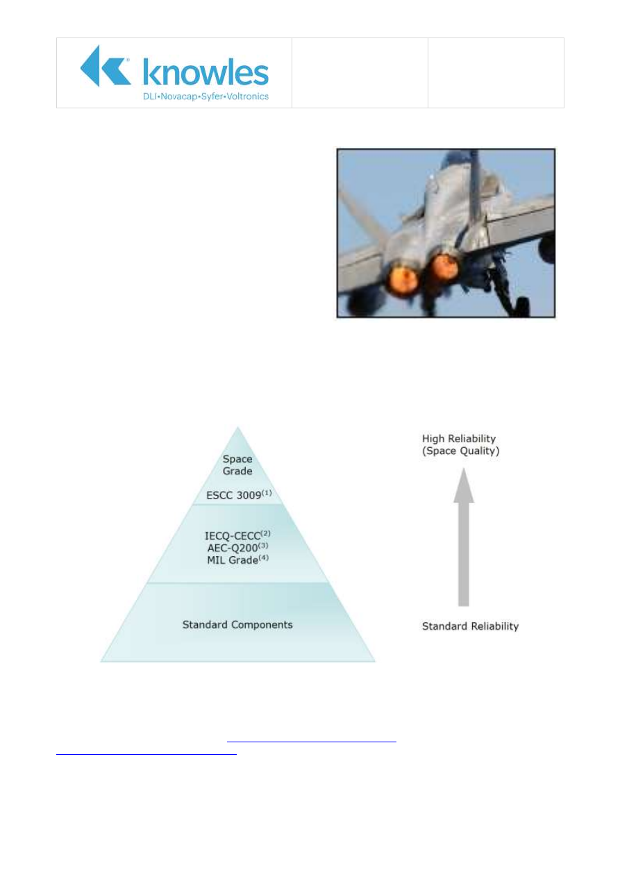
Application Note
Reference No: AN0037
IECQ CECC Capacitors
Issue 3
Page 2 of 6
Introduction
For applications such as Mil / Aerospace where
reliability is paramount, Syfer hold the IECQ-CECC
internationally recognised qualification for surface
mount ceramic capacitors tested in accordance with
the requirements of IECQ-CECC QC32100.
IECQ-CECC is the International Electrotechnical
Commission (IEC) Quality Assessment System for
Electronic Components and is a product quality
certification based on approval and routine periodic
testing of the range approved.
The IECQ-CECC standard offers customers an intermediate level of component quality, based on, but
above, commercial quality levels yet below space grade components. Component quality is checked
and demonstrated by sample test results, but parts are manufactured and tested using the same
processes and designs as commercial product. By comparison, space grade components usually include
conditioning tests and sample quality testing to be carried out on a batch basis, resulting in much
higher costs.
Syfer Product Reliability Guide
Notes:
(1) Space Grade tested in accordance with ESCC 3009. Refer to Syfer specification S02A 0100.
(2)
IECQ-CECC. The International Electrotechnical Commission (IEC) Quality Assessment System for
Electronic Components. This is an internationally recognised product quality certification. View
Syfer’s IECQ-CECC approvals at
http://certificates.iecq.org-syfer
www.knowlescapacitors.com/syfer
(3) AEC-Q200. Automotive Electronics Council Stress Test Qualification For Passive Components.
(4) MIL Grade. Released in accordance with US MIL standards available on request.

Application Note
Reference No: AN0037
IECQ CECC Capacitors
Issue 3
Page 3 of 6
Summary of Testing
IECQ-CECC approval is based on routine approval testing carried out either internally by Syfer or
independently at an external test laboratory.
Samples are taken from finished stock so as to be representative of standard build quality. All
components selected have been tested for
Visual
Dimensions
Capacitance and Dissipation Factor
Voltage Proof
Insulation Resistance
Destructive Physical analysis
Solderability
TCC (Temperature Coefficient of Capacitance) is also tested on a ceramic lot basis.
MLCC product is sampled on a quarterly rolling test program in accordance with the tables in below, 3
to 5 tests conducted each quarter, all tests conducted within 1 calendar year.
Samples are chosen to represent all case sizes covered by the approval and the sampling plan adjusted
to ensure that each test is not carried out on the same case size consecutively. The sample plan also
ensures that all approved voltage ratings are covered over a rolling program.
Samples are chosen to cover all product codes (product sizes) and both dielectric types (X7R & C0G)
over a rolling program
Where appropriate, the samples are tested after mounting on defined test boards. Following soldering,
the parts are cleaned through either aqueous or solvent cleaning plants to ensure no contamination
before testing commences.
Application Note
Reference No: AN0037
IECQ CECC Capacitors
Issue 3
Page 4 of 6
Periodic testing Carried out for Surface Mount MLCC
Test Ref
Year 1
Year 2
Year 3
Year 4
Q1 Q2
Q3
Q4
Q1 Q2
Q3
Q4
Q1
Q2
Q3
Q4
Q1
Q2
Q3 Q4
P1
16
1000
50
200
P2
16
1000
50
200
P3
16
1000
50
200
P4
16
1000
50
200
P5
50
200
16
1000
P6
50
200
16
1000
P7/P8
50
200
16
1000
P9
50
200
16
1000
P10
200
50
1000
16
P11
200
50
1000
16
P12/P13
200
50
1000
16
P14
1000
16
200
50
P15
1000
16
200
50
P16
1000
16
200
50
Test reference relates to below table. The figure in (brackets) is the sample size. The figures in the
table (16, 50 etc.) refer to the voltage of the parts under test.
Application Note
Reference No: AN0037
IECQ CECC Capacitors
Issue 3
Page 5 of 6
Test Ref
(qty)
Test
Termination
Type
Additional Requirements
Reference
P1 (77)
High Temperature
Exposure
(Storage)
All Types
Un-powered. 1000 hours @ T=150
o
C.
Measurement at 24 ± 2 hours after test
conclusion
MIL-STD-202
Method 108
P2 (77)
Temperature
Cycling
C0G: All types
X7R: Y & H only
1000 cycles -55
o
C to +125
o
C
Measurement at 24 ± 2 hours after test
conclusion
JESD22
Method JA-104
P3 (77)
Moisture
Resistance
All Types
T = 24 hours/cycle. Note: Steps 7a & 7b not
required. Un-powered.
Measurement at 24 ± 2 hours after test
conclusion
MIL-STD-202
Method 106
P4 (77+77)
Biased Humidity
All Types
1000 hours 85
o
C/85%RH. Rated voltage or
50V whichever is the less (77pcs) and 1.5V
(77pcs)
Measurement at 24 ± 2 hours after test
conclusion
MIL-STD-202
Method 103
P5 (77)
Operational Life
All Types
Condition D Steady State T
A
=125
o
C at full
rated.
Measurement at 24 ± 2 hours after test
conclusion
MIL-STD-202
Method 108
P6 (5)
Resistance to
Solvents
All Types
Note: Add aqueous wash chemical. Do not use
banned solvents
MIL-STD-202
Method 215
P7 (30
Mechanical Shock
C0G: All types
X7R: Y & H only
Figure 1 of Method 213. Condition F
MIL-STD-202
Method 213
P8 (30)
Vibration
C0G: All types
X7R: Y & H only
5g’s for 20 minutes, 12 cycles each of 3
orientations. Note: Use 8”X5” PCB .031” thick
7 secure points on one long side and 2 secure
points at corners of opposite sides. Parts
mounted within 2” from any secure point.
Test from 10-2000Hz
MIL-STD-202
Method 204
P9 (12)
Resistance to
Soldering Heat
All Types
Condition B, no pre-heat of samples: Single
Wave Solder – Procedure 2
MIL-STD-202
Method 210
P10 (30)
Thermal Shock
C0G: All types
X7R: Y & H only
-55
o
C/+125
o
C. Number of cycles 300.
Maximum transfer time – 20 seconds, Dwell
time – 15 minutes. Air-Air
MIL-STD-202
Method 107
P11 (27)
Adhesion, Rapid
Temp Change &
Climatic Sequence
X7R: A, F & J
only
5N force applied for 10s, -55
o
C/ +125
o
C for 5
cycles, damp heat cycles
BS EN132100
Clause 4.8,
4.12 & 4.13
P12 (30)
Board Flex
C0G: All types
X7R: Y & H only
3mm deflection Class I
2mm deflection Class II
AEC-Q200-005
P13 (12)
X7R: A, F & J
only
1mm deflection.
BS EN132100
Clause 4.9
P14 (30)
Terminal Strength
All Types
Force of 1.8kg for 60 seconds
AEC-Q200-006
P15 (30)
Beam Load Test
All Types
-
AEC-Q200-003
P16 (45)
Damp Heat
Steady State
All Types
56 days, 40
o
C/93%RH. 15
no volts, 15
5Vdc, 15
R
v
or 50V whichever is the less
BS EN132100
Clause 4.14
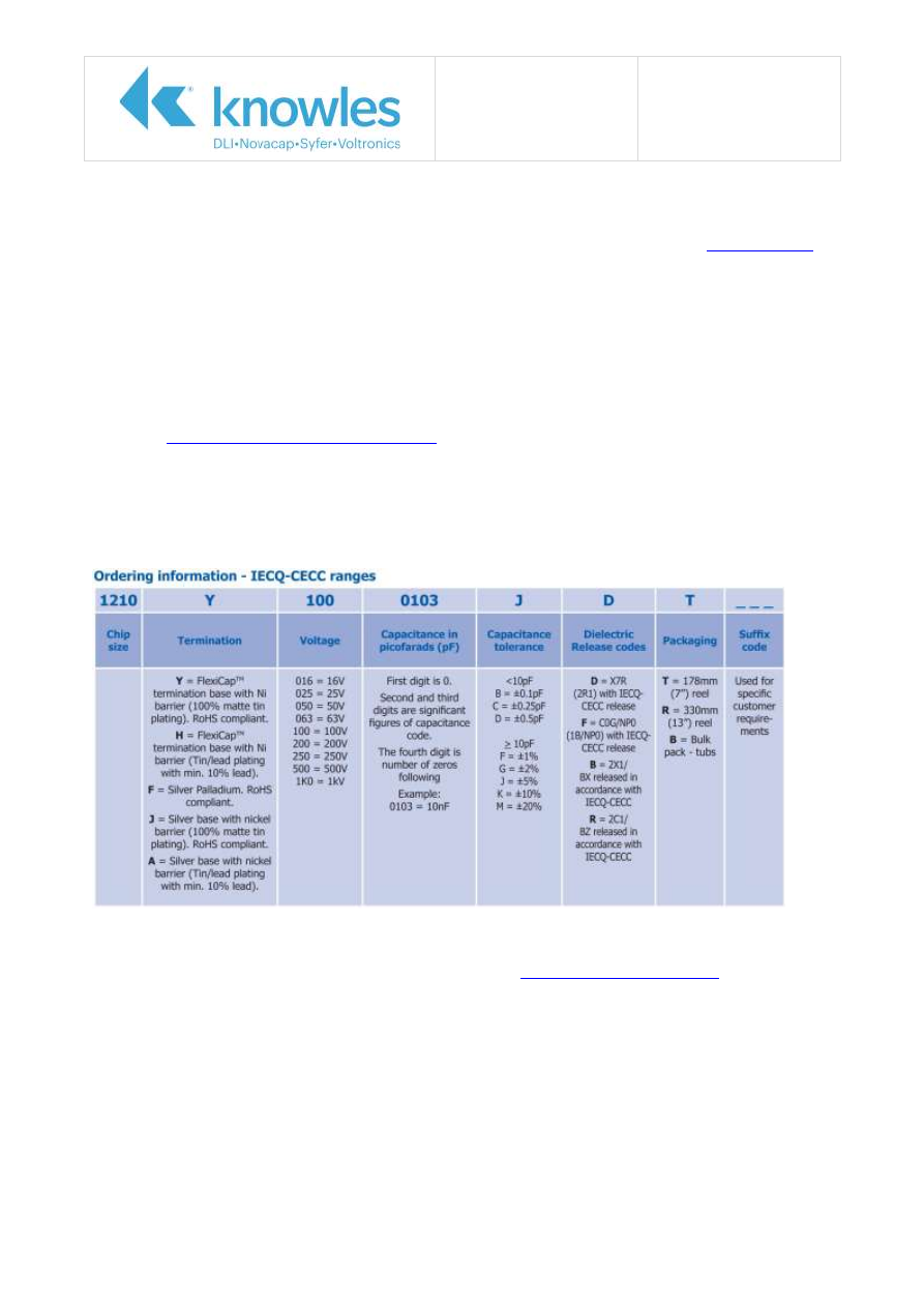
Application Note
Reference No: AN0037
IECQ CECC Capacitors
Issue 3
Page 6 of 6
Certificate Numbers
The following certificates are authorised by the International Electrotechnical Commission Quality
Assessment System for Electronic Components and can be viewed at their website
IECQ Certificate No.: Q-IECQ BSI 05.0003 / CB Certificate No.: M1043 IECQ
Certificate of Approval of Manufacturer
IECQ Certificate No.: Q-IECQ BSI 07.0002 / CB Certificate No.: E1281/F
Fixed Multilayer ceramic Capacitors
Part Numbering
Full details of the approved ranges can be found in the latest Syfer catalogues or by reference to the
Syfer website
www.knowlescapacitors.com/syfer
To identify approved MLCC parts, the dielectric code in the part number is changed from X to D (X7R)
and C to F (C0G) as per the example below. In addition, the controlled TCVC dielectric codes B (BX /
2X1) and R (BZ / 2C1) can also be used.
Always state on any PO that IECQ-CECC release is required
For further information on our AECQ-CECC approved ranges or for technical assistance please contact
our Sales Department on +44 1603 723310 or by Email at

AN0038 Issue 3 -
ProtectiCap™
CN# P109825
ProtectiCap™ Surface
Coated MLCC
Knowles (UK) Limited,
Old Stoke Road, Arminghall, Norwich,
Norfolk, NR14 8SQ, United Kingdom
Tel: +44 (0) 1603 723300
Tel. (Sales): 01603 723310
Fax: +44 (0) 1603 723301
www.knowlescapacitors.com/syfer
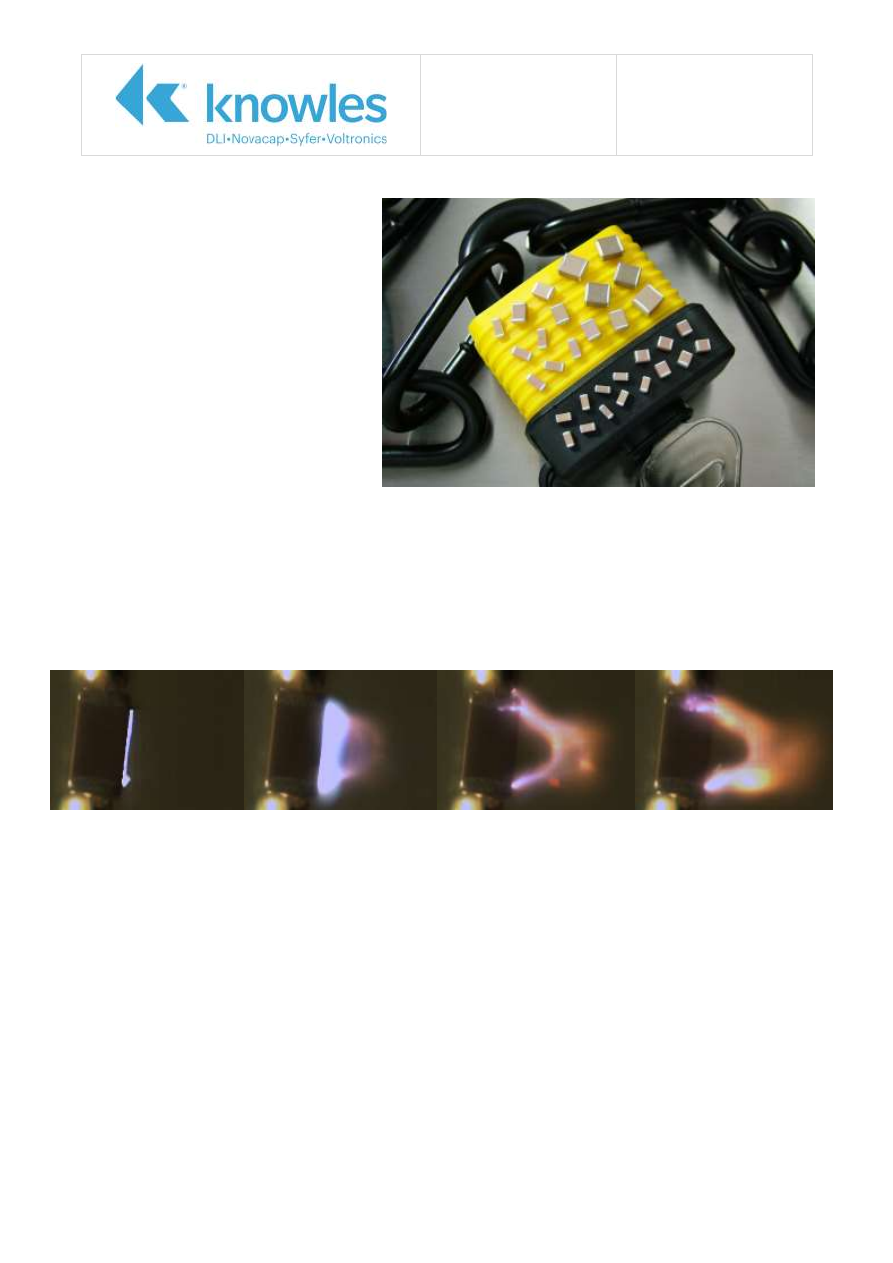
Application Note
Reference No: AN0038
ProtectiCap™ Issue 3
Page 2 of 6
Introduction
Syfer ProtectiCap™ high voltage, surface
mount, multi layer ceramic capacitors
are designed specifically to reduce the
occurrence of surface arcing in high
voltage applications. The range
incorporates 1206 to 2220 EIA case sizes
in voltages from 2kV to 5kV and enables
use without the need for conformal
coating post soldering. The addition of
the ProtectiCap™ range maintains Syfer’s
position as world leader in high voltage
MLCC with parts such as a 1206 3kV
1.5nF now available. ProtectiCap™
capacitors should provide benefits in
power supply, lighting ballast, inverter,
voltage multiplier and many other high
voltage applications
Surface Arcing
Surface arcing, arc-over, flash-over, corona discharge, these are all terms for the same thing, an
undesirable high voltage discharge which can cause interference and/or component failure. Surface
arcing occurs when the dielectric strength of the surface environment is exceeded. High potential
difference between the opposing terminations can lead to partial ionisation of the air which can then
break down completely and allow a spark to discharge, this spark is visible, audible and the associated
corona discharge will create electrical noise.
Pictures showing the propagation of surface arc.
The arc inception voltage is the voltage at which arcing will commence, there are several factors which
can affect this.
1.
Humidity. At levels of high humidity surface arcing is more prevalent, this explains the
sometimes seasonal nature of arcing problems and also why there are more issues in
geographical areas of high humidity.
2.
Surface Contamination. Solder balls, flux residue and other contaminents which have been
deposited during manufacturing, processing and assembly.
3.
Dielectric Type. Higher dielectric constant materials are more susceptible, also higher
capacitance values. C0G/NP0 is not usually affected.
4.
PCB design. Oversize pads, vias underneath capacitors, buried layers and geometries which
inhibit good cleaning can all contribute to arcing problems.
To combat surface arcing pads should be well spaced and not have sharp corners and PCBs should be
cleaned post soldering. Environmental factors such as humidity are more difficult to control which is
why most vendors’ high voltage MLCC may require the PCB to be conformal coated.
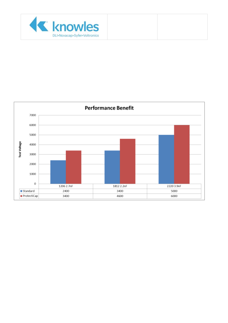
Application Note
Reference No: AN0038
ProtectiCap™ Issue 3
Page 3 of 6
ProtectiCap™ provides consistent performance advantages without the need for confomal coating of
the PCB. Syfer employ a unique set of processes to apply a low permittivity glass coating to an already
optimised high voltage MLCC design. The sealed, smooth finish and low dielectric constant allows for
higher voltages and capacitance values in smaller case sizes, a prime example of this is the
1206P3K00102KXT which would previously only have been available in an 1808 case size.
Summary of Testing
Syfer have undertaken a significant program of testing in order to evaluate the performance of the
ProtectiCap™ range. The minimum arc inception voltage has been evaluated across the range and
shows an improvement in performance of a minimum of 1000V over standard parts.
Arc Voltage Evaluation
The above shows the performance benefit with respect to surface arcing in bulk testing across the
range of sizes. The tests were performed on Syfer line testers and the graph shows the maximum test
voltage before any arcing occurs. Voltage was supplied instantaneously with a current limit of 50mA.
Qualification Testing
In order to verify the reliability and consistency of performance of the ProtectiCap™ range a test
regime has been assembled based on our extensive knowledge of high reliability products. Standard
test methods have been employed from various international specifications including AEC-Q200, IECQ-
IECC and MIL standards. The table below shows the tests, methods, criteria and results with the
ProtectiCap™ parts meeting all requirements.
Application Note
Reference No: AN0038
ProtectiCap™ Issue 3
Page 4 of 6
Test
Reference
Sample Size
per Lot
Accept on
Number
Failed
Additional Requirements
Result
J-STD-020D
Moisture/Reflow
Sensitivity
Classification for Non-
Hermetic Solid State
Surface Mount Devices
25
0
1.24hr bake @ 125degC. 2.Moisture
soak for 168hre 85/85. 3.PCB
assembly (3X260deg reflow).
4.External Visual. 5.Electrical Test
Pass
AEC-Q200 test 3.
High Temp
Storage
MIL-STD-202
method 108
77
0
Unpowered 1000 hours @ 150°C.
Pass
AEC-Q200 test 4.
Temperature
cycling
JESD22
method JA-104
77
0
1000 cycles (-55°C to 125°C)
Pass
DPA
EIA-469
50
0
25 width/25 length
Pass
Moisture
Resistance
MIL-STD-202
method 106
77
0
t = 24 hours/cycle. Unpowered.
Pass
Biased Humidity
MIL-STD-202
method 103
77
0
1000 hrs 85°C/85%RH. 1.5 Vdc and
Rated Voltage.
Pass
Operational Life
MIL-STD-202
method 108
77
0
Rated Voltage @ 125°C.
Pass
External Visual
MIL-STD-883
method 2009
<1812 = 125
1812 = 200
>1812 = 315
0
Inspect device construction and
workmanship. Electrical test not
required.
Pass
Physical
dimensions
JESD22
method JB-100
5
0
Verify physical dimensions to the
device specification.
Pass
Mechanical shock
MIL-STD-202
method 213
30
0
Figure 1 of method 213 SMD:
Condition F.
Pass
Vibration
MIL-STD-202
method 204
30
0
5 g's for 20 min., 12 cycles each of 3
orientations. Test from 10-2000Hz.
Pass
Resistance to
Soldering Heat
MIL-STD-202
method 210
30
0
Condition B No pre-heat of samples.
Pass
Thermal Shock
MIL-STD-202
method 107
30
0
(-55/+125°C). 300 cycles. Max
transfer time: 20 s. Dwell time: 15
minutes. Air-Air.
Pass
Solderability
J-STD-002
(JESD22-B102)
15
0
Aged solderability test. Use dry heat.
150 °C for 16 hrs.
Pass
Syfer standard
solderability test
IEC 60068-2-58
test Td
5
0
Immersion in 60/40 (Sn/Pb) solder at
235 ± 5
o
C for 2 ± 0.5 seconds.
Coverage shall exceed 95%.
Pass
Electrical
characteristics
Standard Syfer 100%
electrical
200-400 units
0
As per standard Syfer test conditions.
Pass
Board flex
AEC-Q200-005
30
0
3 mm deflection Class I 2
mm deflection Class II
Pass
Terminal
strength
AEC-Q200-006
30
0
Force of 1.8kg for 60 seconds
Pass
Beam Load Test
AEC-Q200-003
30
0
Pass
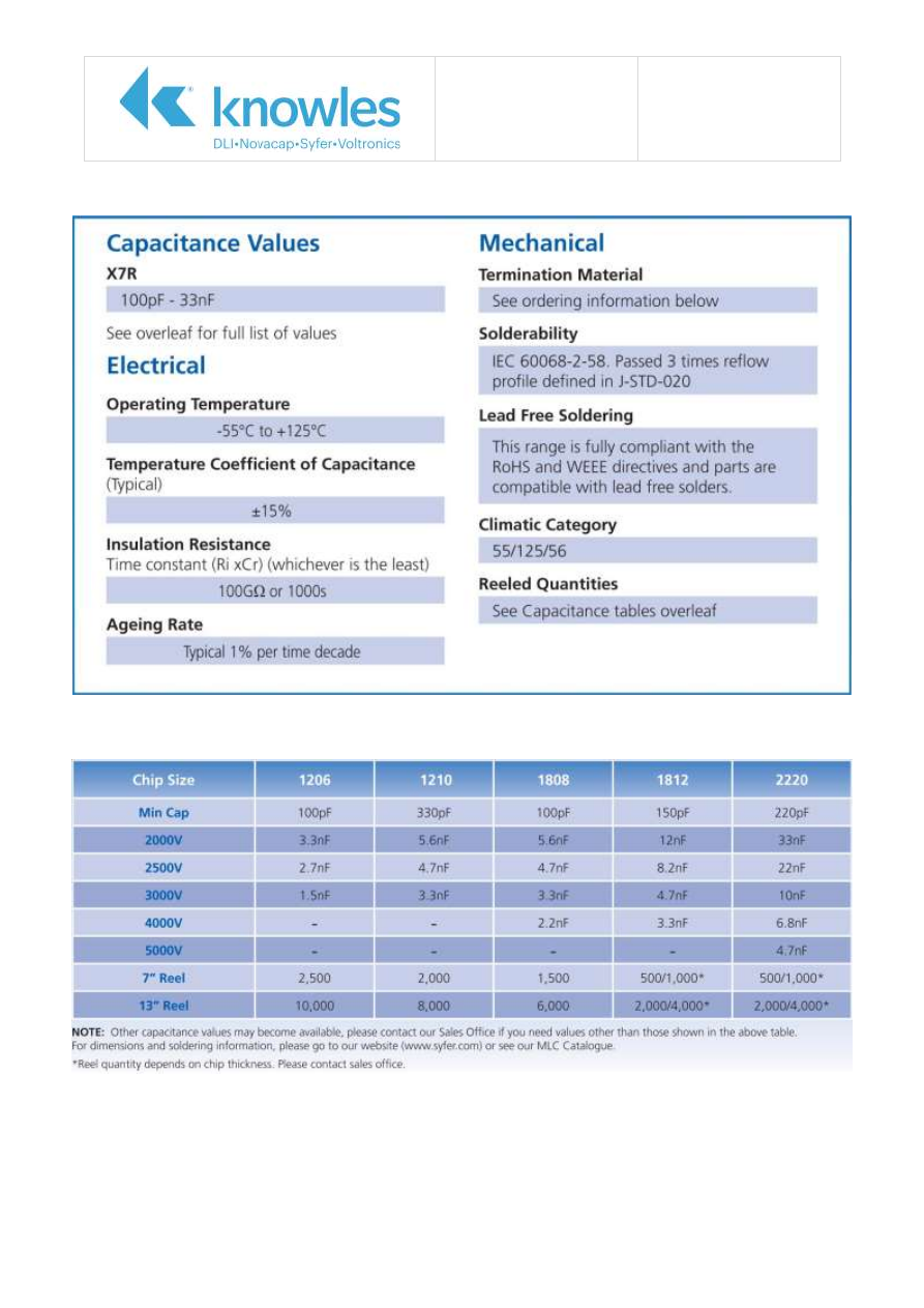
Application Note
Reference No: AN0038
ProtectiCap™ Issue 3
Page 5 of 6
Range
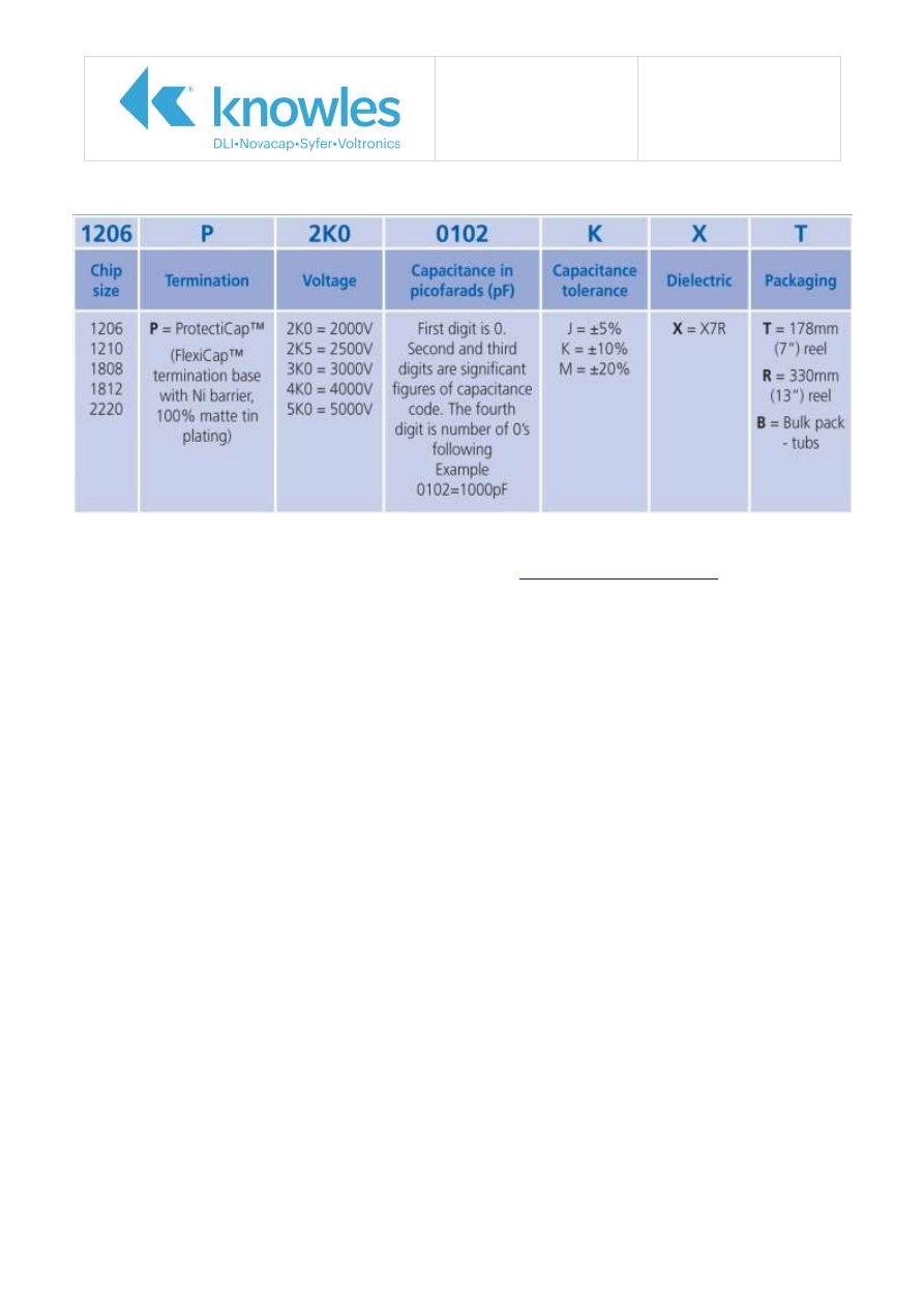
Application Note
Reference No: AN0038
ProtectiCap™ Issue 3
Page 6 of 6
Ordering Information
For further information on our ProtectiCap™, other ranges, or for technical assistance please contact
our Sales Department on +44 1603 723310 or by email at

AN0039 Issue 4 - StackiCap™
CN# P109825
StackiCap™ High Voltage
High CV MLCC
The Technology Behind StackiCap™ ...........................................................4
Range and Ordering Information ................................................................7
Knowles (UK) Limited,
Old Stoke Road, Arminghall, Norwich,
Norfolk, NR14 8SQ, United Kingdom
Tel: +44 (0) 1603 723300
Tel. (Sales): 01603 723310
Fax: +44 (0) 1603 723301
www.knowlescapacitors.com/syfer
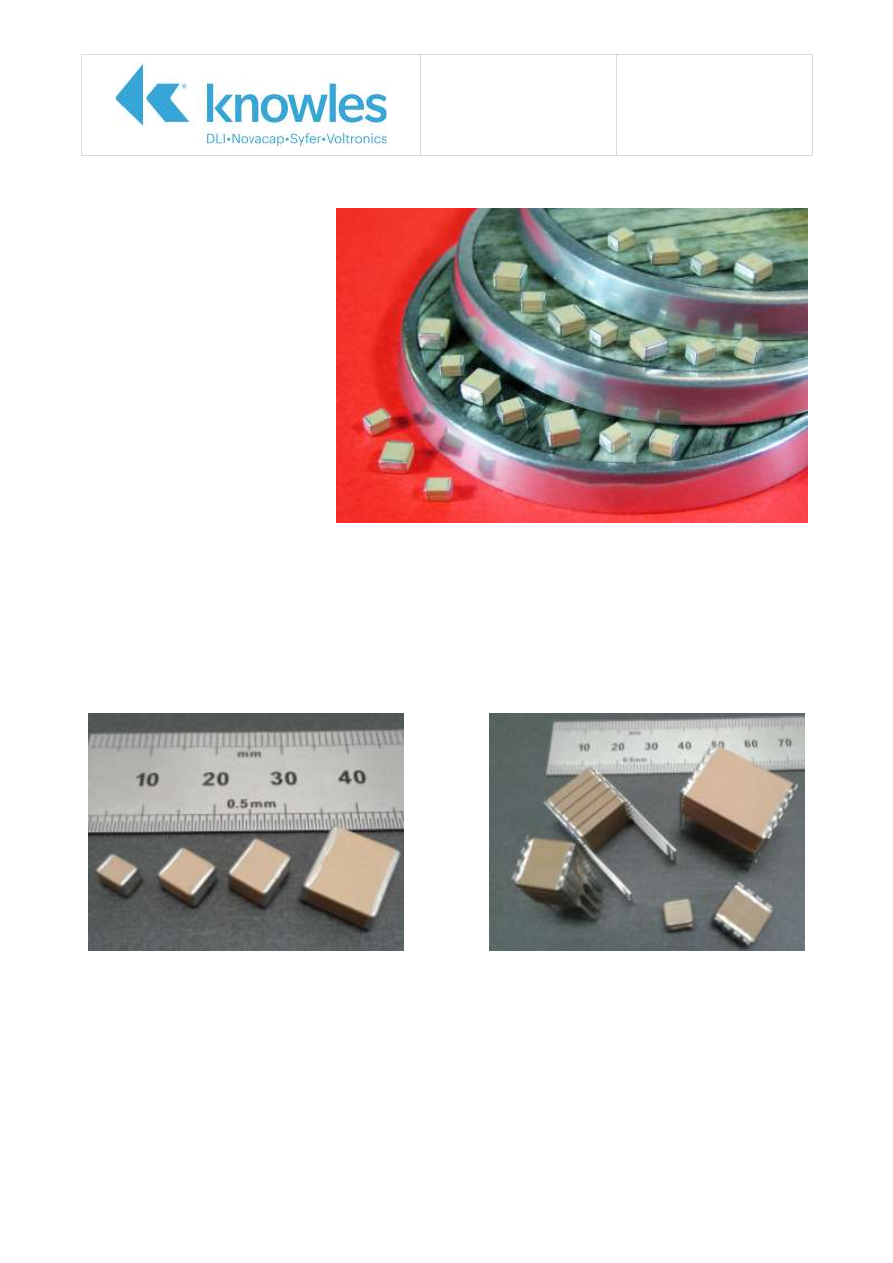
Application Note
Reference No: AN0039
StackiCap™ Issue 4
Page 2 of 7
Introduction
Syfer StackiCap™ surface mount
MLCs are designed to provide high
CV in compact packages and offer
the greatest volumetric efficiency
and CV per unit mass of any high
voltage X7R ceramic capacitors
available. Syfer has conceived,
developed and protected, GB Pat.
App. 1210261.2, a unique process
in order to deliver this
groundbreaking product. Combined
with FlexiCap™ stress relieving
terminations these parts have the
potential to replace film and
tantalum capacitors and make
many stacked products obsolete.
StackiCap™ are suitable for a
plethora of applications such as
switch mode power supplies for filtering, tank and snubber, DC-DC converter, DC block, voltage
multipliers etc. and will provide huge benefits in applications where size and weight is critical. At this
moment 1812,2220 and 3640 case sizes have been launched and are commercially available,
additional sizes up to 8060 are still under development, please see the Syfer website or contact the
factory for the latest ranges.
Downsizing Potential
Offering significant increases in available capacitance StackiCap™ can offer significant downsizing over
existing technology, below are some images showing the benefits.
Fig 1. StackiCap sizes 1812 to 3640
Fig 2. Various stacked assemblies up to 8060 5 stack
Figure 1 shows the initial StackiCap™ product range sizes of 1812, 2220, 2225 and 3640. 5550 and
8060 development sizes are not shown. Figure 2 shows a range of stacked and stacked leaded
assemblies of sizes 2225, 3640, 5550 and 8060 up to a maximum of 5 in a stack. Figures 3 and 4
show examples of what can be replaced with a single StackiCap™ component. In the most extreme
cases an 8060 1kV 470nF could be replaced with a single 2220 1kV 470nF and a 3640 1kV 180nF could
be replaced with a single 1812 1kV 180nF, these are 10:1 and 7:1 footprint reductions respectively.
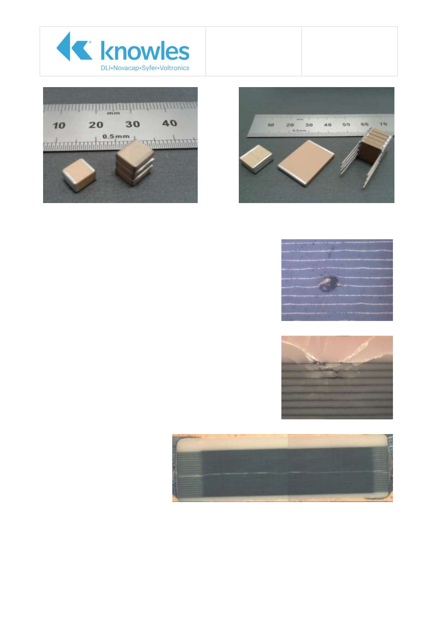
Application Note
Reference No: AN0039
StackiCap™ Issue 4
Page 3 of 7
Fig 7. Piezo stress crack failure
Fig 3. 2220 500V 1µF StackiCap™ & 2225 3 Stack
500V 1µF
Fig 4. 3640 500V 3.3µF StackiCap with 8060 and
3640 5 stack alternatives
Historical Limitations
The limits of design are defined by the failure modes and there are
many failure modes which limit the extent to which mid to high
voltage MLCC can be developed. There are extrinsic failure modes
such as mechanical and thermal cracking but we will look at the
intrinsic ones which are in the hands of the manufacturer. The
limiting factor for MLCC has changed over time, early MLCC were
limited mainly by the quality and purity of the dielectric materials
themselves with point defects and contamination, fig 5, limiting
the maximum number of layers and the minimum thickness of
those layers. As dielectric materials and materials preparation and
processing improved the limiting factor became the dielectric
strength of the material itself. Once this point had been reached
one could imagine that thicker and larger parts could be
manufactured without fear of dielectric breakdown, fig 6, or point
failures, however a new failure mode appeared, electro-
mechanical stress cracking. Commonly referred to as piezo electric
it can also follow electrostrictive behaviour, see fig 8. This is the
failure mode that has been the limiting factor for MLCC
manufactures for some time now, it affects most class II barium
titanate base dielectrics and becomes an issue for larger size,
1210 upwards, and higher voltage, 200V upwards components.
The crack typically runs through the centre of the component
along one or two dielectric layers, fig
7. Most solutions involve stacking
capacitors together with lead frames
in order to increase the available
capacitance for a given footprint but
this is labour intensive, costly and
can lead to other reliability issues.
Other solutions involve special
dielectric formulations but these are
usually a trade off for dielectic constant and therefore the ultimate capacitance value available.
Fig 5. Contamination defect
Fig 6. Dielectric breakdown
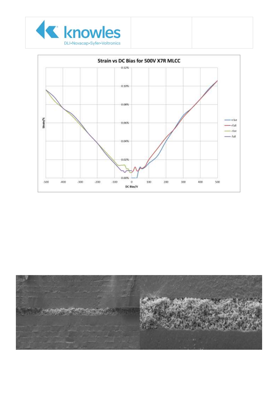
Application Note
Reference No: AN0039
StackiCap™ Issue 4
Page 4 of 7
Fig 8. An example of the mechanical response of an X7R MLCC under DC bias
The Technology Behind StackiCap™
After a series of trials and iterations Syfer have developed a single chip solution to electro-mechanical
failure limitation, StackiCap™. The novel and patent pending aspect, GB Pat. App. 1210261.2, is an
inbuilt stress relieving layer which allows the capacitor to exhibit the electrical and physical behaviour
of multiple, thinner, components whilst exploiting the manufacture and process benefits of being a
single unit. The stress relieving layer is made up of a combination of already utilised material systems
and is formed during the standard manufacturing process. The layer is positioned in the place/s where
mechanical stress is the greatest allowing for mechanical decoupling of the multiple component layers
with 2,3 and 4 “stack”versions trialled at this point.With FlexiCap™ flexible termination material and no
need to attach components together to form a stack there is no need for a lead frame allowing for
standard tape and reel packaging with pick and place capability.
Fig 9. SEM Micrograph of fracture sections showing the stress relieving “spongy” layer

Application Note
Reference No: AN0039
StackiCap™ Issue 4
Page 5 of 7
Qualification Program
StackiCap™ technology has been under development at Syfer for some time, parts and materials have
been subjected to Syfer’s standard quality control and reliability regime, this is detailed below:
1.
Material Verification (before use)
All materials are inspected in accordance with defined specifications before being accepted for. For
example, each new lot of dielectric powder is subjected to:
Powder size distribution analysis on milled ink.
Solids content and viscosity analysis of the subsequently manufactured ink.
Capacitor approval batch manufacture to perform:
Internal Destructive Physical Analysis examination.
Electrical tests for Capacitance, Dissipation Factor, Insulation Resistance and Dielectric
Withstand Voltage.
Dielectric Constant measurement.
Endurance tests conducted at 125
C with 1.0 or 1.5x rated voltage applied.
TCC measurements
85/85 tests.
2.
Product Verification (during and after manufacture)
As part of Syfer’s standard production process each batch is subjected to a series of inspection and
testing stages during which the quality of the product is examined and verified. These stages
include:
Dielectric thickness measurements using lasers during the capacitor construction process.
Internal Destructive Physical Analysis. A sample of capacitors is taken from each batch and
subjected to an internal visual examination to verify the capacitor construction.
Plating thickness measurements conducted using the X-Ray Fluorescence method.
Solderability and leach tests conducted by immersing capacitors into solder.
100% production electrical tests for Capacitance, Dissipation Factor and Dielectric Withstand
Voltage.
These inspection and test stages are supported by:
Visual inspection stages conducted throughout the manufacturing process.
Statistical Process Control.
Final QC Inspection.
3.
Routine Reliability Tests
In addition to the standard inspection and tests performed during batch manufacture, a sample of
batches is also randomly selected for additional routine endurance, humidity and bend tests.
Reliability tests are also conducted by external test laboratories as part of maintaining product
approvals and are also conducted at Syfer to assess long-term product performance.
The reliability tests conducted at Syfer include:
Life Test. Capacitors are subjected to 1000 hours at 125
C with 1.0x or 1.5x rated voltage
applied. The results of the Life Tests are used to calculate reliability Failure In Time (FIT)
rate data. FIT rates are especially useful to customers because the data shows the capacitor
product type reliability at the voltage and temperature being applied by the customer. The
FIT rate data can be converted into other reliability units such as MTBF by using conversion
factors.
85/85. Capacitors are subjected to 168 hours at 85
C/ 85%RH.
Bend Tests. Capacitors are mounted on Syfer Test PCBs and subjected to bend tests to
evaluate the mechanical performance of the components.
Application Note
Reference No: AN0039
StackiCap™ Issue 4
Page 6 of 7
The released StackiCap™ range has passed all of the above testing and at the time of release of this
document has amassed over 2000000 hours of reliability test time. Further testing is ongoing to ensure
the highest levels of quality and reliability, please refer to the Syfer website for updated versions of
this document and the latest range and quality information.
High Reliability testing is also ongoing with a full AEC-Q200 Rev D qualification under way for 1812 and
2220 case sizes details of the test program are below, additional rel qualification testing can be
considered on request.
Test
ref.
Test
Reference
Sample
Acceptance
Additional requirement
P
n
C
P1
AEC-Q200 test 3.
High Temp Storage
MIL-STD-202
method 108
12
77
0
Unpowered 1000 hours @ 150°C.
P2
AEC-Q200 test 4.
Temperature cycling
JESD22
method JA-104
12
77
0
1000 cycles (-55°C to 125°C)
P3
Moisture Resistance
MIL-STD-202
method 106
12
77
0
t = 24 hours/cycle. Unpowered.
P4
Biased Humidity
MIL-STD-202
method 103
12
77
0
1000 hrs 85°C/85%RH. 1.5 Vdc and Rated
Voltage.
P5
Operational Life
MIL-STD-202
method 108
12
77
0
Rated Voltage @ 125°C.
P7
Mechanical shock
MIL-STD-202
method 213
12
30
0
Figure 1 of method 213 SMD: Condition F.
P8
Vibration
MIL-STD-202
method 204
12
30
0
5 g's for 20 min., 12 cycles each of 3
orientations. Test from 10-2000Hz.
P9
Resistance to Soldering Heat
MIL-STD-202
method 210
3
12
0
Condition B No pre-heat of samples.
P11
Adhesion, Rapid Temp
Change & Climatic Sequence
BS EN 132100
12
27
0
5N force applied for 10s, -55°C/+125°C for
5 cycles, damp heat cycles
P12
Board flex
AEC-Q200-005
12
30
0
3 mm deflection Class I ; 2 mm deflection
Class II ; 1 mm deflection X7R (A,F,J)
P14
Terminal strength
AEC-Q200-006 *CECC
32 101-801 group
C3.1
12
30
0
Force of 1.8kg for 60 seconds. *Force 0.5kg
for 10 seconds for 0603 case size
P15
Beam Load Test
AEC-Q200-003
12
30
0
-
P16
Damp Heat Steady State BS EN 132100 4.14
12
45
0
56 days, 40°C/93%RH. 15x no volts,
15x5Vdc, 15xRv or 50v whichever is less
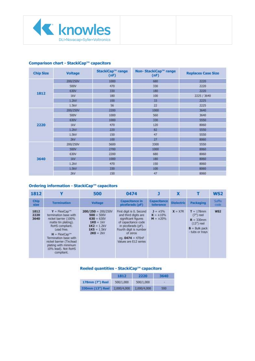
Application Note
Reference No: AN0039
StackiCap™ Issue 4
Page 7 of 7
Range and Ordering Information

AN0040 Issue 4 - Residual Capacitance Range
CN# P109825
Residual Capacitance Range
VC1 Suffix
Ranges and Ordering Information ...............................................................4
Complementary Ranges ............................................................................5
Knowles (UK) Limited,
Old Stoke Road, Arminghall, Norwich,
Norfolk, NR14 8SQ, United Kingdom
Tel: +44 (0) 1603 723300
Tel. (Sales): 01603 723310
Fax: +44 (0) 1603 723301
www.knowlescapacitors.com/syfer
Application Note
Reference No: AN0040
Residual Capacitance
Range Issue 4
Page 2 of 5
Introduction
MLCCs are split into 2 main groups, stable Class 2 which includes X7R, X5R and X8R dielectrics and
ultra-stable Class 1 which includes C0G/NP0 dielectrics. Class 3 dielectrics types do exist but are rarely
used. The common and useful factor of these dielectric types is that they have defined performance
characteristics which enable the circuit designer to anticipate the performance under a given set of
conditions.
EIA Code Temperature Range Capacitance Variation
ε
r
Tanδ
Class
C0G
-55°C to +125°C
30ppm/°C
10 – 100
<0.0015
1
X8R
-55°C to +150°C
±15%
~2000
<0.025
2
X7R
-55°C to +125°C
±15%
2000 – 4000
<0.025
2
X5R
-55°C to +85°C
±15%
2000 – 4000
<0.025
2
Y5V
-30°C to +85°C
+22% to -82%
~16000
<0.09
2
Z5U
+10°C to +85°C
+22% to -56%
~8000
<0.04
2
Red text indicate Syfer standard products
Generally speaking the more stable the dielectric the lower the available capacitance value, there is
often a trade-off to be made with the most stable, lowest loss, zero ageing Class 1 materials only
producing low capacitance values. In order to have parts with higher capacitance values Class 2
dielectrics are used, however these are less stable, as can be seen in the table above, and also have
ageing effects and are more lossy.
Another property of Class 2 dielectrics that is rarely mentioned or defined is the Voltage Coefficient of
Capacitance or VCC. This can often be very significant and have a serious impact on the performance
of the circuit depending on the application requirements. Some dielectric materials and capacitor
ranges are available which have improved VCC performance but these can be limited in their scope.
Syfer’s Residual Capacitance range aims to provide a broader range of options in this field.
Technical Information
Developments in materials and processing technology and increased understanding of capacitor design
and failure modes over time has led to vast improvements in multilayer ceramic capacitor volumetric
efficiency. For instance 10 years ago Syfer could offer an 1812 1kV 56nF, today that has increased to
180nF. An increase of 3 times seems, and is, significant but developments in BME and tape technology
in low voltage components have far exceeded this statistic. The trade off is that, in some cases the
actual capacitance remaining, the “residual capacitance” can be dramatically reduced by the conditions
in which the capacitor operates.
VCC is related to the dielectric material and the voltage stress applied to said dielectric material.
Increasing the dielectric strength of the material, by modification or improved quality, allows for a
reduction in dielectric thickness which is where the large gains in volumetric efficiency are made. A
halving of dielectric thickness can allow for a fourfold increase in available capacitance value as there
can be twice the number of layers in a given thickness and they are half the distance apart,
capacitance being proportional to total overlap area divided by plate separation.
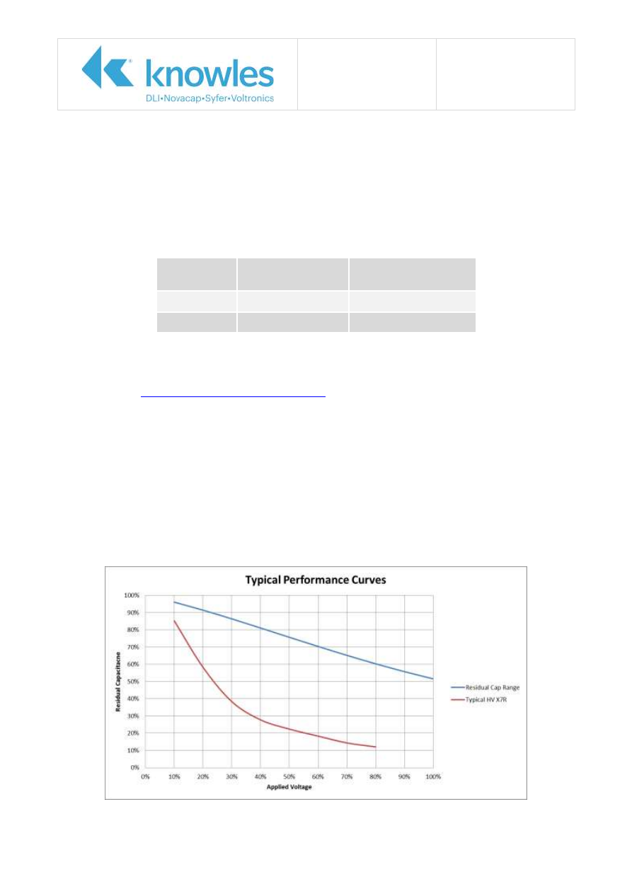
Application Note
Reference No: AN0040
Residual Capacitance
Range Issue 4
Page 3 of 5
This striving for reduction of dielectric thickness has resulted in a continuous worsening of VCC
performance; it is not unheard of for capacitors to lose over 90% of their nominal capacitance value at
rated voltage. Typically higher voltage components will perform worse than lower voltage due to
relative processing safety margins. Despite this drawback these parts do deliver more capacitance and
with many users derating from rated voltage the effect can be manageable. In some cases, where
stability is more important, parts can be designed with this in mind as the VCC is fairly predictable.
There are dielectric designations which address this requirement for stability, the MIL standard BZ and
BX or IECQ-CECC 2C1 and 2X1 classifications are 2 examples:
Classification
Temperature
Range
Capacitance Variation
with Rated DC
2C1/BZ
-55°C to +125°C
+20%/-30%
2X1/BX
-55°C to +125°C
+15%/-25%
These parts do provide excellent stability but this comes at a cost, the ranges are extremely restricted
in their scope as a result of the effective derating required to hold the VCC to the required level,
Syfer’s offering extends to 200V 2225 case size and 120nF in the 2C1(BZ) type. See 2C1(BZ) and
2X1(BX) ranges at
www.knowlescapacitors.com/syfer
and at the end of this document.
There is a need to provide a balance between the headline capacitance values available in standard
X7R and the the outright stability of MIL type dielectrics, there is also a requirement to offer improved
voltage stability in larger case sizes and higher voltages, Syfer have evaluated the characteristics of
our dielectric materials and fixed designs to provide reliable and consistent performance.
The Syfer residual capacitance range MLCCs are intended to provide a more stable capacitance value
with voltage. They are designed so that, at room temperature, the capacitance should not drop below
50% of the 1Vrms 1kHz value all the way up to full rated DC voltage. The parts can be operated
continuously at full rated voltage but if derated will maintain a larger percentage of their original
capacitance value, if operated at 80% of rated voltage the capaciance drop will be approximately 40%.
See graph below for capacitance variation with voltage:

Application Note
Reference No: AN0040
Residual Capacitance
Range Issue 4
Page 4 of 5
Ranges and Ordering Information
This defined range is available and can be ordered by appending the suffix code VC1 to the standard
Syfer part number within the range below. Syfer also has the data to provide bespoke parts with
defined VCC behaviour. We have previously manufactured parts with defined characteristics up to 10kV
DC. For additional queries and requirements
please contact our Sales Department on:
+44 1603 723310 or by Email at
Residual Capacitance Range VC1 Suffix
Voltage
0805
1206
1210
1812
2220
2225
3640
250
12nF
39nF
82nF
220nF
680nF
1uF
1.8uF
500
2.2nF
6.8nF
15nF
56nF
150nF
220nF
560nF
630
1.5nF
4.7nF
8.2nF
39nF
100nF
120nF
470nF
1000
390pF
1.5nF
2.7nF
15nF
39nF
56nF
180nF
1200
-
1nF
2.2nF
10nF
27nF
39nF
120nF
1500
-
560pF
1.2nF
5.6nF
15nF
22nF
68nF
2000
-
270pF
560pF
3.3nF
10nF
12nF
39nF
2500
-
-
-
1.8nF
5.6nF
8.2nF
22nF
3000
-
-
-
-
3.9nF
5.6nF
12nF
Ordering Information Example:
Case Size Termination
Voltage
Capacitance Tolerance
Dielectric
Packaging
Suffix
1206
Y
1K0
0152
K
X
T
VC1
Part number: 1206
Y
1K00152K
X
T
VC1 – Red characters are fixed.
Application Note
Reference No: AN0040
Residual Capacitance
Range Issue 4
Page 5 of 5
Complementary Ranges
2C1 (BZ)
Voltage
0603
0805
1206
1210
1808
1812
2220
2225
50
5.6nF 33nF
120nF 220nF
220nF
470nF
1.2µF*
1.5µF
100
1.5nF 12nF
39nF* 82nF*
100nF*
180nF
470nF*
560nF*
200
-
2.7nF 8.2nF
22nF*
22nF*
56nF*
82nF*
120nF
*Indicates that some values are not RoHS compliant, see
www.knowlescapacitors.com/syfer
2X1 (BX)
Voltage
0603
0805
1206
1210
1808
1812
2220
2225
50
4.7nF* 22nF
68nF
150nF 180nF*
390nF
820nF
1.0µF
100
1.2nF* 8.2nF
22nF
68nF*
68nF*
150nF* 330nF* 470nF*
200
-
1.5nF 5.6nF* 18nF*
18nF*
47nF*
82nF*
100nF*
*Indicates that some values are not RoHS compliant, see
www.knowlescapacitors.com/syfer

AN0042 Issue 2 – PSL range with FlexiCap™ Termination
CN# P109825
PSL Range with
Termination
“The PSL range already provides a high quality component suitable for
demanding applications such as power supplies, DC-DC converters and LED
lighting. Thus with the addition of a termination material specifically
designed to absorb greater levels of mechanical stress and the reduction of
capacitor failures associated with mechanical cracking, the PSL range is
enhanced”.
Introduction ..................................................................... 2
.................................................................................... 4
Test Summary .......................................................................... 6
Knowles (UK) Limited,
Old Stoke Road, Arminghall, Norwich,
Norfolk, NR14 8SQ, United Kingdom
Tel: +44 (0) 1603 723300
Tel. (Sales): 01603 723310
Fax: +44 (0) 1603 723301
www.knowlescapacitors.com/syfer
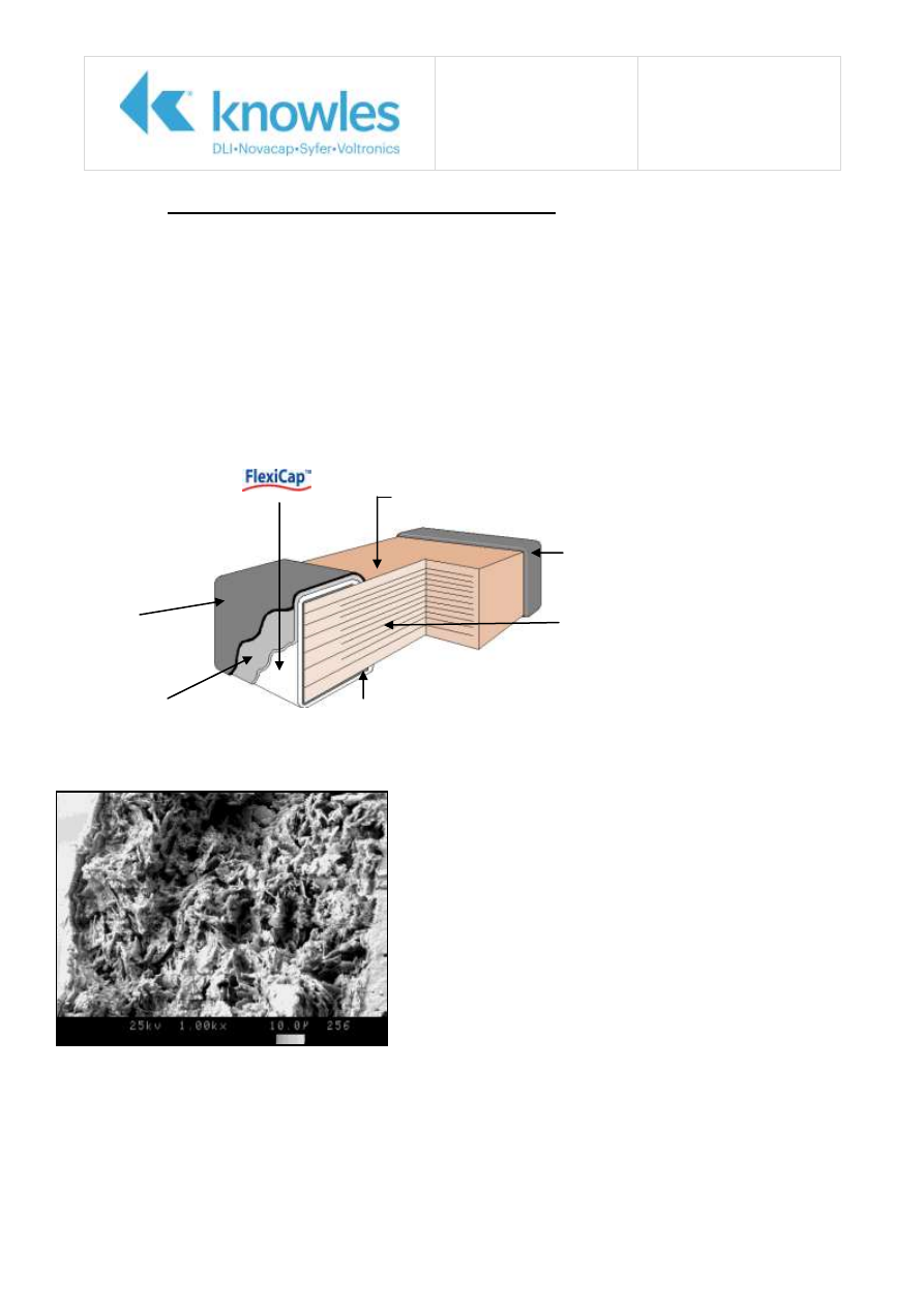
Application Note
Reference No.
AN0042 – PSL range
with FlexiCap™
Issue 2
Page 2 of 9
PSL range with
FlexiCap
™
Introduction
Syfer Technology Ltd introduced FlexiCap
™
in 1999 and became the first multilayer capacitor
manufacturer to offer a flexible termination to customers. This type of termination has proven to be
very successful as customers realize the benefits and also as demonstrated by other capacitor
manufacturers subsequently introducing flexible terminations, some with very similar names to
FlexiCap
™
.
The PSL range with FlexiCap
™
refers to a flexible termination material that is applied over a sintered
termination. The FlexiCap
™
material is a silver loaded epoxy polymer that is applied using conventional
termination techniques and then cured at 180ºC. Following the curing process, components are
processed through the same manufacturing, test and inspection stages when compared with a
standard PSL component.
Termination
Material
Metal
Electrodes
Picture taken at 1000x
magnification using a SEM showing
a fracture section through a
capacitor termination.
The picture demonstrates the
fibrous nature of the FlexiCap
™
termination that absorbs greater
levels of mechanical stress when
compared with standard sintered
termination.
Fig 1. Capacitor Construction
Tin
Outer Layer
Intermediate
Nickel Layer
Fired Ceramic
Dielectric
Sintered
Base Layer

Application Note
Reference No.
AN0042 – PSL range
with FlexiCap™
Issue 2
Page 3 of 9
Queens Award for Innovation
The Queen's Awards for Enterprise are the UK's most prestigious awards for business performance. The
Awards are presented in three categories: International Trade, Innovation and Sustainable
Development
The Awards are made each year by The Queen, on the advice of the Prime Minister, who is assisted by
an Advisory Committee that includes representatives of UK Government, industry and commerce, and
the trade unions.
The Queens Award for Innovation recognizes companies that have demonstrated commercial success
through innovative products or services.
Her Majesty The Queen conferred the Queens Award for Innovation upon Syfer Technology Ltd in 2008
for recognition of outstanding achievements in Innovation with respect to FlexiCap
™
.
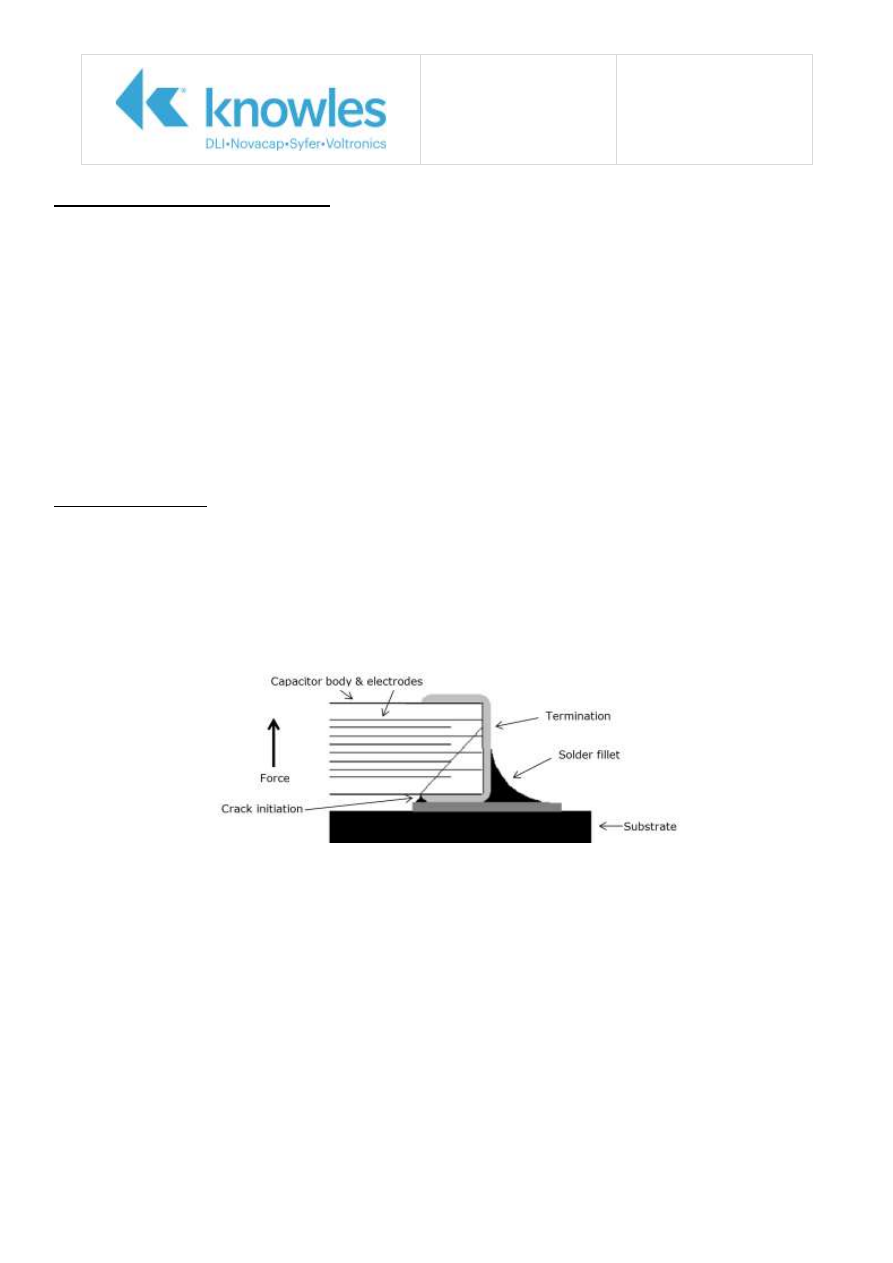
Application Note
Reference No.
AN0042 – PSL range
with FlexiCap™
Issue 2
Page 4 of 9
Benefits of Using FlexiCap
™
Sintered termination materials are fired onto the ceramic body of the component at approximately
800ºC. The result is a very hard material that provides minimal protection to the ceramic body of the
component with respect to mechanical strain when the component is situated on an assembly.
FlexiCap
™
termination material is a silver loaded epoxy polymer that is flexible and absorbs some of
the mechanical strain between the PCB and the ceramic component. Components terminated with
FlexiCap
™
withstand greater levels of mechanical strain when compared with sintered terminated
components alone.
Types of mechanical strain where FlexiCap
™
terminated capacitors offer enhanced protection include
mechanical cracking (which is the largest cause for ceramic component failure) and also in applications
where rapid temperature changes can occur. The PSL range is manufactured to exacting standards
using our unique screen printing process. This provides a high quality component suitable for
demanding applications and is suitable for extreme environments
Mechanical Cracking
Due to its brittle nature, multilayer ceramic capacitors are more prone to excesses of mechanical stress
than other components used in surface mounting. One of the most common causes of capacitor
failures is directly attributable to bending of the printed circuit board (PCB) after solder attachment.
Excessive bending will create mechanical crack(s) within the ceramic capacitor. Mechanical cracks,
depending upon severity, may not cause capacitor failure during the final assembly test. Over time
moisture penetration into the crack can cause a reduction in insulation resistance and eventual
dielectric breakdown leading to capacitor failure in service.
Fig 1. Mechanical Crack
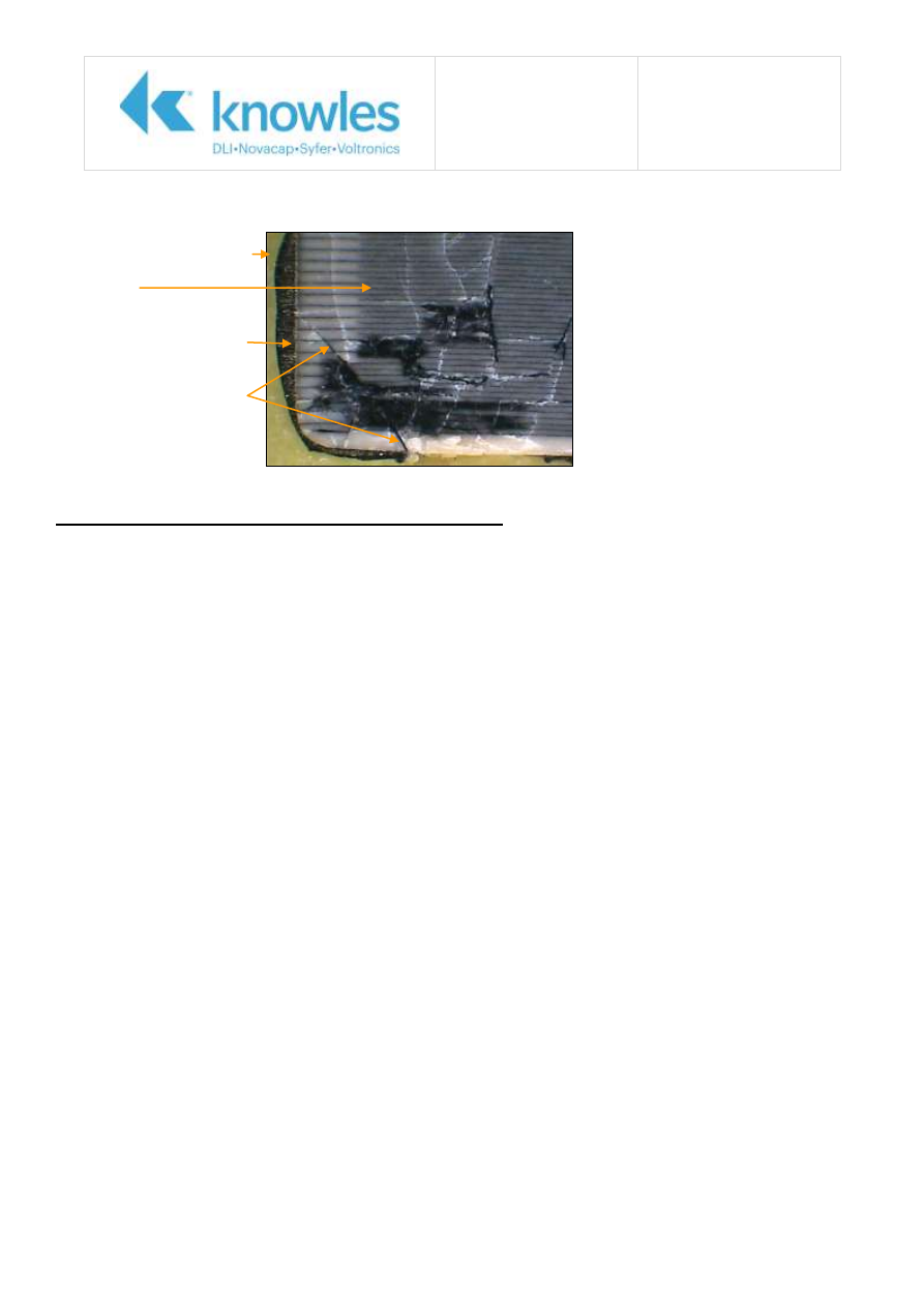
Application Note
Reference No.
AN0042 – PSL range
with FlexiCap™
Issue 2
Page 5 of 9
Example of a capacitor issued by a customer to Syfer for failure investigation:
Customer Assembly Process Requirements
Capacitors with FlexiCap
™
termination should be handled, stored and transported in the same manner
as capacitors with only sintered termination. The requirements for mounting and soldering capacitors
with FlexiCap
™
termination are the same as for capacitors with only sintered termination.
Components with FlexiCap
™
are compatible with lead solder applications and lead-free solder
applications with a maximum recommended reflow temperature of 270ºC.
PSL with FlexiCap
™
Moisture Sensitivity Level (MSL) = 1.
Yellow potting compound
Electrodes
Standard termination
material (not FlexiCap
™
)
Mechanical crack (caused
capacitor failure)
Black areas are
damaged sections
within the capacitor
caused during the
electrical failure
White lines are
thermal cracks
created during the
electrical failure
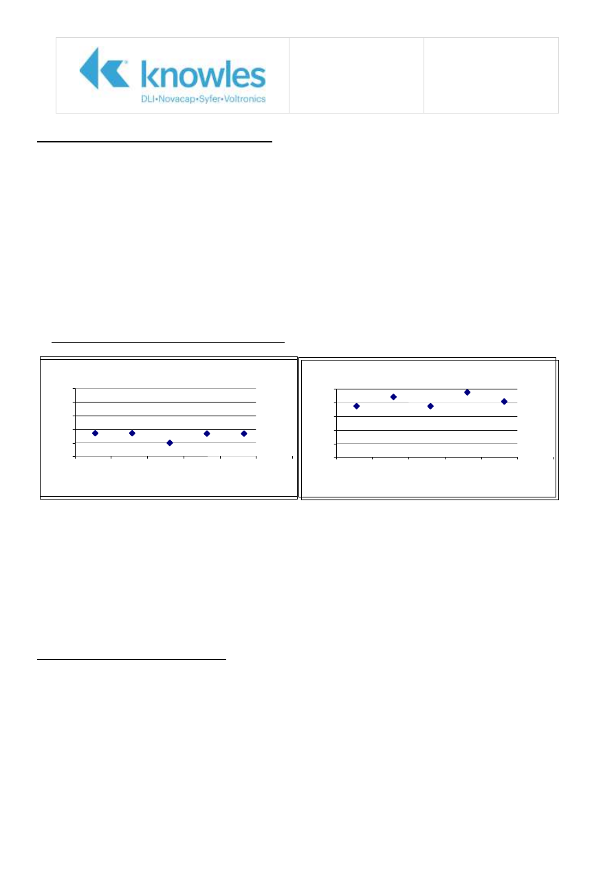
Application Note
Reference No.
AN0042 – PSL range
with FlexiCap™
Issue 2
Page 6 of 9
PSL with FlexiCap
™
Test Summary
PSL with FlexiCap
™
has been rigorously tested and approved/ qualified to the following test
requirements:
Syfer qualification and ongoing routine tests.
AEC-Q200 qualification.
The key tests with respect to PSL with FlexiCap
™
performance are as follows.
Bend Test (Board Flex).
Method: Capacitor samples mounted onto a 100mm FR4 Test PCB and subjected to bend testing
in accordance with IEC 60068-2-21. Environmental testing: Test U: Robustness of
terminations and integral mounting devices or AEC-Q200-005.
(10mm maximum bend test equipment capability)
PSL performance with and without FlexiCap
™
The bend test summary provides a comparison between component case sizes in the following
groups:
PSL X7R dielectric material without FlexiCap
™
termination material.
PSL X7R dielectric material with FlexiCap
™
termination material.
The bend tests conducted confirm that with FlexiCap
™
termination the PSL component withstands
greater mechanical strain.
Temperature Cycling.
Background on Temperature Cycling
Rapid temperature changes when components are mounted on a PCB can induce stress as a result of
different material CTE (Coefficient of Thermal Expansion) rates. For example, a sintered terminated
component will typically fail a temperature cycle test consisting of 1000 cycles (-55ºC to 125ºC). The
difference in material (PCB, ceramic, solder) expansion rates can induce cracks within components that
cause components to electrically fail.
The FlexiCap
™
termination material absorbs some of the strain created during repeated rapid
temperature changes and PSL components terminated with FlexiCap
™
pass temperature cycle tests
such as 1000 cycles (-55ºC to 125ºC). Reference JESD22-A104.
Mean Bend -
Termination (Y) code
0
2
4
6
8
10
X7R
0805 Y
X7R
1206 Y
X7R
1210 Y
X7R
1812 Y
X7R
2220 Y
Case Size
mm
PSL with FlexiCap
™
Mean Bend -
Termination (J) code
0
2
4
6
8
10
X7R
0805 J
X7R
1206 J
X7R
1210 J
X7R
1812 J
X7R
2220 J
mm
PSL without FlexiCap
™
Case Size
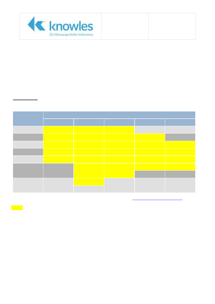
Application Note
Reference No.
AN0042 – PSL range
with FlexiCap™
Issue 2
Page 7 of 9
Customer Qualification
The FlexiCap
™
termination material has used been customers since 1999 and the qualifications
conducted by customers have been successful. The reaction to FlexiCap
™
termination has been
extremely favourable and the demand for FlexiCap
™
terminated capacitors continues to increase as
customers realize the advantages provided.
FlexiCap
™
terminated capacitors are supplied to many blue chip companies, O.E.M’s, E.M.S’s and
international component distributors. Applications include telecoms, military, aerospace, automotive,
industrial and power supplies.
PSL range
Minimum/maximum capacitance values - PSL capacitors
Rated Voltage
Chip Size
0805
1206
1210
1812
2220
50V/63V
220pF - 100nF
470pF - 470nF
1nF - 1µF
N/A
N/A
100V
220pF - 47nF
470pF - 150nF
1nF - 330nF
1nF - 680nF
1nF – 1.5µF
200V/250V
220pF - 27nF
470pF - 100nF
1nF - 180nF
1nF - 470nF
1nF – 1µF
500V
220pF - 10nF
470pF - 56nF
1nF - 100nF
1nF - 220nF
1nF - 560nF
630V
220pF - 5.6nF
470pF - 47nF
1nF - 68nF
1nF - 150nF
1nF - 330nF
1000V
220pF - 3.3nF
470pF - 10nF
1nF - 22nF
1nF - 68nF
1nF - 100nF
1nF - 330nF
1nF - 120nF
2000V
N/A
470pF – 1nF
1nF - 4.7nF
1nF - 10nF
N/A
470pF - 2.2nF
Note:
Other capacitance values may become available, please contact our Sales Office if you need values other than those
shown in the above table. For dimensions and soldering information, please visit
www.knowlescapacitors.com/syfer
= AECQ200
Application Note
Reference No.
AN0042 – PSL range
with FlexiCap™
Issue 2
Page 8 of 9
Ordering information - PSL capacitors
1206
Y
1K0
0103
K
J
T
Chip size
Termination
Voltage
Capacitance in Pico farads
(pF)
Capacitance
tolerance
Dielectric
Packaging
0805
J
= Nickel barrier with 100% matte tin
plating. RoHS compliant.
Y
=FlexiCap™ termination base with nickel
barrier (100% matte tin plating). RoHS
compliant. Lead free.
050
= 50V
First digit is 0.
Second and third digits are
significant figures of
capacitance code.
The fourth digit is number of
0’s following.
Example:
0103
= 10000pF
K
= ±10%
J
= X7R
T
= 178mm
1206
063
= 63V
M
= ±20%
S
= X7R
AEC-Q200
(7”) reel
1210
100
= 100V
R
= 330mm
1812
200
= 200V
(13”) reel
2220
250
= 250V
B
= Bulk
500
= 500V
pack - tubs
630
= 630V
1K0
= 1kV
2K0
= 2kV
Reeled quantities - PSL capacitors
Chip Size
0805
1206
1210
1812
2220
7” Reel
3,000
2,500
2,000
500/1,000*
500/1,000*
13” Reel
12,000
10,000
8,000
2,000/4,000*
2,000/4,000*
*
Reel quantity depends on chip thickness. Please contact our sales office.
Application Note
Reference No.
AN0042 – PSL range
with FlexiCap™
Issue 2
Page 9 of 9
Additional Information
Syfer has generated a comprehensive range of application notes (available at
www.knowlescapacitors.com/syfer/en/gn/technical-info/application-notes
) to provide additional
information to customers.
Application notes that provide additional information with respect to FlexiCap
™
:
APPLICATION NOTE
CONTENTS
AN0001
FlexCap
TM
Termination
AN0002 Bend Testing
Test methods for Capacitor bend testing, and the
shape of typical cracks
AN0005 Mechanical Cracking
Potential causes of mechanical cracking, corrective
actions and depanelisation methods
AN0006 Dielectric Ageing
Capacitor dielectric ageing
AN0009 AEC-Q200 Stress Test Qualification
Provides information on tests performed by Syfer in
accordance with the AEC-Q200 specification
AN0010 Lead-free soldering and bend test
performance
The effects of Lead-free soldering on bend testing
through solder choice
AN0019 Tin Whiskers
Tin Whiskers mitigation and surface mount chip
capacitors
AN0021 Tandem Capacitors
Tandem capacitors terminated with FlexiCap™
provide an ultra-robust and reliable component.
AN0022 Open Mode Capacitors
Open mode capacitors terminated with FlexiCap™
provide a robust component that fail in an open
circuit mode.
AN0024 Moisture Sensitivity Level Classification
for Syfer products
MSL classification IPC / JEDEC J-STD-020D for Syfer
products.
AN0026 Outgassing test results for FlexiCap™
capacitors
Results for ECSS-Q-70-02A outgassing tests on
FlexiCap™ capacitors.
AN0028 Soldering / Mounting Chip Capacitors,
Radial Leaded Capacitors and EMI Filters
This gives guidance to engineers and board designers
on mounting and soldering Syfer products.