Sales and Corporate Office
1717 Chicago Avenue
Riverside, California 92507-2364
Phone: (951) 788-1700
Fax: (951) 369-1151
Applications Engineering
17271 North Umpqua Hwy.
Roseburg, Oregon 97470-9422
Phone: (541) 496-0700
Fax: (541) 496-0408
e-mail: caddock@caddock.com • web: www.caddock.com
For Caddock Distributors listed by country see caddock.com/contact/dist.html
© 2004 Caddock Electronics, Inc.
CAD
K
DOC
CC1512FC Standard Resistance Values:
Tolerance CC1512FC ±1% Standard (except as noted).
CC2015FC Standard Resistance Values:
Tolerance CC2015FC ±1% Standard (except as noted).
CC2520FC Standard Resistance Values:
0.010
Ω
5%
0.015
Ω
5%
0.020
Ω
5%
0.025
Ω
5%
0.030
Ω
5%
Tolerance CC2520FC ±1% Standard (except as noted).
0.033
Ω
5%
0.040
Ω
5%
0.050
Ω
2%
0.075
Ω
2%
0.10
Ω
0.15
Ω
0.20
Ω
0.25
Ω
0.30
Ω
0.33
Ω
0.40
Ω
0.50
Ω
0.75
Ω
1.00
Ω
1.50
Ω
2.00
Ω
2.50
Ω
3.00
Ω
0.010
Ω
5%
0.015
Ω
5%
0.020
Ω
5%
0.025
Ω
5%
0.030
Ω
5%
0.033
Ω
5%
0.040
Ω
5%
0.050
Ω
2%
0.075
Ω
2%
0.10
Ω
0.15
Ω
0.20
Ω
0.25
Ω
0.30
Ω
0.33
Ω
0.40
Ω
0.50
Ω
0.75
Ω
1.00
Ω
1.50
Ω
2.00
Ω
2.50
Ω
3.00
Ω
0.020
Ω
5%
0.025
Ω
5%
0.030
Ω
5%
0.033
Ω
5%
0.040
Ω
5%
0.050
Ω
2%
0.075
Ω
2%
0.10
Ω
0.15
Ω
0.20
Ω
0.25
Ω
0.30
Ω
0.33
Ω
0.40
Ω
0.50
Ω
0.75
Ω
1.00
Ω
1.50
Ω
2.00
Ω
2.50
Ω
3.00
Ω
3.30
Ω
4.00
Ω
5.00
Ω
7.50
Ω
8.00
Ω
10.0
Ω
Custom resistance values and non-standard tolerances
can be manufactured for high quantity applications.
Please contact Caddock Applications Engineering.
Recommended Circuit Board Layout
(current and sense connections):
Fig. 1A:
Kelvin layout recom-
mended for values below 0.20
Ω
Fig. 1B:
Kelvin layout
recommended for higher
resistance values.
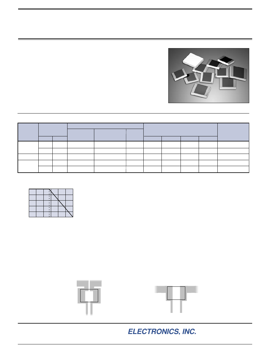
Type CC Low Resistance Precision Chip Resistors
Style FC - Flip Chip Version
is a surface mount version with solderable pads for
flip chip
soldering.
Note 1: General Applications -
The power rating
for general applications is based upon 0.5 sq. in.
(300 mm
2
) of termination pad or trace area (2 oz.
copper) connected to each end of the resistor.
Maximum chip temperature is 150°C. Use Derating
Curve to derate appropriately for the maximum
ambient temperature and for the temperature
limitations of the adjacent materials.
Note 2: Thermal Resistance -
In High Power Applications where the circuit board
material provides high heat sinking benefits (such as IMS, Alumina, or other) the thermal
resistance of the chip resistor is useful to establish the maximum power capability of the
chip resistor in the application. The film temperature is measured at the center of the
resistor element and the solder pad temperature is measured at the center of the
termination pad (point X in the recommended circuit layouts shown below). Maximum
temperature of the chip resistor (at the center of chip) should not exceed 150°C through
the temperature range of the application
.
Style FC Derating Curve For General Applications
3.30
Ω
4.00
Ω
5.00
Ω
7.50
Ω
8.00
Ω
10.0
Ω
3.30
Ω
4.00
Ω
5.00
Ω
7.50
Ω
8.00
Ω
10.0
Ω
S S
X
X
C
C
C
X
X
S
S
C
C
C = Current connection
S = Sense connection
Note: Actual width of current trace is based on magnitude of current. Point of connection should be in the area shown.
0.015
Ω
0.010
Ω
Model
Resistance
Min.
Max.
Power Capability Information
CC1512FC
CC2015FC
CC2520FC
10.0
Ω
0.020
Ω
10.0
Ω
0.020
Ω
10.0
Ω
0.020
Ω
0.010
Ω
0.025
Ω
150
°
C
0.75 Watt
Max. Chip
Temperature
General Applications High Power Applications
Thermal Resistance -
R
θ
JC
Film (J) to Solder Pad (C)
(see note 2)
22.7
°
C/Watt
Power Rating
at 70
°
C
(see note 1)
22.7
°
C/Watt
16.0
°
C/Watt
13.0
°
C/Watt
11.5
°
C/Watt
150
°
C
150
°
C
150
°
C
150
°
C
Dimensions in inches and (millimeters)
.150
±
.007
(3.81
±
.18)
A
B
D
.120
±
.007
(3.05
±
.18)
.035 min.
(0.89 min.)
C
.027
±
.005
(.69
±
.13)
.250
±
.007
(6.35
±
.18)
.200
±
.007
(5.08
±
.18)
.065 min.
(1.66 min.)
.032
±
.005
(.81
±
.13)
.250
±
.007
(6.35
±
.18)
.200
±
.007
(5.08
±
.18)
.040 min.
(1.02 min.)
.041
±
.004
(1.04
±
.10)
.200
±
.007
(5.08
±
.18)
.150
±
.007
(3.81
±
.18)
.050 min.
(1.27 min.)
.027
±
.003
(.69
±
.08)
.150
±
.007
(3.81
±
.18)
.120
±
.007
(3.05
±
.18)
.035 min.
(0.89 min.)
.022
±
.003
(.56
±
.08)
Comments
Solder Coated Pads
Solderable Pads
Solderable Pads
Solder Coated Pads
Solderable Pads
0.75 Watt
1.0 Watt
1.5 Watts
1.5 Watts
AMBIENT TEMPERATURE, C
RA
TED LOAD, %
o
100
80
60
40
20
0
25
100
150
70
•
Style FC
- Flip Chip version for surface mount applications.
Style WB
- Wire Bond version for hybrid applications with metallized back
surface for solder down heat sinking of the chip, includes bondable termination
pads to receive aluminum wire bonds.
• Thermal resistance is provided to optimize high power designs when utilizing
higher thermal conductivity circuit board substrates such as IMS or Alumina.
• Resistance range down to 0.010 ohm at ±5%, 0.050 ohm at ±2%,
and 0.10 ohm at ±1%.
• Low inductance provides excellent high frequency and pulse response.
• High pulse handling and overload capability.
• Best choice for switching power supplies, motor speed controls, and high
current sensing applications.
Page 1 of 2
28_IL106.1004