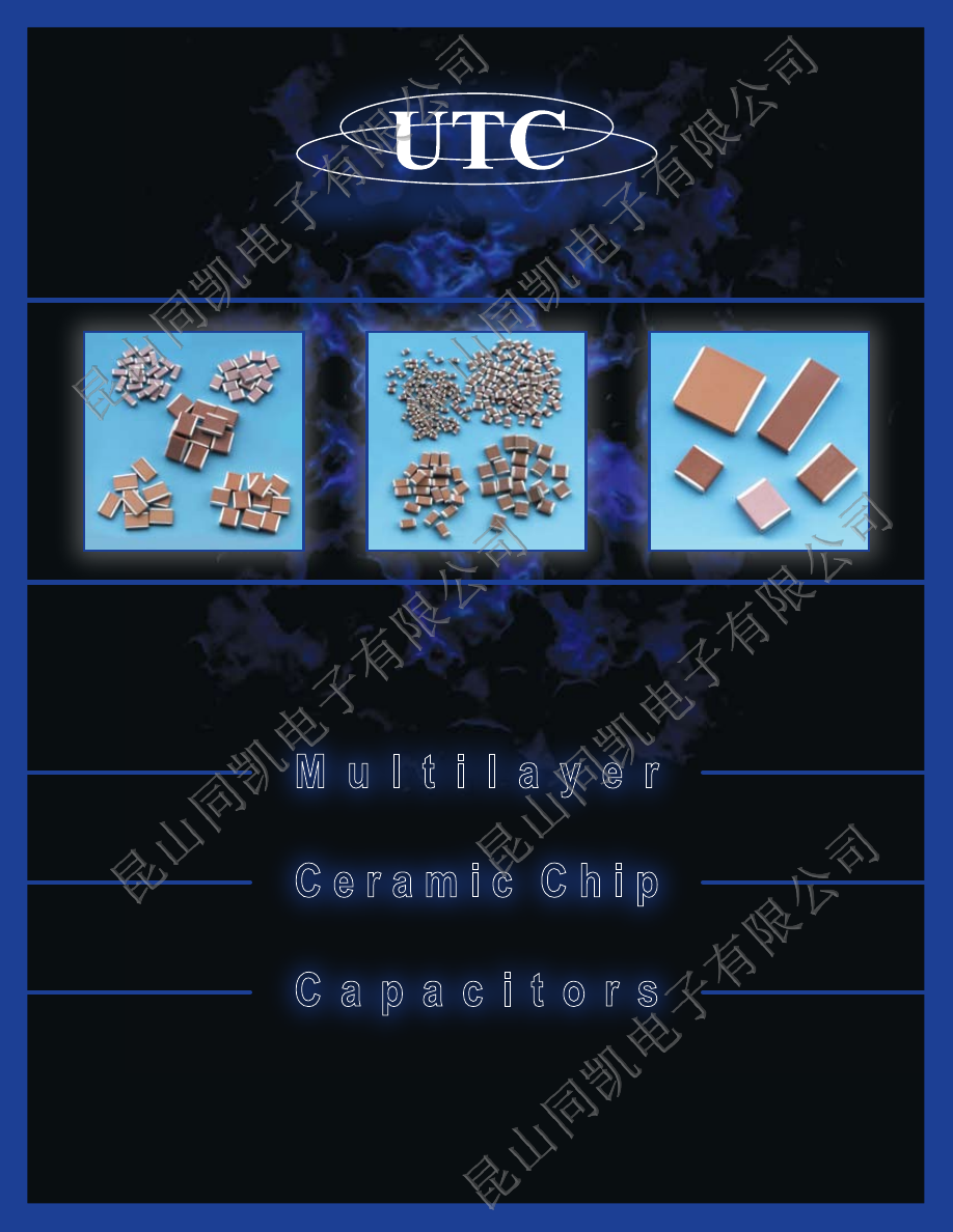
UNION TECHNOLOGY CORP.
M u l t i l a y e r
C e r a m i c C h i p
C a p a c i t o r s
UNION TECHNOLOGY CORP.
M u l t i l a y e r
C e r a m i c C h i p
C a p a c i t o r s
OVERVIEW
Union Technology Corp. (UTC) is a global provider for the design and manufacture of multilayer ceramic capacitors
for use in: commercial, industrial and high reliability applications.
Product offering:
• SMT multilayer ceramic chips
• Radial Leaded High Voltage Capacitors
• SMT High Voltage MLCC
• Switch Mode Power Supply Capacitors (SMPS)
• SMT Large Body Size MLCC
• Planar Arrays & Discoidal Capacitors
QUALITY
UTC integrates quality throughout its supply chain system by building quality into our designs and manufacturing
process. Supplier control systems ensure the highest quality materials and service to our customers. Our manufacturing
facility is ISO 9001:2000 certified and MIL-STD-790 approved.
UTC is equipped for performing testing in accordance with MIL-PRF-39014, MIL-PRF-20, and MIL-PRF-55681
as required by some customers. Our quality assurance system and procedures are based upon the requirements of
MIL-I-45208 and MIL-STD-790, with the calibration program in accordance with MIL-STD-45662A.
OPERATIONS
Established in 1991, UTC is a Corporation headquartered in Monterey Park, California. Within this 25,000 square
foot facility, UTC houses its technology center, manufacturing operations along with the sales and customer
support staff. UTC also maintains a fully staffed, highly qualified engineering department to support customer
applications, product design, and new product development.
UTC’s global network of sales representatives and distributors are prepared to assist you with designing our
products to meet your application requirements.
ENVIROMENT
UTC is fully committed to helping the cause of achieving and maintaining a clean environment. The complete
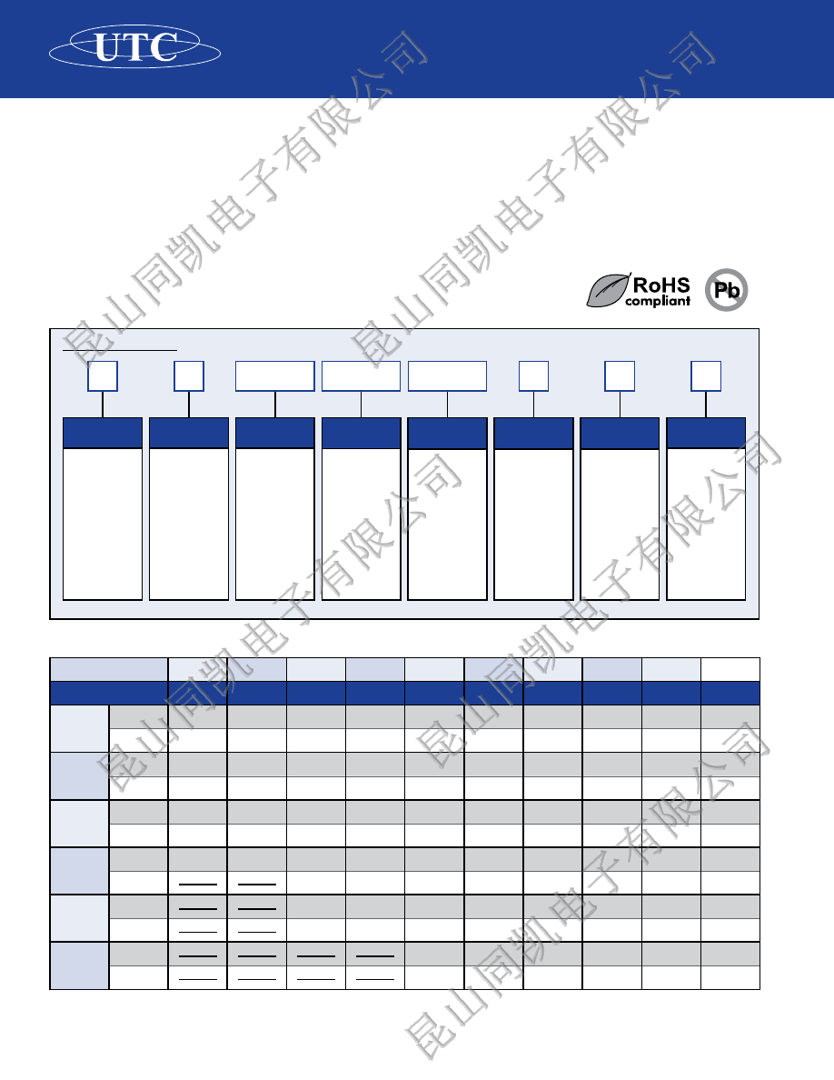
UTC offering of commercial ceramic chips within this catalog are designed and produced to be lead-free and are
fully RoHS compliant.
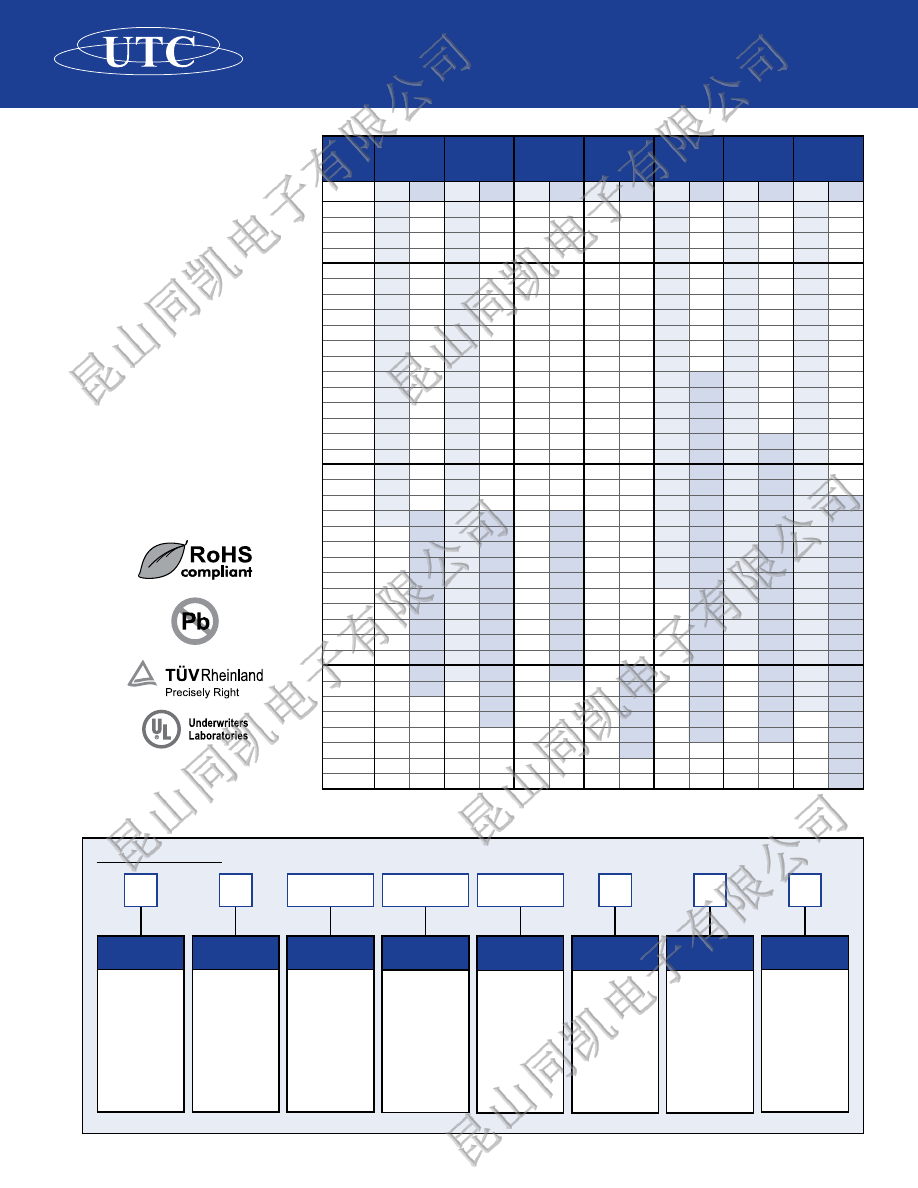
ISO 9001: 2000
C E R T I F I E D
COMPANY OVERVIEW
1
PRODUCT OVERVIEW
Union Technology Corp. is a global supplier of ceramic chip capacitors and other specialty multilayer ceramic
(MLC) products used by electronic manufacturers.
UTC formulates the materials used in the manufacture of its MLCs, including ceramic dielectric powders, electrode
materials, resins, and inks. Precise raw material characterization and tight process control maintains UTC’s quality
reputation as a state-of-the-art manufacturer of ceramic capacitor products.
UTC offers the full range of standard popular EIA sizes from a 0402 up to 2225. They are available in; NPO, X7R,
X5R, and Y5V dielectrics from 6.3 volts up to ratings of 5,000 volts.
In addition to our standard chip products UTC does support many custom application specific designs which
include capacitors that have voltage ratings up to 10 KV and chip sizes as large as 6560. Our Advanced Products
Group is staffed and equipped to assist customers with developing these MLC solutions for their specific
applications requiring cost effective, volumetric efficient designs.
TABLE OF CONTENTS
Company Overview . . . . . . . . . . . . . . . . . . . . . . . . . . . . . . . . . . . . . . . . . . . . . . . . . . . . . . . . . . . . 1
Product Overview . . . . . . . . . . . . . . . . . . . . . . . . . . . . . . . . . . . . . . . . . . . . . . . . . . . . . . . . . . . . . . 2
SMT MULTILAYER CERAMIC CAPACITORS
Packaging Specifications . . . . . . . . . . . . . . . . . . . . . . . . . . . . . . . . . . . . . . . . . . . . . . . . . . . . . . . . 3
NPO Dielectric Chips . . . . . . . . . . . . . . . . . . . . . . . . . . . . . . . . . . . . . . . . . . . . . . . . . . . . . . . . . . . 4
X7R Dielectric Chips . . . . . . . . . . . . . . . . . . . . . . . . . . . . . . . . . . . . . . . . . . . . . . . . . . . . . . . . . . . 7
X5R / Y5V Dielectric Chips . . . . . . . . . . . . . . . . . . . . . . . . . . . . . . . . . . . . . . . . . . . . . . . . . . . . . 10
Safety Certified Chips . . . . . . . . . . . . . . . . . . . . . . . . . . . . . . . . . . . . . . . . . . . . . . . . . . . . . . . . . 12
High Voltage Chips . . . . . . . . . . . . . . . . . . . . . . . . . . . . . . . . . . . . . . . . . . . . . . . . . . . . . . . . . . . . 13
Technical Specifications . . . . . . . . . . . . . . . . . . . . . . . . . . . . . . . . . . . . . . . . . . . . . . . . . . . . . . . . 14
Soldering Profiles . . . . . . . . . . . . . . . . . . . . . . . . . . . . . . . . . . . . . . . . . . . . . . . . . . . . . . . . . . . . . 16
MILITARY & CUSTOM PRODUCTS
Switch Mode Power Supply Capacitors . . . . . . . . . . . . . . . . . . . . . . . . . . . . . . . . . . . . . . . . . . . . 17
High Voltage Radial Capacitors . . . . . . . . . . . . . . . . . . . . . . . . . . . . . . . . . . . . . . . . . . . . . . . . . . 17
Feed-Through Discoidal Capacitors . . . . . . . . . . . . . . . . . . . . . . . . . . . . . . . . . . . . . . . . . . . . . . . 17
Planar Capacitor Arrays . . . . . . . . . . . . . . . . . . . . . . . . . . . . . . . . . . . . . . . . . . . . . . . . . . . . . . . . 17
TABLE OF CONTENTS
2
3
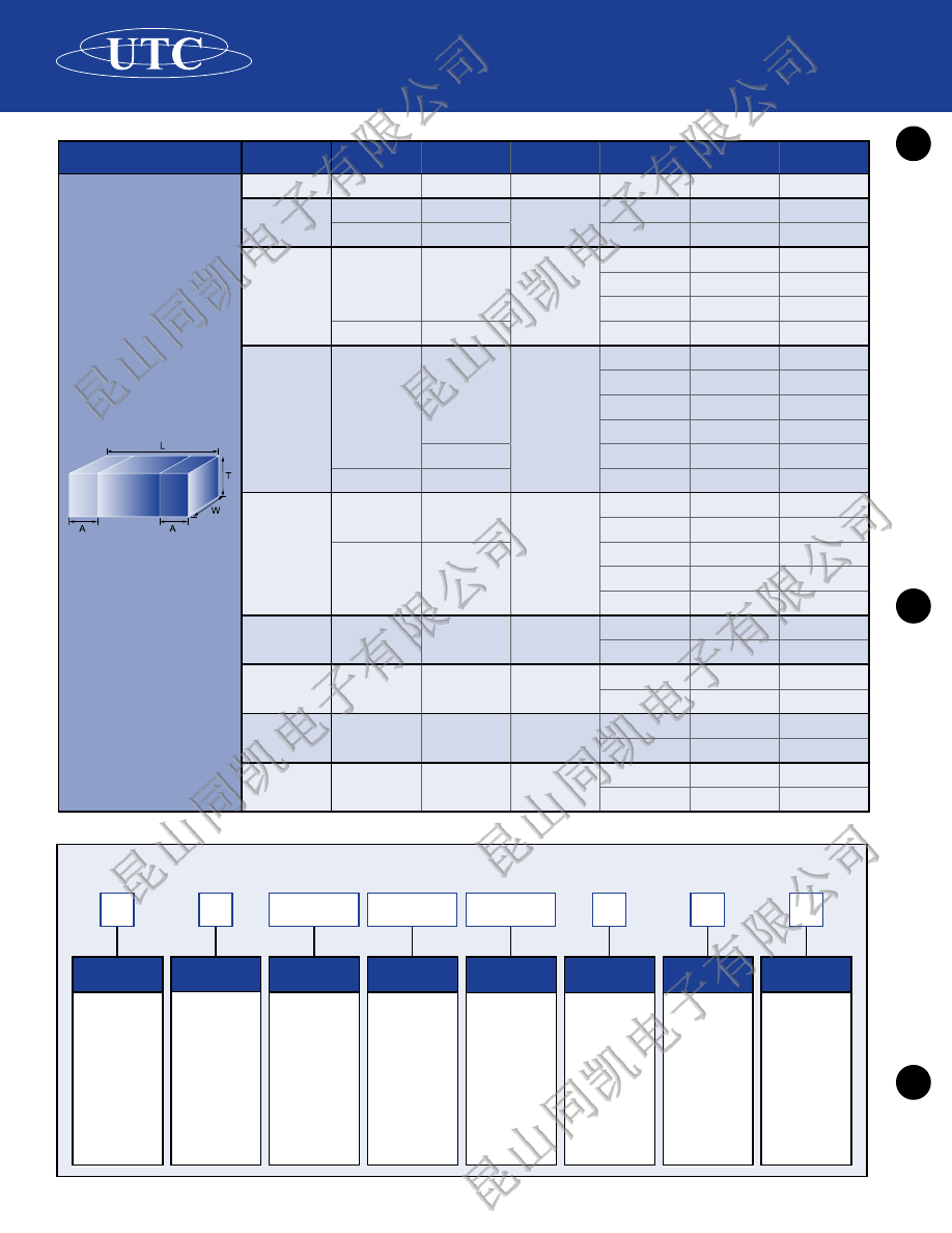
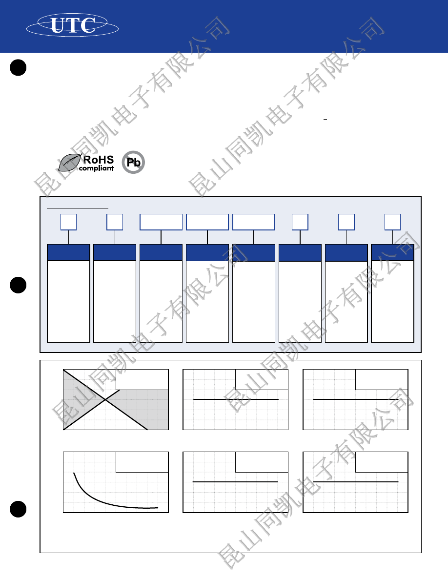
UTC P/N
STYLE
C = MLCC CHIP
S = MLCC SAFETY
CERTIFIED CHIP
C
105
CAPACITANCE
CODE
2 significant
digits are used
plus the third
character then
represents
the number of
zeros to follow
L
VOLTAGE
A = 6.3V
C = 10V
E = 16V
L = 25V
G = 50V
B = 100V
R = 200V
H = 250V
J = 300V
N = 400V
S = 500V
K = 600V
K = 630V
T = 1000V
W = 2000V
X = 3000V
Y = 4000V
Z = 5000V
0805
BODY SIZE
0402
0603
0805
1206
1210
1808
1812
1825
2220
2225
3530
4040
5550
K
TOLERANCE
F = 1%
G = 2%
J = 5%
K = 10%
M = 20%
Z = -20% / +80%
*Cap values < 10pF
B = +/-0.10pF
C = +/-0.25pF
D = +/-0.50pF
W
TERMINATION
W = 100%
tin termination
& RoHS - Lead
Free compliant
product
B = Soft
Termination
[consult factory]
T
PACKAGE
STYLE
T = Tape & Reel
X5R
TEMPERATURE
COEFFICIENT
NPO
X7R
X5R
Y5V
HOW TO ORDER
Outline
Size
Inch (mm)
Length
L (mm)
Width
W (mm)
Termination
A (mm)
Thickness Designation
T (mm)/Symbol
Packaging
Qty/Reel
0402 (1005)
1.00±0.05
0.50±0.05
0.25+0.05/-0.10
N
0.50±0.05
10,000
0603 (1608)
1.60±0.10
0.80±0.10
0.40±0.15
S
0.80±0.07
4,000
1.60+0.15/-0.10
0.80+0.15/-0.10
X
0.80+0.15/-0.10
4,000
0805 (2012)
2.00±0.15
1.25±0.10
0.50±0.20
A
0.60±0.10
4,000
B
0.80±0.10
4,000
D
1.25±0.10
3,000
2.00±0.20
1.25±0.20
I
1.25±0.20
3,000
1206 (3216)
3.20±0.15
1.60±0.15
0.60±0.20
B
0.80±0.10
4,000
C
0.95±0.10
3,000
J
1.15±0.15
3,000
D
1.25±0.10
3,000
1.60±0.20
G
1.60±0.20
2,000
3.20+0.30/-0.10
1.60+0.30/-0.10
P
1.60+0.30/-0.10
2,000
1210 (3225)
3.20±0.30
2.50±0.20
0.75±0.25
C
0.95±0.10
3,000
D
1.25±0.10
3,000
3.20±0.40
2.50±0.30
G
1.60±0.20
2,000
K
2.00±0.20
1,000
M
2.50±0.30
1,000
1808 (4520)
4.50±0.40
2.03±0.25
0.75±0.25
D
1.25±0.10
2,000
K
2.00±0.20
1,000
1812 (4532)
4.50±0.40
3.20±0.30
0.75±0.25*
D
1.25±0.10
1,000
K
2.00±0.20
1,000
2220
5.70±
4.50±
.50±
D
2.50±
1,000
K
2.50±
1,000
2225
5.70±
6.35±
.50±
D
3.05±
1,000
K
3.05±
1,000
MECHANICAL DIMENSIONS &
PACKAGING SPECIFICATIONS
3
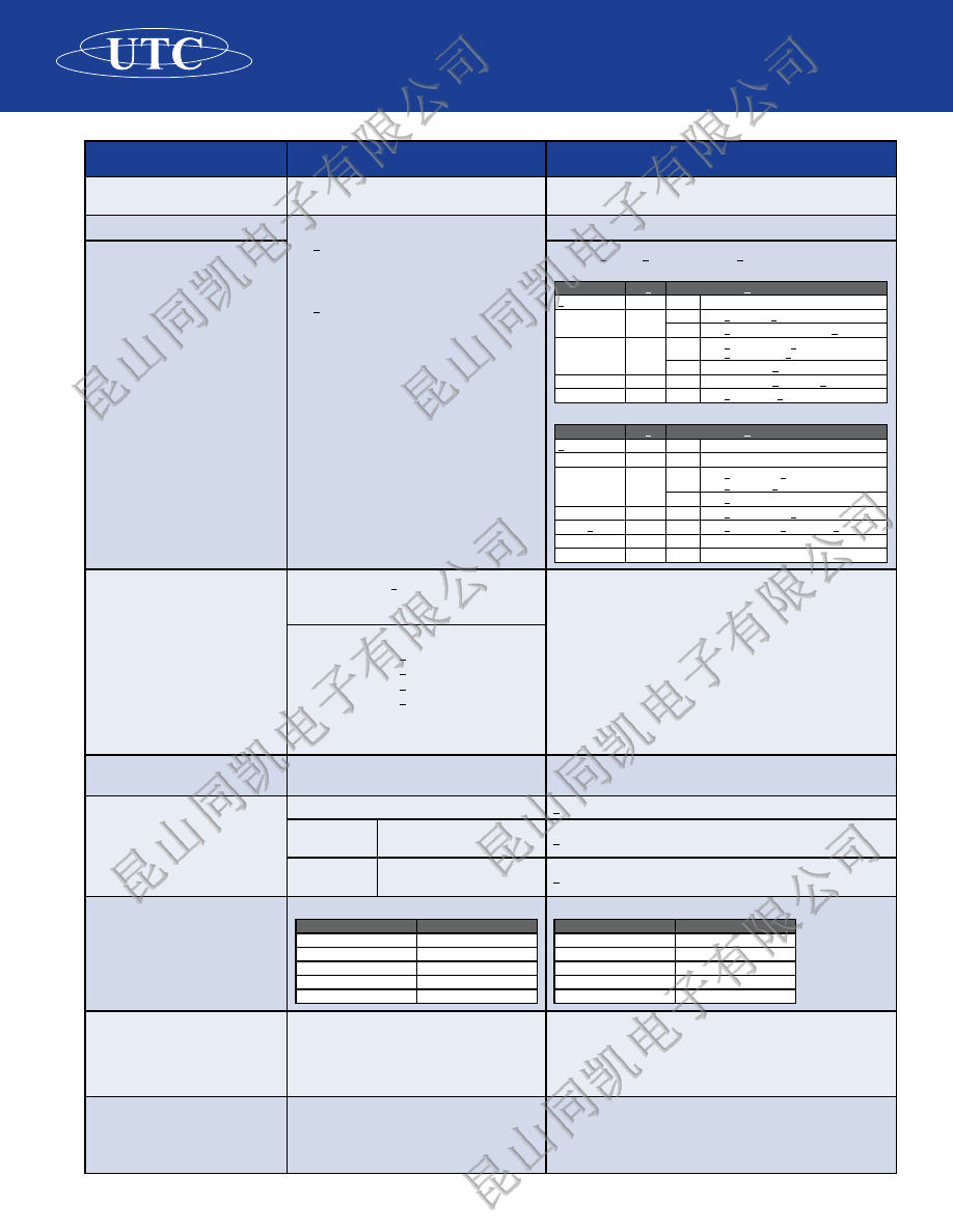
Temperature Coefficient:
< 30 ppm/
o
C, -55
o
C to 125
o
C.
Dissipation Factor:
< 0.1 % @ 1 MHz, 25
o
C.
Insulation Resistance:
1000ΩF or 100GΩ, whichever is less @ rated volt
-
age 25°C. At 125
o
C IR is 10% of 25°C value.
Dielectric Strength:
2.5 times rated voltage D.C.
1.5 times rated voltage for 500V devices.
Quality Factor:
> 1000 @ MHz 25°C.
Test Parameters:
Cap
<
100pF 1.0±0.2Vrms, 1MHz±10%
Cap>100pF 1.0±0.2Vrms, 1KHz±10%
Capacitance Tolerances
Available:
B, C, D, F, G, J, K, M
APPLICATION
Suited for precision circuits, requiring stable capacitor characteristics. No aging effects, low dielectric loss.
PERFORMANCE SPECIFICATIONS
44
UTC P/N
STYLE
C = MLCC CHIP
C
101
CAPACITANCE
CODE
2 significant
digits are used
plus the third
character then
represents
the number of
zeros to follow
B
VOLTAGE
E = 16V
L = 25V
G = 50V
B = 100V
R = 200V
H = 250V
0805
BODY SIZE
0402
0603
0805
1206
1210
1808
1812
2220
2225
K
TOLERANCE
F = 1%
G = 2%
J = 5%
K = 10%
M = 20%
*Cap values < 10pF
B = +/-0.10pF
C = +/-0.25pF
D = +/-0.50pF
W
TERMINATION
W = 100%
tin termination
& RoHS - Lead
Free compliant
product
B = Soft
Termination
[consult factory]
T
PACKAGE
STYLE
T = Tape & Reel
NPO
TEMPERATURE
COEFFICIENT
NPO
HOW TO ORDER
NPO-COG DIELECTRIC
MONOLITHIC CERAMIC CAPACITORS
4
3
Capacitance Change (%)
vs. Temperature (°C)
2
0
-2
-3
-5.0 -25
0
25
50
75 100 125
°C
.0006
Dissipation Factor
vs. Temperature (°C)
.0005
.0004
.0003
.0002
.0001
-5.0 -25
0
25
50
75 100 125
°C
Capacitance Change (%)
vs. RMS Volts
10
5
0
-5
10
0
2
4
6
8
10
12
14
16
RMS Volts
Dissipation Factor (%)
vs. RMS Volts
.01
.001
.0001
0
2
4
6
8
10
12
14
16
RMS Volts
Capacitance Change (%)
vs. D.C. Volts
10
5
0
-5
10
0
2
4
6
8
10
12
14
16
D.C. Volts
Dissipation Factor
vs. Frequency (Hz)
2
1
0
-1
-2
.01
.1
1.0
10
100
Hz
These typical curves are for 50 volt parts.
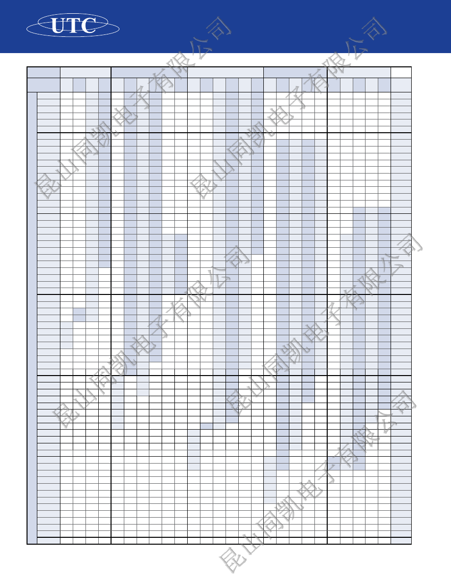
5
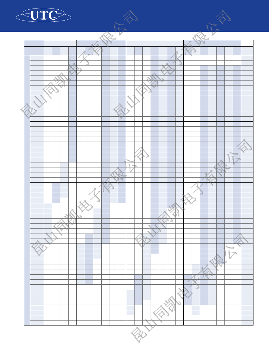
Size
0402
0603
0805
1206
1210
Rated Voltage
(VDC)
16V 25V 50V 100V 16V 25V 50V 100V 200V 250V 16V 25V 50V 100V 200V 250V 16V 50V 100V 200V 250V 16V 50V 100V 200V 250V
EIA
Code
Ca
pacitance
0.5pF
N
N
S
S
S
A
A
A
A
(0R5)
0.6pF
N
N
S
S
S
A
A
A
A
(0R6)
0.7pF
N
N
S
S
S
A
A
A
A
(0R7)
0.8pF
N
N
S
S
S
A
A
A
A
(0R8)
0.9pF
N
N
S
S
S
A
A
A
A
(0R9)
1.0pF
N
N
S
S
S
A
A
A
A
(1R0)
1.2pF
N
N
S
S
S
A
A
A
A
(1R2)
1.5pF
N
N
S
S
S
A
A
A
A
B
B
B
B
(1R5)
1.8pF
N
N
S
S
S
A
A
A
A
B
B
B
B
(1R8)
2.2pF
N
N
S
S
S
A
A
A
A
B
B
B
B
(2R2)
2.7pF
N
N
S
S
S
A
A
A
A
B
B
B
B
(2R7)
3.3pF
N
N
S
S
S
A
A
A
A
B
B
B
B
(3R3)
3.9pF
N
N
S
S
S
A
A
A
A
B
B
B
B
(3R9)
4.7pF
N
N
S
S
S
A
A
A
A
B
B
B
B
(4R7)
5.6pF
N
N
S
S
S
A
A
A
A
B
B
B
B
(5R6)
6.8pF
N
N
S
S
S
A
A
A
A
B
B
B
B
(6R8)
8.2pF
N
N
S
S
S
A
A
A
B
B
B
B
B
(8R2)
10pF
N
N
S
S
S
A
A
A
B
B
B
B
B
C
C
C
100
12pF
N
N
S
S
S
A
A
A
D
B
B
B
B
C
C
C
120
15pF
N
N
S
S
S
A
A
A
D
B
B
B
B
C
C
C
150
18pF
N
N
S
S
S
A
A
A
D
B
B
B
B
C
C
C
180
22pF
N
N
S
S
S
S
S
A
A
A
D
B
B
B
B
C
C
C
C
220
27pF
N
N
S
S
S
S
S
A
A
A
D
B
B
B
B
C
C
C
C
270
33pF
N
N
S
S
S
S
S
A
A
A
D
B
B
B
B
C
C
C
C
330
39pF
N
N
S
S
S
S
S
A
A
A
B
B
B
B
C
C
C
C
390
47pF
N
N
S
S
S
S
S
A
A
A
B
B
B
B
C
C
C
C
470
56pF
N
S
S
S
S
S
A
A
A
B
B
B
B
C
C
C
C
560
68pF
N
S
S
S
S
S
A
A
A
B
B
B
B
C
C
C
C
680
82pF
N
S
S
S
S
S
A
A
A
B
B
B
B
C
C
C
C
820
100pF
N
S
S
S
S
S
A
A
A
B
B
B
B
C
C
C
C
101
120pF
N
S
S
S
A
A
A
B
B
B
B
C
C
C
C
121
150pF
N
S
S
S
A
A
A
B
B
B
B
C
C
C
C
151
180pF
N
N
S
S
S
A
A
A
B
B
B
B
C
C
C
C
181
220pF
N
N
S
S
S
A
A
A
B
B
B
B
C
C
C
C
221
270pF
N
S
S
S
A
A
A
B
B
B
C
C
C
C
C
271
330pF
N
S
S
S
A
A
A
B
B
B
C
C
C
C
C
331
390pF
N
S
S
S
A
A
A
B
B
B
C
C
C
C
C
391
470pF
N
S
S
S
A
A
B
B
B
C
C
C
C
C
C
471
560pF
S
S
S
A
A
B
B
B
C
C
C
C
C
C
561
680pF
S
S
S
A
A
D
B
B
C
C
C
C
C
C
681
820pF
S
S
A
A
D
B
B
C
D
C
C
C
C
821
1000pF
S
S
A
A
B
B
C
G
C
C
C
C
102
1200pF
S
S
B
B
B
B
C
C
C
D
D
122
1500pF
S
S
B
B
B
B
C
C
C
D
D
152
1800pF
S
S
B
B
B
B
D
C
C
D
D
182
2200pF
S
B
B
B
B
D
C
C
D
D
222
2700pF
S
D
D
B
B
C
C
D
D
272
3300pF
S
D
D
B
B
C
C
D
332
3900pF
S
D
D
B
B
C
C
D
392
4700pF
S
D
D
B
B
C
C
472
5600pF
D
B
B
C
C
562
6800pF
D
C
C
C
C
682
8200pF
D
C
C
C
C
822
0.010µF
D
D
C
C
103
0.012µF
D
D
P
C
D
D
123
0.015µF
D
D
P
C
D
D
153
0.018µF
D
183
0.022µF
D
223
0.027µF
D
273
0.033µF
D
333
0.039µF
D
393
0.047µF
473
0.056µF
683
0.068µF
563
0.082µF
823
0.010µF
104
0.012µF
124
NPO-COG DIELECTRIC
5
Note: Please refer to the chart on page 3 for the corresponding thickness designation.
6
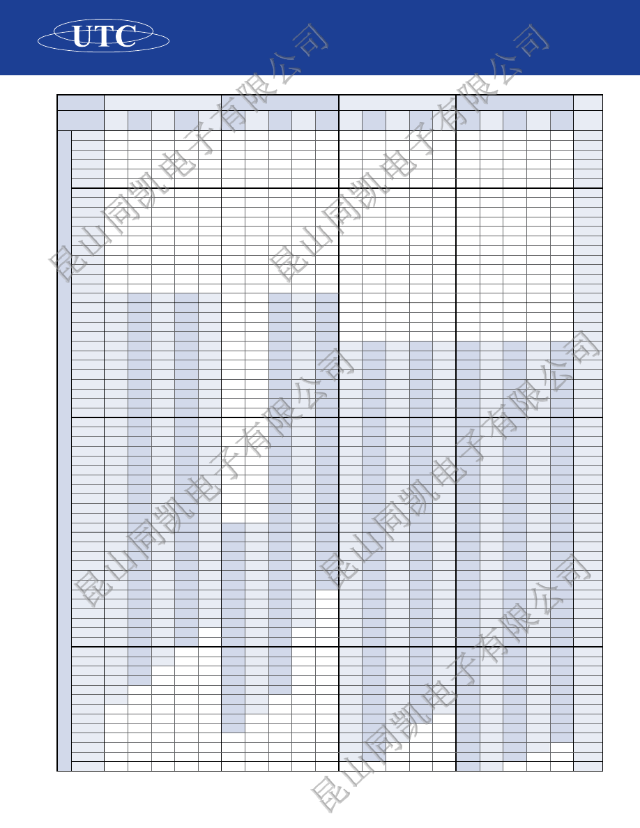
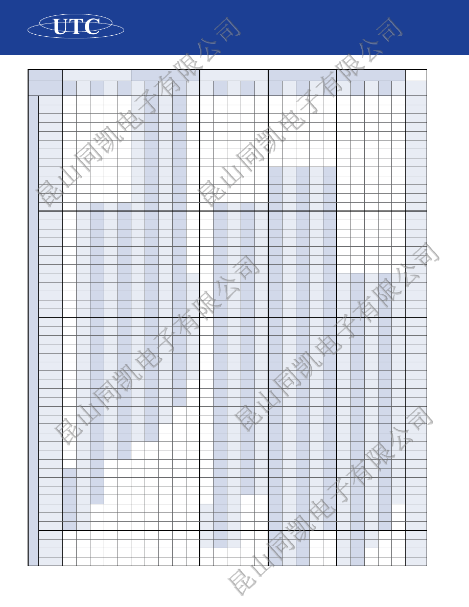
Size
1808
1812
2220
2225
Rated Voltage
(VDC)
25V
50V
100V
200V 250V
25V
50V
100V
200V 250V
25V
50V
100V
200V 250V
25V
50V
100V
200V 250V
EIA
Code
Ca
pacitance
0.5pF
(0R5)
0.6pF
(0R6)
0.7pF
(0R7)
0.8pF
(0R8)
0.9pF
(0R9)
1.0pF
(1R0)
1.2pF
(1R2)
1.5pF
(1R5)
1.8pF
(1R8)
2.2pF
(2R2)
2.7pF
(2R7)
3.3pF
(3R3)
3.9pF
(3R9)
4.7pF
(4R7)
5.6pF
(5R6)
6.8pF
(6R8)
8.2pF
(8R2)
10pF
D
D
D
D
D
D
D
D
100
12pF
D
D
D
D
D
D
D
D
120
15pF
D
D
D
D
D
D
D
D
150
18pF
D
D
D
D
D
D
D
D
180
22pF
D
D
D
D
D
D
D
D
220
27pF
D
D
D
D
D
D
D
D
D
D
D
D
D
D
D
D
D
D
270
33pF
D
D
D
D
D
D
D
D
D
D
D
D
D
D
D
D
D
D
330
39pF
D
D
D
D
D
D
D
D
D
D
D
D
D
D
D
D
D
D
390
47pF
D
D
D
D
D
D
D
D
D
D
D
D
D
D
D
D
D
D
470
56pF
D
D
D
D
D
D
D
D
D
D
D
D
D
D
D
D
D
D
560
68pF
D
D
D
D
D
D
D
D
D
D
D
D
D
D
D
D
D
D
680
82pF
D
D
D
D
D
D
D
D
D
D
D
D
D
D
D
D
D
D
820
100pF
D
D
D
D
D
D
D
D
D
D
D
D
D
D
D
D
D
D
101
120pF
D
D
D
D
D
D
D
D
D
D
D
D
D
D
D
D
D
D
121
150pF
D
D
D
D
D
D
D
D
D
D
D
D
D
D
D
D
D
D
151
180pF
D
D
D
D
D
D
D
D
D
D
D
D
D
D
D
D
D
D
181
220pF
D
D
D
D
D
D
D
D
D
D
D
D
D
D
D
D
D
D
221
270pF
D
D
D
D
D
D
D
D
D
D
D
D
D
D
D
D
D
D
271
330pF
D
D
D
D
D
D
D
D
D
D
D
D
D
D
D
D
D
D
331
390pF
D
D
D
D
D
D
D
D
D
D
D
D
D
D
D
D
D
D
391
470pF
D
D
D
D
D
D
D
D
D
D
D
D
D
D
D
D
D
D
471
560pF
D
D
D
D
D
D
D
D
D
D
D
D
D
D
D
D
D
D
561
680pF
D
D
D
D
D
D
D
D
D
D
D
D
D
D
D
D
D
D
681
820pF
D
D
D
D
D
D
D
D
D
D
D
D
D
D
D
D
D
D
821
1000pF
D
D
D
D
D
D
D
D
D
D
D
D
D
D
D
D
D
D
D
D
102
1200pF
D
D
D
D
D
D
D
D
D
D
D
D
D
D
D
D
D
D
D
D
122
1500pF
D
D
D
D
D
D
D
D
D
D
D
D
D
D
D
D
D
D
D
D
152
1800pF
D
D
D
D
D
D
D
D
D
D
D
D
D
D
D
D
D
D
D
D
182
2200pF
D
D
D
D
D
D
D
D
D
D
D
D
D
D
D
D
D
D
D
D
222
2700pF
D
D
D
D
D
D
D
D
D
D
D
D
D
D
D
D
D
D
D
D
272
3300pF
D
D
D
D
D
D
D
D
D
D
D
D
D
D
D
D
D
D
D
D
332
3900pF
D
D
D
D
D
D
D
D
D
D
D
D
D
D
D
D
D
D
D
392
4700pF
D
D
D
D
D
D
D
D
D
D
D
D
D
D
D
D
D
D
D
472
5600pF
D
D
D
D
D
D
D
D
D
D
D
D
D
D
D
D
D
D
D
562
6800pF
D
D
D
D
D
D
D
D
D
D
D
D
D
D
D
D
D
D
D
682
8200pF
D
D
D
D
D
D
D
D
D
D
D
D
D
D
D
D
D
822
0.010µF
D
D
D
D
D
D
D
D
D
D
D
D
D
D
D
D
D
103
0.012µF
D
D
D
D
D
D
D
D
D
D
D
D
D
D
D
D
123
0.015µF
D
D
D
D
D
D
D
D
D
D
D
D
D
D
D
D
153
0.018µF
D
D
D
D
D
D
D
D
D
D
D
D
D
D
D
183
0.022µF
D
D
D
D
D
D
D
D
D
D
D
D
D
D
D
223
0.027µF
D
D
D
D
D
D
D
D
D
D
D
D
D
D
273
0.033µF
D
D
D
D
D
D
D
D
D
D
D
D
D
333
0.039µF
D
D
D
D
D
D
D
D
D
D
D
D
393
0.047µF
D
D
D
D
D
D
D
D
D
D
473
0.056µF
D
D
D
D
D
D
D
D
D
563
0.068µF
D
D
D
D
D
D
D
D
683
0.082µF
D
D
D
D
D
D
823
0.10µF
D
D
D
D
D
104
0.12µF
D
D
124
NPO-COG DIELECTRIC
6
Note: Please refer to the chart on page 3 for the corresponding thickness designation.
Temperature Coefficient:
±15% ∆C, -55°C to 125°C.
maximum -55 to 125° at WVdc.
Dissipation Factor:
Maximum DF; 25V - 3.5%
Maximum DF; 50V - 2.5%
Maximum DF; 100V - 2.5%
Maximum DF; 250V - 2.5%
Insulation Resistance:
1000ΩF or 100GΩ, whichever is less @ rated
voltage 25°C. At 125°C IR is 10% of 25°C value.
Dielectric Strength:
2.5 times rated voltage D.C.
1.5 times rated voltage for 500V devices.
Aging:
Maximum 2% per decade hour, for X7R.
Test Parameters:
1 kHz and 1 vms if capacitance
< 10
µF
120 Hz and 0.5 vms if capacitance > 10µF
Capacitance Tolerances
Available:
J, K, M
APPLICATION
Suited for By-Pass and Coupling Application, Filtering, D.C. Blocking and Transient Suppression.
PERFORMANCE SPECIFICATIONS
X7R DIELECTRIC
MONOLITHIC CERAMIC CAPACITORS
7
UTC P/N
STYLE
C = MLCC CHIP
C
104
CAPACITANCE
CODE
2 significant
digits are used
plus the third
character then
represents
the number of
zeros to follow
B
VOLTAGE
C = 10V
E = 16V
L = 25V
G = 50V
B = 100V
R = 200V
H = 250V
0805
BODY SIZE
0402
0603
0805
1206
1210
1812
2220
K
TOLERANCE
J = 5%
K = 10%
M = 20%
W
TERMINATION
W = 100%
tin termination
& RoHS - Lead
Free compliant
product
B = Soft
Termination
[consult factory]
T
PACKAGE
STYLE
T = Tape & Reel
X7R
TEMPERATURE
COEFFICIENT
X7R
HOW TO ORDER
Capacitance Change (%)
vs. Temperature (°C)
10
0
-10
-20
-40 -20
0
20
40
60
80 100 120 140
°C
Dissipation Factor
vs. Temperature (°C)
5
4
3
2
1
-50 -25
0
25
50
75 100 125
°C
Capacitance Change (%)
vs. RMS Volts
50
40
30
20
10
0
5
10
15
20
RMS Volts
0.1
.08
.06
.04
Dissipation Factor (%)
vs. RMS Volts
.02
0
1
2
3
4
5
6
7
RMS Volts
Capacitance Change (%)
vs. D.C. Volts
0
20
40
Due 10 voltage effects (pg 4), higher
voltage rating have different curves.
Consult factory for typical curves.
60
5
10
15
20
25
30
35
40
45
50
D.C. Volts
Dissipation Factor
vs. Frequency (Hz)
0
-10
-20
-30
10
3
10
4
10
5
10
6
Hz
These typical curves are for 50 volt parts.
-60
0
X7R
0VDC X7R
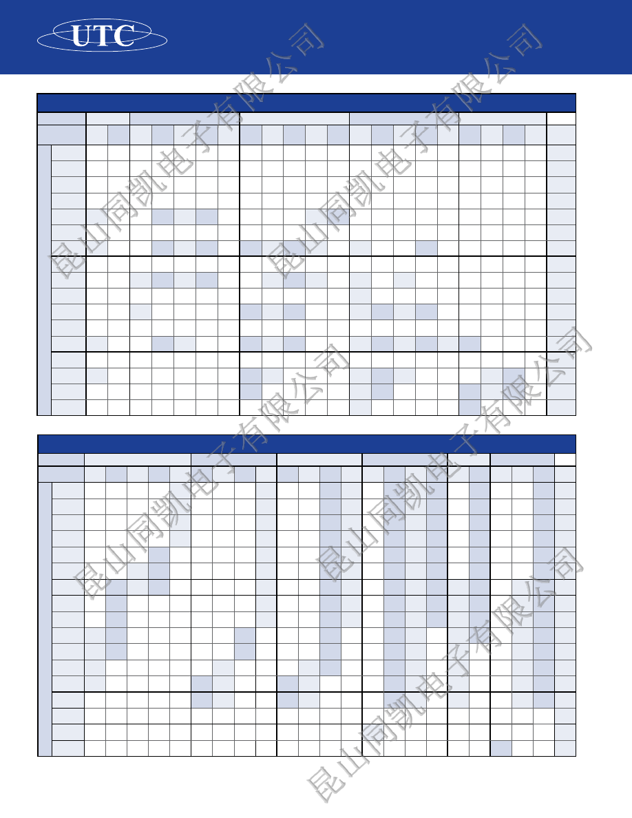
Size
0402
0603
0805
1206
Rated Voltage
(VDC)
10V 16V 25V 50V
10V 16V 25V 50V 100V 200V 10V 16V 25V 50V 100V 200V 250V 10V 16V 25V 50V 100V 200V 250V
EIA
Code
Ca
pacitance
100pF
N
S
S
S
B
B
B
B
101
120pF
N
S
S
S
B
B
B
B
121
150pF
N
S
S
S
B
B
B
B
B
B
B
B
B
151
180pF
N
S
S
S
B
B
B
B
B
B
B
B
B
181
220pF
N
S
S
S
B
B
B
B
B
B
B
B
B
221
270pF
N
S
S
S
B
B
B
B
B
B
B
B
B
271
330pF
N
S
S
S
B
B
B
B
B
B
B
B
B
331
390pF
N
S
S
S
B
B
B
B
B
B
B
B
B
391
470pF
N
S
S
S
B
B
B
B
B
B
B
B
B
471
560pF
N
S
S
S
B
B
B
B
B
B
B
B
B
561
680pF
N
S
S
S
B
B
B
B
B
B
B
B
B
681
820pF
N
S
S
S
B
B
B
B
B
B
B
B
B
821
1000pF
N
S
S
S
B
B
B
B
B
B
B
B
B
102
1200pF
N
S
S
S
B
B
B
B
B
B
B
B
B
122
1500pF
N
S
S
S
B
B
B
B
B
B
B
B
B
152
1800pF
N
S
S
S
B
B
B
B
B
B
B
B
B
182
2200pF
N
S
S
S
B
B
B
B
B
B
B
B
B
222
2700pF
N
S
S
S
B
B
B
B
B
B
B
B
B
272
3300pF
N
S
S
S
B
B
B
B
B
B
B
B
B
332
3900pF
N
S
S
S
B
B
B
B
B
B
B
B
B
392
4700pF
N
S
S
S
B
B
B
B
B
B
B
B
B
472
5600pF
N
S
S
X
B
B
D
D
B
B
B
B
B
562
6800pF
N
S
S
X
B
B
D
D
B
B
B
B
B
682
8200pF
N
S
S
X
B
B
D
D
B
B
B
B
B
822
0.010µF
N
S
S
X
B
B
D
D
B
B
B
B
B
103
0.012µF
N
N
S
X
X
B
B
D
D
B
B
B
B
B
123
0.015µF
N
N
S
X
X
B
B
D
D
B
B
B
C
C
153
0.018µF
N
N
S
X
X
B
B
D
D
B
B
B
C
C
183
0.022µF
N
S
X
X
B
B
D
D
B
B
B
C
C
223
0.027µF
N
S
B
D
D
D
B
B
B
C
C
273
0.033µF
N
S
X
B
D
B
B
B
C
C
333
0.039µF
N
S
X
B
D
B
B
B
C
C
393
0.047µF
N
S
X
B
D
B
B
B
C
C
473
0.056µF
N
S
X
B
D
B
B
B
C
C
563
0.068µF
N
S
X
B
D
B
B
B
C
C
683
0.082µF
N
S
S
X
B
B
D
B
B
D
C
C
823
0.10µF
N
S
S
X
B
B
D
B
B
D
C
C
104
0.12µF
S
S
S
B
D
B
B
D
124
0.15µF
S
S
S
D
D
C
C
G
154
0.18µF
S
S
S
D
C
C
G
184
0.22µF
S
S
D
C
C
G
224
0.27µF
X
X
D
C
D
D
274
0.33µF
X
X
D
C
D
D
334
0.39µF
X
X
D
D
C
J
P
P
394
0.47µF
X
X
D
D
J
J
P
P
474
0.56µF
D
D
J
J
P
P
564
0.68µF
D
D
D
J
J
P
P
684
0.82µF
D
D
D
J
J
P
P
824
1.0µF
D
D
J
J
P
P
105
1.5µF
D
G
155
2.2µF
D
P
225
3.3µF
335
4.7µF
475
X7R DIELECTRIC
8
Note: Please refer to the chart on page 3 for the corresponding thickness designation.
Size
1210
1808
1812
2220
2225
Rated Voltage
(VDC)
25V 50V 100V 200V 250V 25V 50V 100V 200V 250V 25V 50V 100V 200V 250V 25V 50V 100V 200V 250V 25V 50V 100V 200V 250V
EIA
Code
Ca
pacitance
100pF
D
D
D
D
101
120pF
D
D
D
D
121
150pF
D
D
D
D
151
180pF
D
D
D
D
181
220pF
D
D
D
D
221
270pF
D
D
D
D
271
330pF
D
D
D
D
331
390pF
D
D
D
D
391
470pF
D
D
D
D
D
D
D
D
D
471
560pF
D
D
D
D
D
D
D
D
D
561
680pF
D
D
D
D
D
D
D
D
D
681
820pF
D
D
D
D
D
D
D
D
D
821
1000pF
C
C
C
C
D
D
D
D
D
D
D
D
D
D
D
D
D
102
1200pF
C
C
C
C
D
D
D
D
D
D
D
D
D
D
D
D
D
122
1500pF
C
C
C
C
D
D
D
D
D
D
D
D
D
D
D
D
D
152
1800pF
C
C
C
C
D
D
D
D
D
D
D
D
D
D
D
D
D
182
2200pF
C
C
C
C
D
D
D
D
D
D
D
D
D
D
D
D
D
222
2700pF
C
C
C
C
D
D
D
D
D
D
D
D
D
D
D
D
D
272
3300pF
C
C
C
C
D
D
D
D
D
D
D
D
D
D
D
D
D
332
3900pF
C
C
C
C
D
D
D
D
D
D
D
D
D
D
D
D
D
392
4700pF
C
C
C
C
D
D
D
D
D
D
D
D
D
D
D
D
D
D
D
D
D
D
D
472
5600pF
C
C
C
C
D
D
D
D
D
D
D
D
D
D
D
D
D
D
D
D
D
D
D
562
6800pF
C
C
C
C
D
D
D
D
D
D
D
D
D
D
D
D
D
D
D
D
D
D
D
682
8200pF
C
C
C
C
D
D
D
D
D
D
D
D
D
D
D
D
D
D
D
D
D
D
D
822
0.010µF
C
C
C
C
D
D
D
D
D
D
D
D
D
D
D
D
D
D
D
D
D
D
D
103
0.012µF
C
C
C
C
D
D
D
D
D
D
D
D
D
D
D
D
D
D
D
D
D
D
D
123
0.015µF
C
C
C
C
D
D
D
D
D
D
D
D
D
D
D
D
D
D
D
D
D
D
D
153
0.018µF
C
C
C
C
D
D
D
D
D
D
D
D
D
D
D
D
D
D
D
D
D
D
D
183
0.022µF
C
C
C
C
D
D
D
D
D
D
D
D
D
D
D
D
D
D
D
D
D
D
D
223
0.027µF
C
C
C
C
D
D
D
D
D
D
D
D
D
D
D
D
D
D
D
D
D
D
D
273
0.033µF
C
C
C
C
D
D
D
D
D
D
D
D
D
D
D
D
D
D
D
D
D
D
D
333
0.039µF
C
C
C
C
D
D
D
D
D
D
D
D
D
D
D
D
D
D
D
D
D
D
D
393
0.047µF
C
C
D
D
D
D
D
D
D
D
D
D
D
D
D
D
D
D
D
D
D
D
473
0.056µF
C
C
D
D
D
D
D
D
D
D
D
D
D
D
D
D
D
D
D
D
D
D
563
0.068µF
C
C
G
G
D
D
D
D
D
D
D
D
D
D
D
D
D
D
D
D
D
D
683
0.082µF
C
C
G
G
D
D
D
D
D
D
D
D
D
D
D
D
D
D
D
D
D
823
0.10µF
C
C
G
G
D
D
D
D
D
D
D
D
D
D
D
D
D
D
D
D
D
104
0.12µF
C
C
G
G
D
D
D
D
D
D
D
D
D
D
D
D
D
D
D
D
124
0.15µF
C
D
M
M
D
D
D
D
K
K
D
D
D
D
D
D
D
D
D
D
154
0.18µF
C
D
M
M
D
D
K
K
D
D
D
D
D
D
D
D
D
D
184
0.22µF
C
D
M
M
D
D
K
K
D
D
D
D
D
D
D
D
D
D
224
0.27µF
C
G
D
D
K
K
D
D
D
D
D
D
D
D
D
D
274
0.33µF
C
D
G
D
D
K
K
D
D
D
D
D
D
D
D
D
D
334
0.39µF
C
D
M
D
D
K
K
D
D
D
D
D
D
D
D
D
D
394
0.47µF
C
D
M
D
K
K
K
D
D
D
D
D
D
D
D
D
D
474
0.56µF
D
D
M
D
K
D
D
D
D
D
D
D
D
D
D
564
0.68µF
D
D
D
K
K
D
D
D
D
K
D
D
D
D
684
0.82µF
D
D
D
K
K
D
D
D
K
K
D
D
D
D
824
1.0µF
D
D
D
K
K
D
D
D
K
K
D
D
D
D
105
1.5µF
K
K
K
D
D
D
D
D
D
155
2.2µF
K
K
K
D
D
D
D
D
D
225
3.3µF
D
D
D
D
D
335
4.7µF
D
D
D
D
D
475
9
X7R DIELECTRIC
Note: Please refer to the chart on page 3 for the corresponding thickness designation.
Temperature Coefficient:
X5R +15% -15% ∆C, -55°C to 85°C
Y5V +22% -82% ∆C, -30°C to 85°C
Dissipation Factor:
Insulation Resistance:
100ΩF or 10GΩ, whichever is less @ Rated
Voltage 25°C.
Dielectric Strength:
2.5 times rated voltage D.C.
Aging:
X5R Maximum 2.5% per decade hour.
Y5V Maximum 7% per decade hour.
Test parameters:
(X5R)
1 kHz and 1 vms if capacitance
< 10
µF
120 Hz and 0.5 vms if capacitance > 10µF
(Y5V)
1 kHz and 1 vms if capacitance
< 10
µF
120 Hz and 0.5 vms if capacitance > 10µF
1 kHz and 1 vms
Capacitance Tolerance
Available:
M, Z
APPLICATION
Hi-K Dielectric suited for applications where PCB real estate is at a premium and usage is at near room temperature with low DC bias.
PERFORMANCE SPECIFICATIONS
X5R/Y5V DIELECTRIC
MONOLITHIC CERAMIC CAPACITORS
10
UTC P/N
STYLE
C = MLCC CHIP
C
105
CAPACITANCE
CODE
2 significant
digits are used
plus the third
character then
represents
the number of
zeros to follow
L
VOLTAGE
A = 6.3V
C = 10V
E = 16V
L = 25V
G = 50V
B = 100V
0805
BODY SIZE
0402
0603
0805
1206
1210
1812
K
TOLERANCE
K = 10%
M = 20%
Z = -20% / +80%
W
TERMINATION
W = 100%
tin termination
& RoHS - Lead
Free compliant
product
B = Soft
Termination
[consult factory]
T
PACKAGE
STYLE
T = Tape & Reel
X5R
TEMPERATURE
COEFFICIENT
X5R
Y5V
HOW TO ORDER
X5R
Maximum DF;
6.3V~10V - 3.5%
16V~25V - 3.5%
50V - 2.5%
Y5V
Maximum DF;
6.3V~10V - 10%
16V~25V - 7%
50V~100V - 5%
Capacitance Change (%)
vs. Temperature (°C)
20
0
-20
-40
-60
-80
-40 -20
0
20
40
60
80 100 120 140
°C
Dissipation Factor
vs. Temperature (°C)
5
4
3
2
1
-50 -25
0
25
50
75 100 125
°C
Capacitance Change (%)
vs. RMS Volts
50
40
30
20
10
0
5
10
15
20
RMS Volts
0.1
.08
.06
.04
Dissipation Factor
vs.RMS Volts
.02
0
1
2
3
4
5
6
7
RMS Volts
Capacitance Change (%)
vs. D.C. Volts
0
20
40
60
5
10
15
20
25
30
35
40
45
50
D.C. Volts
Dissipation Factor
vs. Frequency (Hz)
0
-10
-20
-30
10
3
10
4
10
5
10
6
Hz
These typical curves are for 50 volt parts.
Y5V
-60
0
Y5V
X5R
Y5V
X5R
Y5V
Size
0402
0603
0805
1206
1210
1812
Rated Voltage
(VDC)
6.3V
10V
16V
25V
50V
10V
16V
25V
50V
16V
25V
50V 100V
10V
25V
50V 100V
50V 100V
10V
50V 100V
EIA
Code
Ca
pacitance
0.010µF
N
S
A
B
B
B
B
C
D
103
0.015µF
N
S
A
B
B
B
B
C
D
153
0.022µF
N
S
A
B
B
B
B
C
D
223
0.033µF
N
S
A
B
B
B
B
C
D
333
0.047µF
N
S
A
B
B
B
B
C
D
473
0.068µF
N
N
S
A
B
B
B
B
C
D
683
0.10µF
N
N
N
S
A
B
B
B
B
C
C
D
D
104
0.15µF
N
S
A
B
B
B
C
C
C
D
D
154
0.22µF
N
S
A
B
B
B
C
C
C
D
D
224
0.33µF
N
N
S
A
B
B
C
C
D
D
334
0.47µF
N
N
S
B
B
B
C
D
D
474
0.68µF
N
S
B
B
B
B
C
D
D
684
1.0µF
N
S
X
B
D
B
B
C
D
D
105
3.3µF
S
X
B
D
C
C
C
D
D
335
10µF
106
22µF
P
226
47µF
K
476
X5R
Size
0402
0603
0805
1206
1210
Rated Voltage
(VDC)
6.3V
10V
6.3V
10V
16V
25V
50V
6.3V
10V
16V
25V
50V
6.3V
10V
16V
25V
50V
6.3V
10V
16V
25V
EIA
Code
Ca
pacitance
0.010µF
103
0.015µF
153
0.022µF
223
0.033µF
333
0.047µF
N
S
S
S
D
D
473
0.068µF
683
1.0µF
N
S
S
S
D
D
D
D
G
P
105
1.5µF
155
2.2µF
S
S
S
S
D
D
D
G
P
225
3.3µF
G
335
4.7µF
S
D
D
D
P
P
P
P
475
6.8µF
685
10µF
N
S
S
D
D
D
P
P
P
P
P
K
106
15µF
156
22µF
N
D
D
P
P
P
K
K
226
47µF
D
P
P
K
K
K
476
100µF
P
K
107
X5R/Y5V DIELECTRIC
11
Note: Please refer to the chart on page 3 for the corresponding thickness designation.
SAFETY CERTIFIED CHIPS
The “S” Series X2/Y3 & X1/Y2
safety capacitors are designed for
applications in; modem, facsimile,
and various other electronic
communication equipment. They
are also well suited for use in
lighting, surge protection, and EMI
filter isolation circuits.
Features & Applications:
• Small size & high cap values
• Surface mountable
• Safety standard approved by
EN132400+A4:01 & UL60950
• RoHS Compliant
• Lead Free
Cap
Value
1808
X1 / Y2
1808
X2 / Y3
1812
X1 / Y2
1812
X2 / Y3
2208
X1 / Y2
2211
X1 / Y2
2220
X1 / Y2
NPO X7R NPO X7R NPO X7R NPO X7R NPO X7R NPO X7R NPO X7R
2R0pF
D
D
D
D
D
5R0pF
D
D
D
D
D
6R8pF
D
D
D
D
D
8R2pF
D
D
D
D
D
100pF
D
D
D
D
D
120pF
D
D
D
D
D
150pF
D
D
D
D
D
180pF
D
D
D
D
D
220pF
D
D
D
D
D
270pF
D
D
D
D
D
330pF
D
D
D
D
D
360pF
D
D
D
D
D
D
390pF
D
D
D
D
D
D
470pF
D
D
D
D
D
D
560pF
D
D
D
D
D
D
680pF
D
D
D
D
D
D
D
820pF
D
D
D
D
D
D
D
101pF
D
D
D
D
D
D
D
121pF
D
D
D
D
D
D
D
131pF
D
D
D
D
D
D
D
D
151pF
D
D
D
D
D
D
D
D
D
D
D
181pF
D
D
D
D
D
D
D
D
D
D
221pF
D
D
D
D
D
D
D
D
D
D
271pF
D
D
D
D
D
D
D
D
D
D
331pF
D
D
D
D
D
D
D
D
D
D
391pF
D
D
D
D
D
D
D
D
D
471pF
D
D
D
D
D
D
D
D
D
561pF
D
D
D
D
D
D
D
D
D
681pF
D
D
D
D
D
D
D
D
D
821pF
D
D
D
D
D
D
D
D
102pF
D
D
D
D
D
D
D
D
D
122pF
D
D
D
D
D
D
D
152pF
D
D
D
D
D
D
182pF
D
D
D
D
D
222pF
D
D
D
D
272pF
D
D
332pF
D
472pF
D
12
Note: Please refer to the chart on page 3 for the corresponding thickness designation.
UTC P/N
STYLE
S = MLCC SAFETY
CERTIFIED CHIP
S
102
CAPACITANCE
CODE
2 significant
digits are used
plus the third
character then
represents
the number of
zeros to follow
X
VOLTAGE
X = X2/Y3
Z = X1/Y2
1808
BODY SIZE
1808
1812
2208
2211
2220
K
TOLERANCE
J = 5%
K = 10%
M = 20%
W
TERMINATION
W = 100%
tin termination
& RoHS - Lead
Free compliant
product
T
PACKAGE
STYLE
T = Tape & Reel
X7R
TEMPERATURE
COEFFICIENT
NPO
X7R
HOW TO ORDER
HIGH VOLTAGE CHIP CAPACITORS
500VDC TO 5000VDC
Dimension
Size
1206
1210
1808
1812
1825
2220
2225
3530
4040
5550
Min Cap
10pF
10pF
10pF
10pF
47pF
47pF
47pF
47pF
47pF
100pF
500V
NPO
1500pF
1800pF
3300pF
.01µF
.022µF
.022µF
.027µF
.068µF
.1µF
.18µF
X7R
.039µF
.047µF
.047µF
.1µF
.33µF
.27µF
.33µF
1.0µF
1.8µF
2.2µF
1000V
NPO
1000pF
2200pF
2200pF
4700pF
.01µF
.01µF
.015µF
.027µF
.056µF
.1µF
X7R
4700pF
.033µF
.01µF
.027µF
.1µF
.1µF
.1µF
.33µF
.56µF
1.0µF
2000V
NPO
220pF
560pF
330pF
1800pF
2700pF
2700pF
3900pF
.015µF
.027µF
.047µF
X7R
1000pF
1800pF
2200pF
4700pF
.012µF
.01µF
.015µF
.068µF
.15µF
.27µF
3000V
NPO
39pF
220pF
1000pF
820pF
1200pF
1200pF
1800pF
.01µF
.018µF
.033µF
X7R
1800pF
1500pF
4700pF
4700pF
5600pF
.027µF
.068µF
.12µF
4000V
NPO
220pF
470pF
680pF
680pF
1000pF
5600pF
.012µF
.018µF
X7R
330pF
680pF
1500pF
1500pF
1500pF
.015µF
.022µF
.047µF
5000V
NPO
390pF
151pF
560pF
3300pF
6800pF
.012µF
X7R
820pF
820pF
1000pF
.01µF
.012µF
.033µF
* TOLERANCE +-.010 or 7% WHICHEVER IS GREATER.
UTC offers a wide variety of sizes, voltages, and capacitance values in our series of High Voltage Ceramic Chips.
Features & Applications:
• Specialized internal electrode designs offer an enhanced product performance.
• Ideally, suited for telecommunication devices in LAN interface (IEEE 802.3) products.
• Performs well as a ballast capacitor for backlighting inverter applications.
• UTC also supports many applications for both custom sizes and voltages beyond those listed.
• RoHS Compliant
• Lead Free
13
UTC P/N
STYLE
C = MLCC CHIP
C
102
CAPACITANCE
CODE
2 significant
digits are used
plus the third
character then
represents
the number of
zeros to follow
T
VOLTAGE
S = 500V
K = 600V
K = 630V
T = 1,000V
W = 2,000V
X = 3,000V
Y = 4,000V
Z = 5,000V
1812
BODY SIZE
1206
1210
1808
1812
1825
2220
2225
3530
4040
5550
K
TOLERANCE
J = 5%
K = 10%
M = 20%
W
TERMINATION
W = 100%
tin termination
& RoHS - Lead
Free compliant
product
B = Soft
Termination
[consult factory]
T
PACKAGE
STYLE
T = Tape & Reel
X7R
TEMPERATURE
COEFFICIENT
NPO
X7R
HOW TO ORDER
Item
Test Condition
Requirements
Visual and Mechanical
---
• No remarkable defect.
• Dimensions to confirm to individual specification sheet
Capacitance
Class I: NPO
Cap
<
100pF 1.0±0.2Vrms, 1MHz±10%
Cap>100pF 1.0±0.2Vrms, 1KHz±10%
Class II: X7R, X5R, Y5R
Cap
<
10µF, 1.0±0.2Vrms, 1KHz±10%
Cap>10µF, 0.5±0.2Vrms, 120Hz±20%
• Shall not exceed the limits given in the detailed spec.
Q/ D.F.
(Dissipation Factor)
NPO:
Cap
>
30pF, Q
>
1000; Cap<30pF, Q
>
400+20C
X7R, X5R:
Rated Voltage D.F.<
Exception of D.F.<
>50V
5.0%
---
---
25V
3.5%
5.0%
0805>1µF, 1210>10µF
7.0%
0603>0.33µF; TT series & Cap>1µF
16V
3.5%
5.0%
0402>0.033µF; 0603>0.15µF;
0805>0.68µF; 1206>2.2µF
10%
TT Series & Cap>1µF
10V
5.0%
10.0% TT Series & Cap>1µF; 0805>10µF
6.3V
10.0%
15.0% 0805>22µF; 1210>100µF
Y5V:
Rated Voltage D.F.<
Exception of D.F.<
>50V
5.0%
---
---
35V
7.0%
---
---
25V
5.0%
7.0%
0603>0.1µF; 0805>µF;
1206>1µF; 1210>4.7µF
9.0%
0402>0.068µF
16V (C<1.0µF) 7.0%
9.0%
0402>0.068µF; 0603>0.68µF
16V (C<1.0µF) 9.0%
12.5% 0805>4.7µF; 1206>10µF; 1210>22µF
10V
12.5%
---
---
6.3V
20.0%
---
---
Dielectric Strength
•
To apply voltage:
(
<
50V) 250%.
•
Duration:
1 to 5 sec.
• Charge & discharge current less than 50mA.
• No evidence of damage or flash over during test.
•
To apply voltage:
100V
>
3 times V DC
200V ~ 300V
>
2 times V DC
500V ~ 999V
>
1.5 times V DC
1000V ~ 5000V
>
1.2 times V DC
• Cut-off, set at 10mA
• TEST= 15 sec.
• RAMP= 0
Dielectric Strength
(for X1/Y2 & X2/Y3)
• To apply 1500 VAC voltage.
•
Duration:
60 sec.
• No evidence of damage or flash over during test.
Insulation Resistance
To apply rated voltage for max. 120 sec.
>
10GΩ or RxC>500 Ω-F whichever is smaller.
Rated Voltage:
100
~ 500V
To apply rated voltage for 60 sec.
>
10GΩ
Rated Voltage:
> 500V
To apply 500V for 60 sec.
>
10GΩ
Temperature Coefficient
With no electrical load.
T.C.
Operating Temp
NPO (COG)
-55~125°C at 25°C
NPO (COJ)
-55~125°C at 25°C
X7R
-55~125°C at 25°C
X5R
-55~85°C at 25°C
Y5V
-55~85°C at 20°C
T.C.
Capacitance Change
NPO (COG)
Within ± 30ppm/°C
NPO (COJ)
Within ± 120ppm/°C
X7R
Within ± 15%
X5R
Within ± 15%
Y5V
Within +30%/-80%
Adhesive Strength
of Termination
•
Pressurizing force:
0402 & 0603:
5N
>0603:
10N
•
Test time:
10±1 sec.
• No remarkable damage or removal of the terminations.
Vibration Resistance
• Vibration frequency: 10~55 Hz/min.
• Total amplitude: 1.5mm
• Test time: 6 hrs. (Two hrs each in three mutually
perpendicular directions.)
• No remarkable damage.
•
Cap change and Q/D.F.:
To meet initial spec.
SPECIFICATIONS &
RELIABILITY TESTS
14
Item
Test Condition
Requirements
Solderability
•
Solder temperature:
235±5°C
•
Dipping time:
2±0.5 sec.
95% min. coverage of all metalized area.
Bending Test
• The middle part of substrate shall be pressurized
by means of the presurrizing rod at a rate of about
1 mm per second until the deflection becomes 1
mm and then the pressure shall be maintained for
5±1 sec.
• Measurement to be made after keeping at room
temp. for 24±2 hrs.
• No remarkable damage.
• Cap change:
NPO:
within ±5.0% or ±0.5pF whichever is larger.
X7R, X5R:
within ±12.5%
Y5V:
within ±30%
(The capacitance change is measured under specified flexture of the
substrate, versus the capacitance measured before the test).
Resistance to
Soldering Heat
•
Solder temperature:
270±5°C
•
Dipping time:
10±1 sec.
•
Preheating:
120 to 150°C for 1 minute before
immerse the capacitor in a eutectic solder.
•
Before intial measurement (Class II only):
Perform 150+0/-10°C for 1 hr and then set for 48±4
hrs at room temp.
• Measurement to be made after keeping at room
temp. for 24±2 hrs. (Class I) or 48±4 hrs. (Class II).
• No remarkable damage.
• Cap change:
NPO:
within ±2.5% or ±0.25pF whichever is larger.
X7R, X5R:
within ±7.5%
Y5V:
within ±20%
•
Q/D.F., I.R. and dielectric strength:
To meet initial requirements.
Temperature Cycle
• Conduct the five cycles according to the temperatures
and time.
Step Temp. (°C)
Time (min.)
1
Min. operating temp. +0/-3
30±3
2
Room temo.
2
~3
3
Max. operating temp. +3/-0
30±3
4
Room temp.
2
~3
• Before initial measurement (Class II only):
Perform 150+0/-10°C for 1 hr and then set for 48±4
hrs at room temp.
• Measurement to be made after keeping at room
temp. for 24±2 hrs. (Class I) or 48±4 hrs. (Class II).
• No remarkable damage.
•
Cap change:
NPO:
within ±2.5% or ±0.25pF whichever is larger.
X7R, X5R:
within ±7.5%
Y5V:
within ±20%
•
Q/D.F., I.R. and dielectric strength:
To meet initial requirements.
Humidity (Steady State)
•
Test temp.:
40±2°C
•
Humidity:
90~95% RH
•
Test time:
500+24/-0 hrs.
• Measurement to be made after keeping at room
temp. for 24±2 hrs. (Class I) or 48±4 hrs. (Class II).
• No remarkable damage.
•
Cap change:
NPO:
within ±5.0% or ±0.5pF whichever is larger.
X7R, X5R:
>
10V, within ±12.5%
6.3V, within ±25%
Y5V:
within ±30%
•
Q/D.F. Value:
NPO:
Cap
>
30pF, Q
>
350; 10pF
<
Cap<30pF, Q
>
275±2.5C.
Cap<10pF; Q
>
200+10C
X7R, X5R:
Rated Voltage D.F.<
Exception of D.F.<
>50V
3.0%
6.0%
0603>0.047µF; 0805>0.18µF;
1206>0.047µF
25V
5.0%
10.0% 0805>1µF, 1210>10µF
14.0% 0603>0.33µF
16V
5.0%
10.0% 0402>0.033µF; 0603>0.15µF;
0805>0.68µF; 1206>2.2µF
10V
7.5%
15.0%
0402>0.033µF; 0603>0.15µF;
0805>0.68µF; 1206>2.2µF,
TT Series & Cap>1µF
6.3V
15.0%
30.0% 0805>10µF; 1210>100µF
Y5V:
Rated Voltage D.F.<
Exception of D.F.<
>50V
7.5%
---
---
35V
10.0%
---
---
25V
7.5%
<10.0% 0603>0.1µF; 0805>0.33µF;
1206>1µF; 1210>4.7µF
<12.5% 0402>0.068µF
16V (C<1.0µF) 10.0%
<12.5% 0402>0.068µF; 0603>0.68µF
16V (C<1.0µF) 12.5%
---
---
10V
15.0%
---
---
6.3V
30.0%
---
---
• I.R.:
>
10V 1GΩ or 50Ω~F whichever is smaller. 6.3V, 10Ω~F
SPECIFICATIONS &
RELIABILITY TESTS
15
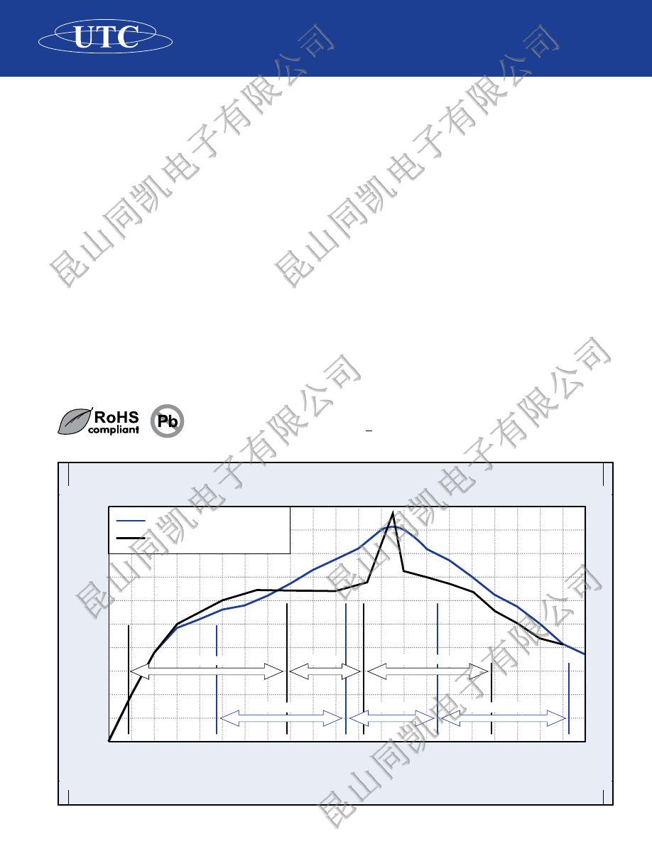
SOLDERING–
ROHS/PB FREE COMPONENTS
The UTC RoHS compliant ceramic chips incorporate
termination bands which are compatible with Pb
Free soldering systems.
PREHEAT CYCLE
The preheat cycle is performed to gradually increase
the component to the higher reflow or wave
solder temperature by minimizing the temperature
differential the component is being exposed to prior
to the reflow cycle beginning.
A higher preheat cycle temperature with wave
soldering can help to reduce thermal shock issues
and can further help if they are preheated from the
bottom side of the board.
REFLOW SOLDER PROFILE
The recommended heating rate will depend on the
body size of each component; however it should not
exceed 3°C / second. While in the reflow phase the
maximum recommended time should not exceed;
40 second time rates @ 230°C. Lastly, the reflow
peak temperature should also not exceed 260°
maximum / 10 seconds. Please refer to the reflow
solder chart for assistance.
WAVE SOLDER PROFILE
Most components that are wave soldered use a
solder at 230°C up to 250°C
Please refer to the charts for guidelines.
COOL DOWN CYCLE
Natural cooling in ambient air is recommended. If
the chips are dipped into a solvent for cleaning,
the temperature difference between the solvent
and the chips must be less than 100°C. This phase
should not be forced, and we recommend a rate
< 6°C / second.
RECOMMENDED
SOLDERING PROFILE
16
25
50
75
100
125
150
175
200
225
250
275
0 20 40 60 80 100 120 140 160 180 200 220 240 260 280 300 320 340 360 380 400 420
Component Temperature / C°
Time/secs
Preheat
Reflow
Cool Down
Preheat
Reflow
Cool Down
Preheat
Wave
Cool Down
Preheat
Wave
Cool Down
Recommended Pb-Free Reflow
Recommended Soldering
SMPS (Switch Mode Power Supply) Capacitors
Manufactured in accordance with military series DSCC Drawing 87106, 88011, and MIL-PRF-49470 • Standard
capacitance range of .056uF to 270uF • Voltages of 50VDC to 500VDC • Case sizes 1, 2, 3, 4, 5, and 6 with
lead styles N, J, and L
High Voltage Radial Capacitors
Manufactured in accordance with military series DSCC Drawings 87046, 87043, 87040, 87114, 87047, 87076,
87044, 87077, 87070 and 87081 • Standard capacitance range of 10pF-0.47uF • Voltages of 1KV to 10KV
Feed-through Discoidal Capacitors
Manufactured in Outside Diameter (OD) sizes of .070” to .600” • Voltages of 50VDC to 3KV • Please contact
factory for other variations, which include size, voltage, termination, dielectric, or special configuration
Planar Capacitor Array
Manufactured in accordance with MIL-STD-1554, MIL-STD-1560A, MIL-STD-1669 • Style SUB-D, Microstyle
SUB-D in accordance with MIL-C-24308
For more information on these products, contact the factory or visit the UTC website at:
http://www.uniontechcorp.com
MILITARY & CUSTOM PRODUCTS
17
Ordering Terminology
Product Family
Voltage
Physical Size
(See DATA Sheet)
Temperature Characteristic
Capacitance
Tolerance
Testing Level
for SMPS and H.V. Radial Capacitors
P
B
4N1
BX
825
K
B
Termination
for Discoidal and Planar Array
Discoidal:
OD & ID (See DATA Sheet)
Array:
Hole Layout per MIL-STD
Note:
This chart outlines the additional UTC product part numbering but please refer to the specific literature for complete information.
Product Family
P = SMPS Capacitors
H = High Voltage
Radial Capacitors
D = Discoidal
A = Planar Array
Voltage
G = 50V
B = 100V
R = 200V
S = 500V
T = 1000V
W = 2000V
X = 3000V
Y = 4000V
Z = 5000V
Temperature
Characteristic
DSCC
EIA
BX
BR
BG
BP
X7R
X7R
X7R
NPO
(COG)
Tolerance
J = ±5 %
K = ±10%
M = ±20%
V = GMV
Z = +80/-20%
Testing Level
A = Electrical
Screening Only
B = MIL-PRF-39014
Group A
C = MIL-PRF-39014
Group B
Termination
P =
Platinum Silver
MILITARY & CUSTOM PRODUCTS
18
UNION TECHNOLOGY CORP.
718 MONTEREY PASS RD., MONTEREY PARK, CA 91754
TEL: (323) 266-6603 FAX: (323) 266-7890
Email: info@uniontechcorp.com
http://www.uniontechcorp.com
Printed in U.S.A.
Catalog 1004