
The information in this publication has been carefully checked and is believed to be
accurate; however, no responsibility is assumed for inaccuracies.
Sanken reserves the right to make changes without further notice to any products herein
in the interest of improvements in the performance, reliability, or manufacturability of its
products. Before placing an order, Sanken advises its customers to obtain the latest
version of the relevant information to verify that the information being relied upon is
current.
Application and operation examples described in this catalog are quoted for the sole
purpose of reference for the use of the products herein and Sanken can assume no
responsibility for any infringement of industrial property rights, intellectual property rights
or any other rights of Sanken or any third party which may result from its use.
When using the products herein, the applicability and suitability of such products for the
intended purpose or object shall be reviewed at the users responsibility.
Although Sanken undertakes to enhance the quality and reliability of its products, the
occurrence of failure and defect of semiconductor products at a certain rate is inevitable.
Users of Sanken products are requested to take, at their own risk, preventative measures
including safety design of the equipment or systems against any possible injury, death,
fires or damages to the society due to device failure or malfunction.
Sanken products listed in this catalog are designed and intended for the use as
components in general purpose electronic equipment or apparatus (home appliances,
office equipment, telecommunication equipment, measuring equipment, etc.).
Before placing an order, the user’s written consent to the specifications is requested.
The use of Sanken products without the written consent of Sanken in the applications
where extremely high reliability is required (aerospace equipment, nuclear power control
systems, life support systems, etc.) is strictly prohibited.
Anti radioactive ray design is not considered for the products listed herein.
This publication shall not be reproduced in whole or in part without prior written approval
from Sanken.
Gallium arsenide is used in some of the products listed in this publication. These
products are dangerous if they are burned or smashed in the process of disposal. It is
also dangerous to drink the liquid or inhale the gas generated by such products when
chemically disposed.
CAUTION / WARNING
•
•
•
•
•
•
•
•
•
•
1

2
●
Regulator
●
High-side power switch
●
Low-side power switch
●
Motor driver IC
●
Hall-Effect IC
●
Custom IC
●
Transistor
●
MOS FET
●
Rectifier Diode for alternator
●
High-voltage diode for igniter
●
Power Zener diode
●
General-purpose diode
●
LED (visible & infrared)
Product Groups

3
[Power Train Control]
●
Engine
• Fuel injection
• Ignition control
• Air ratio control
• Emission purification control
• Idling control
• Knocking and EGR control
• Variable valve timing control
●
Transmission
• Fully electronic control
• CVT control
●
Alternator
[Carbody Control and Safety]
●
4WD
●
4WS
●
ABS
●
Power steering
●
Auto cruising
●
Traction control
●
Stability control
●
Airbag
●
HID Head Lamp
[Compartment Equipment]
●
Automatic air conditioner
●
Power window
●
Keyless entry
●
Panel, Multi-media
• Meter display
• Car audio
• Navigation
• VICS
Applications

SI-3001S
SI-3003S
SI-3101S
SI-3102S
SI-3201S
SI-5151S
SI-5152S
SI-5155S
SI-5153S
SI-5154S
SDH04
SPF5003
SPF5004
SLA2501M
SPF5007
SLA2502M
SPF5002A
SPF5009
SPF5012
SLA4708M
SI-5300
SLA2402M
SLA2403M
2SA1488/1488A 2SA1567
2SA1568
2SC3851
2SC3852
2SC4024
2SC4065
2SC4153
2SD2141
2SD2382
2SD2633
FN812
FP812
MN611S
MN638S
STA315A
STA335A
STA415A
STA461C
STA463C
STA464C
SLA8004
SDA03
SDA04
SDC09
SPF0001
2SK2701
FKV460
FKV460S
FKV560
FKV560S
FKV660
FKV660S
STA508A
STA509A
SMA5113
SLA5027
SDK06
SDK08
SDK09
TFC-561D
4
Contents
■
Application Note for Regulator ICs
■
Dropper Type Regulator ICs
•
With Output ON/OFF Control
•
3-terminal
•
2-output
■
Switching Type Regulator ICs
■
High-side Power Switch ICs
•
With Diagnostic Function
•
With Diagnostic Function , Built-in Zener Diode
•
Surface-mount 2-circuits
•
3-circuits
•
4-circuits
■
Low-side Switch ICs
•
Surface-mount 4-circuits
•
Surface-mount 4-circuits with Output Monitor
■
Stepper-motor Driver IC
■
Full-bridge PWM Motor Driver IC
■
High Voltage Driver ICs for HID Lamps
■
Hall-Effect ICs
■
Custom IC
■
Transistors and MOS FETs
•
Index by Application
•
Index by Load
•
Power Transistor
•
Power Transistor Array
•
Surface-mount Power Transistor Array
•
MOS FET
•
MOS FET Array
•
Surface-mount MOS FET Array
■
Thyristor with built-in reverse diode for HID lamp ignition
■
Rectifier Diode for Alternator
■
High-voltage Diode for Igniter
■
Power Zener Diode
■
General-purpose Diode
■
General-purpose Diode - External Dimensions
■
General-purpose Diode - Taping Specifications
■
General-purpose LEDs
■
General-purpose LED - External Dimensions
■
Index by Part No.
5
6
8
10
14
16
22
26
32
36
40
44
46
48
52
60
62
64
65
66
81
88
92
99
103
106
107
108
109
110
114
116
119
125
130
Application Note for Regulator ICs
■
Temperature and Reliability
Reliability of an IC is generally heavily dependent on
operating temperature. Heat radiation must be fully
considered, and an ample margin should be given
to the radiating area in designing heatsinks. When
mounting ICs on heatsinks, always apply silicone
grease and firmly tighten. Air convection should
actively be used in actual heat dissipation. The
reliability of capacitors and coils, the peripheral
components, is also closely related to temperature.
A high operating temperature may reduce the
service life. Exceeding the allowable temperature
may cause coils to be burned or capacitors to be
damaged. Make sure that output smoothing coils
and input/output capacitors do not exceed their
allowable temperature limit in operation. We
recommend, in particular, to provide an ample
margin for the ratings of coils to minimize heat
generation.
■
Power Dissipation (P
D
)
1. Dropper Type
P
D =
I
O
• [V
IN
(mean) - V
O
]
2. Switching Type
P
D =
V
O
• I
O
( - 1) - V
F
• I
O
(1 - )
Efficiency depends on input/output conditions.
Refer to the efficiency characteristics.
V
O
: Output voltage
V
IN
: Input voltage
I
O
: Output current
: Efficiency
V
F
: Diode forward voltage
■
Heatsink Design
The maximum junction temperature Tj (max) and the
maximum case temperature Tc (max) given in the
absolute maximum ratings are specific to each
product type and must be strictly met. Thus,
heatsink design must be performed in consideration
of the condition of use which affects the maximum
power dissipation P
D
(max) and the maximum
ambient temperature Ta (max). To facilitate heatsink
design, the relationship between these two
parameters is presented in the Ta-P
D
characteristic
graphs. Heatsink design must be performed in the
following steps:
1. Obtain the maximum ambient temperature Ta
(max) (within the set).
2. Obtain the maximum power dissipation P
D
(max).
3. Identify the intersection on the Ta-P
D
characteristic graph and obtain the size of the
heatsink to be used.
The size of a heatsink has been obtained. In actual
applications, a 10 to 20% derating factor is
generally used. Moreover, the heat dissipation
capacity of a heatsink is heavily dependent on how
it is mounted. It is therefore important and
recommended to measure the heatsink and case
temperature in actual operating environments. The
Ta-P
D
characteristics are provided for each product
type for reference purposes.
■
Setting DC Input Voltage
Observe the following precautions when setting the
DC input voltage:
• V
IN (min)
must be at least the set output voltage
plus dropout voltage for the dropper type. It must
be at least the recommended lowest input
voltage for the switching type.
• V
IN (max)
must not exceed the DC input voltage of
the electrical characteristics.
■
Screw Torque
Screw torque should be between 0.588 to 0.686
[N • m] (6.0 to 7.0 [kgf • cm]).
■
Recommended silicone grease
Volatile type silicone grease may produce cracks
after elapse of long term, resulting in reducing heat
radiation effect.
Silicone grease with low consistency (hard grease)
may cause cracks in the mold resin when screwing
the product to a heatsink.
100
V
O
V
IN
5
■
Others
This product may not be connected in parallel.
The switching type may not be used for current
boosting and stepping up voltage.
Type
Suppliers
G746
Shin-Etsu Chemical Co., Ltd.
YG6260
GE Toshiba Silicones Co., Ltd.
SC102
Dow Corning Toray Silicone Co., Ltd.
Output ON
Output OFF
Output ON
Output OFF
Electrical Characteristics
Parameter
Symbol
min
typ
max
Unit
Conditions
Ratings
Output Voltage
Dropout Voltage
Input Voltage
Quiescent Circuit Current
Output Voltage Temperature
Coefficient
( Tj= 25ºC, V
IN
=14V unless otherwise specified)
V
IN
V
IN
=12 to 16V, I
O
= 0.4A
I
O
0.4A
I
O
1.0A
I
O
=0.4A, V
IN
= 6 to 16V
I
O
= 0 to 0.4A
I
O
=5mA, Ta = –10 to +100ºC
I
O
= 0A
V
C
= 2.7V
V
C
= 0.4V
f =100 to 120Hz
6
*
2
30
*
1
V
4.90
5.00
5.10
V
0.5
1.0
V
V
30
mV
±
0.5
100
mV
54
3
dB
10
mA
1.2
A
2.0
V
0.8
V
20
– 0.3
µ
A
mA
V
O
V
DIF
∆
V
O LINE
∆
V
O LOAD
mV/ºC
∆
V
O
/
∆
T
R
REJ
Iq
I
S1
V
C, IH
V
C, IL
I
C, IH
I
C, IL
Ripple Rejection
Overcurrent Protection Starting
Current
Control Voltage
Control Current
Line Regulation
Load Regulation
*
3
*
4
Parameter
Symbol
Unit
Conditions
Ratings
Absolute Maximum Ratings
(Ta = 25ºC)
DC Input Voltage
Output Control Terminal Voltage
Output Current
Power Dissipation
Junction Temperature
Operating Temperature
Storage Temperature
Junction to Case Thermal
Resistance
Junction to Ambient-Air Thermal
Resistance
V
IN
V
C
I
O
P
D1
P
D2
Tj
T
OP
Tstg
j
-c
j
-a
V
With infinite heatsink
Stand-alone without heatsink
Stand-alone without heatsink
V
A
W
W
ºC
ºC
ºC
ºC/W
ºC/W
35
V
IN
1.0
18
1.5
– 40 to +125
– 40 to +100
– 40 to +125
5.5
66.7
*
1
Vc Terminal
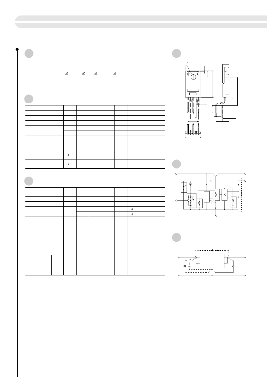
Equivalent Circuit Diagram
Standard Circuit Diagram
Features
●
Output current of 1.0A
●
5-terminal type <output on/off control, variable output voltage (rise only)>
●
Voltage accuracy of
±
2%
●
Low dropout voltage 1V at I
O
1.0A, 0.5V at I
O
0.4A
●
Built-in overcurrent, overvoltage and thermal protection circuits
●
Withstands external electromagnetic noises
●
TO220 equivalent full-mold package
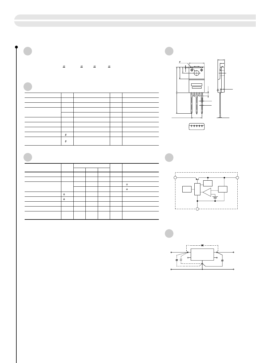
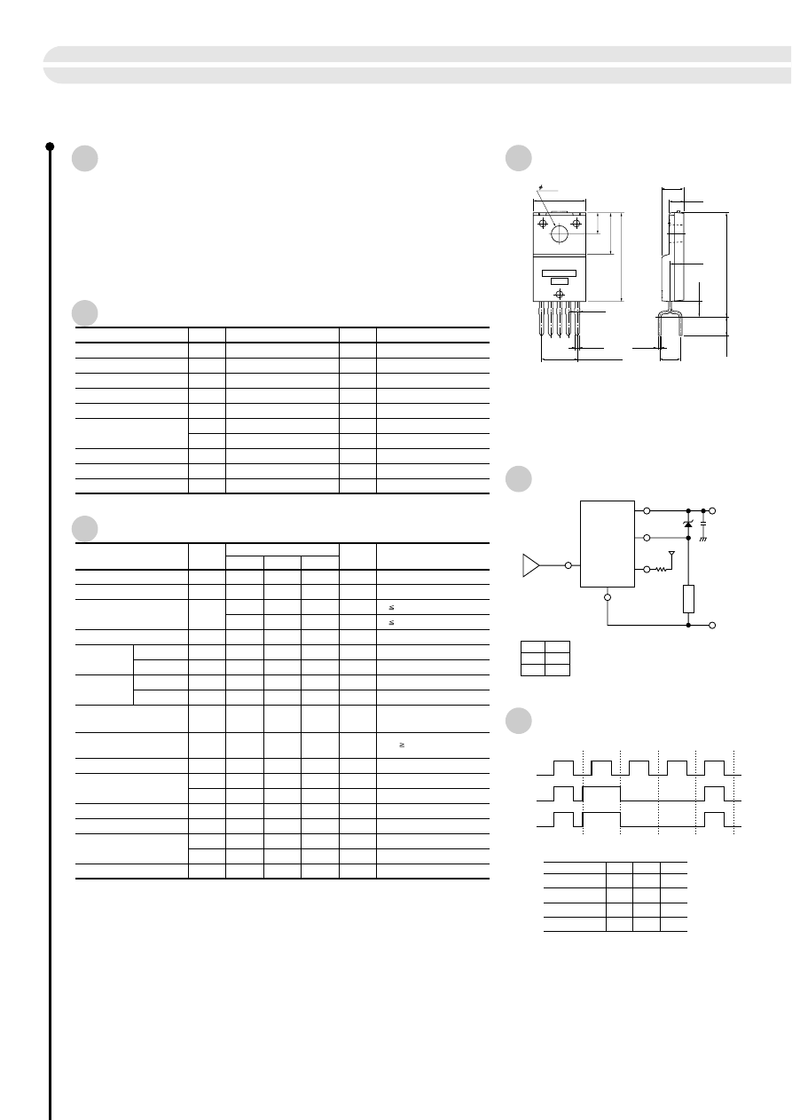
External Dimensions
(unit: mm)
6
a
b
1
2
3
4
5
10.0
±
0.2
3.2
±
0.2
0.5
4.0
±
0.2
7.9
±
0.2
16.9
±
0.3
0.95
±
0.15
0.85
–
0.1
P1.7
±
0.7
• 4=6.8
±
0.7
4.2
±
0.2
2.8
±
0.2
2.6
±
0.1
3.9
±
0.7
8.2
±
0.7
0.45
–
0.1
+
0.2
(2
.0
)
5.0
±
0.6
(8.0)
(17.9)
(4.6)
(4.3)
+
0.2
1. GND
2. V
C
(on/off)
3. Vo
4. Vosense
5. V
IN
a: Part No.
b: Lot No.
(Forming No. 1101)
D
V
DC input
DC output
V
C
1
O
O
IN
5
3
1
SI-3001S
2
4
C
1
C
2
OPEN
GND
1
2
5
3
4
V
O
V
O
sense
R
3
R
4
MIC
Tr
1
R
1
R
2
V
IN
Vc
(on/off)
+
+
Dropper Type Regulator ICs
[With Output ON/OFF Control]
SI-3001S
Notes:
*1. Since P
D
(
max
)
= ( V
IN
– V
O
) • I
O
= 18( W ), V
IN
(
max
)
and I
O
(
max
)
may be limited depending on operating
conditions. Refer to the Ta -P
D
curve to compute the corresponding values.
*2. Refer to the dropout voltage.
*3. I
S1
rating shall be the point at which the output voltage V
O
(V
IN
= 14V, Io = 0.4A) drops to – 5%.
*4. The output control terminal Vc is pulled up inside the IC. Each input level can be directly driven with
LS-TTL ICs. Thus, LS-TTL direct driving is also possible.
a : Pre-regulator
b : Output ON/OFF control
c : Thermal protection
d : Over-input and overcurrent protection
e : Drive circuit
f : Error amplifier
g : Reference voltage
a
b
c
d
e
f
g
Co :
Output capacitor (47 to 100
µ
F, 50V)
C
1
, C
2
: Input capacitors (C
1
: approx. 47
µ
F, C
2
: approx. 0.33
µ
F).
These are required for inductive input lines or long wiring.
Tantalum capacitors are recommended for C
1
and Co,
especially at low temperatures.
D
1
:
Protection diode. Required as protection against reverse
biasing between input and output.
(Recommended diode: Sanken EU2Z.)

7
0
0
0.5
1.0
0.5
0.4
0.3
0.2
0.1
0
0
5
10
15
20
25
30
5.1
5.0
4.9
1.0 (A)
0 (A)
0.4 (A)
I
O
=
0
0
0.5
5.0
4.9
5.5 ( V)
5.1
1.0
30 ( V)
12 to 16 ( V)
V
IN
=
0
0
2
4
6
8
10
1
2
3
4
5
6
7
(
Ω
)
5
(
Ω
)
12
0
0
2
4
6
8
10
15
10
5
I = 0 (A)
o
0
0
0.5
1.0
1.5
2.0
1
2
3
4
5
6
2.5
3.0
(V)
5.5
(V)
14
(V)
20
(V)
30
(V)
10
0
0
1
2
3
1
2
3
4
6
4
5
5
OFF
14 (V)
I = 0 (A)
V =
o
IN
ON
0
0
125
1
2
3
4
6
5
130
135
140
145
150
155
6
(A)
I = 0
V = (V)
o
IN
0
0
5.0
4.9
5.1
100
--50
50
150
5.5(V)
14(V)
16(V)
12(V)
30(V)
V
IN
=
V
IN
— I
OUT
condition
/
0.4
12
(V)
(A)
(A)
(A)
(A)
(A)
(V)
(V)
(V)
(V)
/
1.0
5.5
/
0.4
14
/
0.4
16
/
0
30
0
–20
--30
20
60
40
80
100
0
5
10
15
20
Use G746 silicone grease
(Shin-Etsu Chemical) and
aluminum heatsink.
With infinite heatsink
200•200•2mm (2.3ºC/W)
100•100•2mm (5.2ºC/W)
75•75•2mm (7.6ºC/W)
Without heatsink
10
0
4
3
2
1
5
6
30
20
40
50
Note on Thermal Protection Characteristics:
The thermal protection circuit is intended for protection
against heat during instantaneous short-circuiting. Its
operation, including reliability, is not guaranteed for
short-circuiting over an extended period of time.
Output current I
O
(A)
Output current I
O
(A)
Dropout voltage V
DIF
(V)
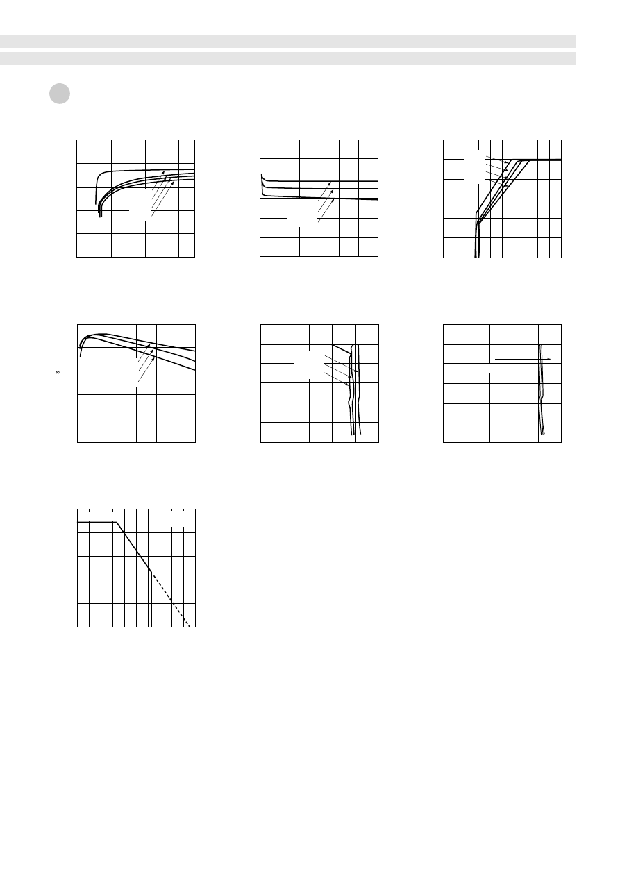
■
Io vs V
DIF
Characteristicsc
■
Line Regulation
Output voltage V
O
(V)
Output voltage V
O
(V)
Output voltage V
O
(V)
Output voltage V
O
(V)
Output voltage V
O
(V)
Output voltage V
O
(V)
Output voltage V
O
(V)
Output voltage V
O
(V)
Input voltage V
IN
(V)
Input voltage V
IN
(V)
Input voltage V
IN
(V)
Input voltage V
IN
(V)
■
Load Regulation
■
Rise Characteristics
■
Quiescent Circuit Current
Quiescent current lq (mA)
■
Overcurrent Protection Characteristics
■
ON/OFF Control Characteristics
Output ON/OFF control voltage V
C
(V)
■
Thermal Protection Characteristics
■
Output Voltage Temperature Characteristics
Ambient temperature Ta (ºC)
Ambient temperature Ta (ºC)
Output current I
O
(A)
Operating temperature Ta (ºC)
Power Dissipation P
D
(W)
■
Ta —P
D
Characteristics
■
Overvoltage Protection Characteristics
Load resistance
Electrical Characteristics
SI-3001S
Electrical Characteristics
Parameter
Symbol
min
typ
max
Unit
Conditions
Ratings
Output voltage
Dropout voltage
Input voltage
Quiescent circuit current
(Tj=25ºC, V
IN
=14V, I
O
=0.5A unless otherwise specified)
V
IN
I
O
0.5A
I
O
0.8A
V
IN
=8 to 16V
I
O
=0 to 0.5A
I
O
=0A
f=100 to 120Hz
6
30
V
4.90
5.00
5.10
V
0.5
1.0
V
V
30
mV
100
mV
54
3
dB
10
mA
0.9
A
V
O
V
DIF
V
O LINE
V
O LOAD
R
REJ
Iq
I
S1
Ripple rejection
Overcurrent protection starting
current
Line regulation
Load regulation
*
3
Parameter
Symbol
Unit
Conditions
Ratings
Absolute Maximum Ratings
(Ta =25ºC)
DC input voltage
Output current
Power Dissipation
Junction temperature
Operating temperature
Storage temperature
Junction to case thermal resistance
Junction to ambient-air thermal
resistance
V
IN
I
O
P
D1
P
D2
Tj
T
OP
Tstg
j
-c
j
-a
V
With infinite heatsink
Stand-alone without heatsink
Stand-alone without heatsink
A
W
W
ºC
ºC
ºC
ºC/W
ºC/W
35
0.8
22
1.8
–40 to +150
–40 to +100
–40 to +150
5.5
66.7
*
2
Equivalent Circuit Diagram
Standard Circuit Diagram
External Dimensions
(unit: mm)
8
Features
●
3-terminal IC regulator with 0.8A output current
●
Voltage accuracy of
±
2%
●
Low Dropout voltage 0.5V at I
O
0.5A, 1V at I
O
0.8A
●
Built-in dropping type overcurrent, overvoltage and thermal protection circuits
●
TO220 equivalent full-mold package
4•P1.7
±
0.15
= 6.8
±
0.15
10
±
0.2
4.2
±
0.2
2.8
±
0.2
2.6
±
0.15
3.2
±
0.2
2 max
0.5
4
±
0.2
7.9
±
0.2
16.9
±
0.3
(13.5)
0.94
±
0.15
0.45
a
b
Terminal connections
1. V
IN
2. (NC)
3. GND
4. (NC)
5. V
O
a: Part No.
b: Lot No.
0.85
+0.2
–0.1
+0.2
–0.1
(root dimensions)
1 2 3 4 5
(Forming No. 1115)
D
V
DC input
DC output
V
C
1
O
O
IN
1
3
SI-3003S
C
1
C
2
5
2
N.C
N.C
4
+
+
V
IN
V
O
1
3
5
GND
TSD
ERR
OCP
DET
REF
DRIVE
Dropper Type Regulator ICs
[3-terminal]
SI-3003S
Notes:
*1. Since P
D
(max)
= (V
IN
– V
O
) • I
O
=22 (W), V
IN
(max)
and I
O
(max)
may be limited depending on operating
conditions. Refer to the Ta —P
D
curve to compute the corresponding values.
*2. Refer to the dropout voltage.
*3. IS1 rating shall be the point at which the output voltage V
O
(V
IN
=14V, I
O
=0.5A) drops to –5%.
Co :
Output capacitor (47 to 100
µ
F, 50V)
C
1
,C
2
: Input capacitors (C
1
: approx. 47
µ
F, C
2
: approx. 0.33
µ
F).
These are required for inductive input lines or long
wiring. Tantalum capacitors are recommended for C
1
and Co, especially at low temperatures.
D
1
:
Protection diode. Required as protection against reverse
biasing between input and output.
(Recommended diode: Sanken EU2Z.)
*
2
*
1
*
2
*
1
*
2
*
1

9
0.2
0.1
0.3
0.4
0.5
0
0
0.2
0.4
0.6
0.8
0
4.9
5.0
5.1
0
5
10
15
20
25
35
30
0
2
1
3
4
6
5
0
2
4
6
10
8
0
0
4.9
5.0
5.1
0.2
0.4
0.6
0.8
I
O
=0A
=0.2A
=0.5A
=0.8A
I
O
=0A
=0.5A
=0.8A
I
O
=0.8A
=0.5A
=0.2A
=0A
I
O
=0.5, 0.8A
=0.2A
=0A
V
IN
=35V
=25V
=14V
=6V
5.0
4.9
5.1
–50
0
50
100
150
V
IN
/ I
O
:
6V / 0.8A
14V / 0.5A
30V / 0A
0
100
50
150
200
250
0
5
10
15
20
25
35
30
0
0
4
3
2
1
5
6
0.5
1.0
1.5
2.0
2.5
V
IN
=6V
14V
35V
25V
2
1
3
4
5
6
0
120
140
160
180
200
V
IN
=6V
I
O
=5mA
10
5
15
20
25
0
–40
0
40
80
100
200 • 200 • 2mm
(2.3ºC/W)
100 • 100 • 2mm
(5.2ºC/W)
75 • 75 • 2mm
(7.6ºC/W)
Note on Thermal Protection Characteristics:
The thermal protection circuit is intended for protection
against heat during instantaneous short-circuiting. Its
operation, including reliability, is not guaranteed for
short-circuiting over an extended period of time.
Output current I
O
(A)
Output current I
O
(A)
Dropout voltage V
DIF
(V)
■
Io vs V
DIF
Characteristics
■
Line Regulation
Output voltage V
O
(V)
Output voltage V
O
(V)
Output voltage V
O
(V)
Output voltage V
O
(V)
Output voltage V
O
(V)
Output voltage V
O
(V)
Input voltage V
IN
(V)
Input voltage V
IN
(V)
Input voltage V
IN
(V)
■
Load Regulation
■
Rise Characteristics
■
Circuit Current
■
Thermal Protection Characteristics
Ground current lg (mA)
■
Overcurrent Protection Characteristics
■
Output Voltage Temperature Characteristics
Ambient temperature Ta (ºC)
Ambient temperature Ta (ºC)
Output current I
O
(A)
Operating temperature Ta (ºC)
Power Dissipation P
D
(W)
■
Ta —P
D
Characteristics
With silicone grease
Heatsink: aluminum
With infinite heatsink
Without heatsink
Electrical Characteristics
SI-3003S
Parameter
Symbol
Unit
Conditions
Ratings
Absolute Maximum Ratings
Electrical Characteristics
Parameter
Symbol
min
typ
max
Unit
Conditions
Ratings
(Ta=25ºC)
DC input voltage
Battery reverse connection
Output control terminal voltage
Output current
Power Dissipation
Output voltage
Dropout voltage
Input voltage
Quiescent circuit current
Overvoltage protection starting
voltage
Thermal protection starting
temperature
(Tj=25ºC, V
IN
=14V unless otherwise specified)
Channel-channel voltage difference
Junction Temperature
Operating temperature
Storage temperature
Junction to case thermal resistance
Junction to ambient-air thermal
resistance
V
IN
V
INB
V
C
V
IN
I
O
=0.05A
I
O
=0.3A
I
O1
0.05A
I
O2
0.4A
V
IN
=6 to 18V, I
O
=0.05A
I
O1
=0 to 0.05A
V
IN
=6 to 18V, I
O
=0.3A
I
O2
=0 to 0.3A
I
O1
=0A, V
C
=0V
V
C
=4.8V
V
C
=3.2V
f =100 to 120Hz
f =100 to 120Hz
I
O1
=0 to 0.05A
I
O2
=0 to 0.3A
6
35
V
4.80
5.00
5.20
V
4.80
5.00
5.20
V
–0.1
0.1
V
1.0
V
1.0
V
10
30
mV
10
30
mV
30
70
mV
40
70
mV
54
dB
54
dB
0.8
mA
0.1
A
0.5
A
4.2
4.5
4.8
V
3.2
3.5
3.8
V
100
µ
A
–100
µ
A
35
V
130
ºC
V
O1
V
O2
V
O
V
DIF1
V
DIF2
V
O LINE1
V
O LINE2
V
O LOAD1
V
O LOAD2
R
REJ1
R
REJ2
Iq
I
(S1) 1
I
(S1) 2
V
CH
V
CL
I
CH
I
CL
V
OVP
T
TSD
I
O1
I
O2
P
D1
P
D2
Tj
T
OP
Tstg
j
-c
j
-a
CH1
CH2
CH1
CH2
CH1
CH2
CH1
CH2
CH1
CH2
Ripple rejection
CH1
CH2
Overcurrent protection
starting current
CH1
CH2
Output control voltage
Output ON
Output OFF
Output ON
Output OFF
Output control current
V
V
One minute
With infinite heatsink
Stand-alone without heatsink
Stand-alone without heatsink
V
A
A
W
W
ºC
ºC
ºC
ºC/W
ºC/W
40
–13
V
IN
0.07
0.4
18
1.5
–40 to +125
–40 to +115
–40 to +125
5.5
66.7
(V
O1
—V
O2
)
Line regulation
Load regulation
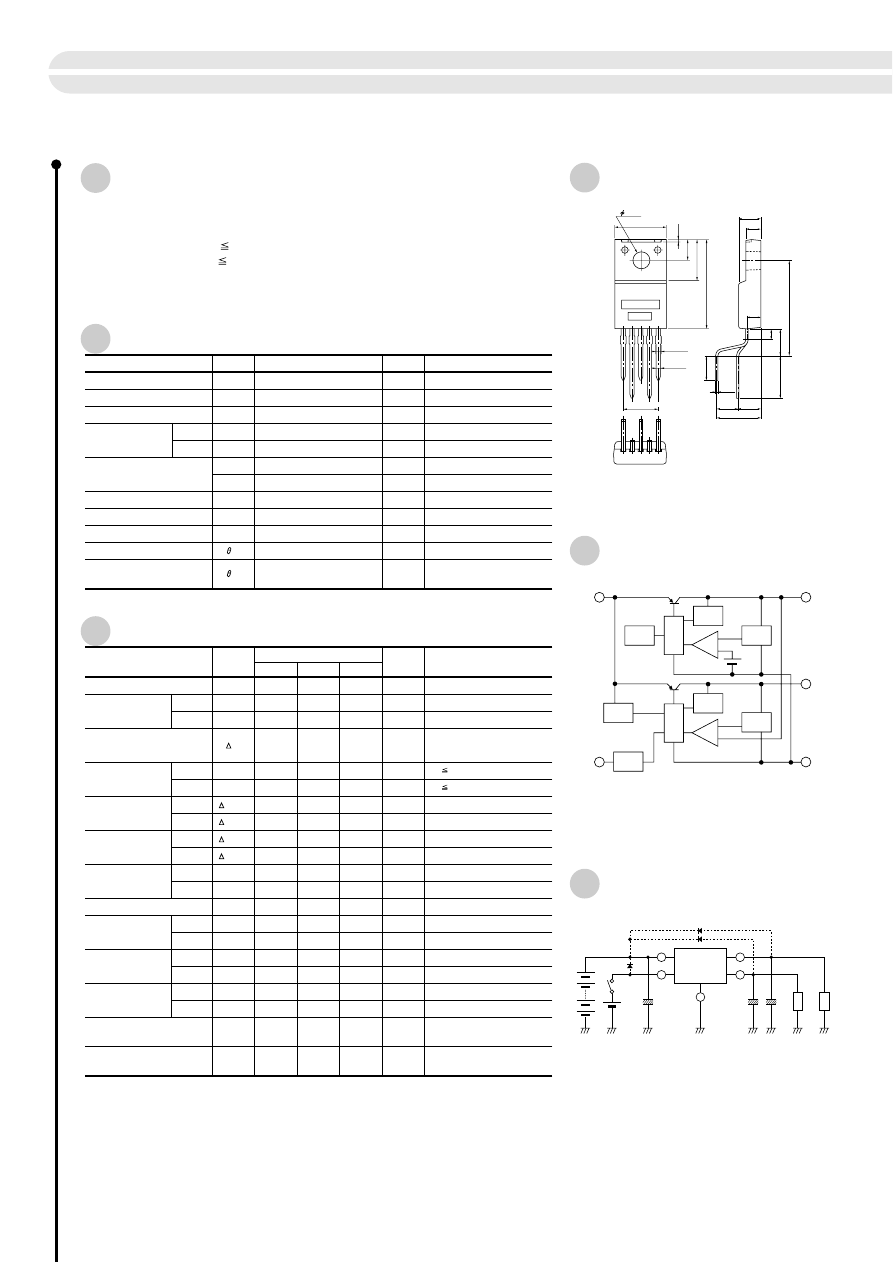
Equivalent Circuit Diagram
Standard Circuit Diagram
External Dimensions
(unit: mm)
Features
●
Single input dual output <sub output (5V/0.07A), main output (5V/0.4A)>
●
Main output can be externally turned ON/OFF (with ignition switch, etc.)
<most suitable as memory backup power supply>
●
Low standby current ( 0.8mA)
●
Low dropout voltage 1V
●
Built-in dropping type overcurrent, overvoltage and thermal protection circuits
●
TO220 equivalent 5-terminal full-mold package
1
2
3
4
5
10.0
3.2
0.5
4.0
7.9
16.9
0.95
0.85
P1.7 • 4 = 6.8
4.2
±
0.2
2.8
±
0.2
2.6
±
0.1
3.9
±
0.7
±
0.7
±
0.15
8.2
±
0.7
0.45
–0.1
+0.2
–0.1
+0.2
(2
.0
)
5.0
±
0.6
(8.0)
(17.9)
(4.6)
(4.3)
1. V
IN
2. V
C
(on/off)
3. GND
4. V
O1
5. V
O2
a: Part No.
b: Lot No.
(Forming No. 1101)
V
IN
V
C
V
O1
V
O2
GND
1
2
4
5
3
REF
DRIVE
DRIVE
DET
OCP
ERR
TSD
OCP
DET
OVP
CONT
ERR
C
IN
V
C
+
D
1
V
IN
1
SI- 3101S
GND
C
O1
V
O2
D
3
2
3
4
5
D
2
V
O1
+
+
C
O2
10
Dropper Type Regulator ICs
[2-output]
SI-3101S
Notes:
*1. Since P
D
(max)
= (V
IN
– V
O
) • I
O1
+ (V
IN
– V
O2
) • I
O2
= 18 (W), V
IN
(max)
, I
O1
(max)
and I
O2
(max)
may be limited
depending on operating conditions. Refer to the Ta—P
D
curve to compute the corresponding values.
*2. Refer to the dropout voltage.
*3. I
S1
rating shall be the point at which the output voltage V
O1
or V
O2
(V
IN
= 14V, I
O1
= 0.05A or I
O2
= 0.3A)
drops to –5%.
*4. Overvoltage protection circuit is built only in CH2 (V
O2
side).
*5. The indicated temperatures are junction temperatures.
*6. All terminals, except V
IN
and GND, are open.
C
O1
:
Output capacitor (47 to 100
µ
F, 50V)
C
O2
:
Output capacitor (47 to 100
µ
F, 50V)
*1 C
IN
:
Input capacitors (approx. 47
µ
F).
Tantalum capacitors are recommended for C
O1
, C
O2
and C
IN
, especially at low temperatures.
*
2
D
1,
D
2,
D
3
: Protection diode.
Required as protection against reverse biasing
between input and output.
(Recommended diode: Sanken EU2Z.)
*
6
*
1
*
1
*
1
*
2
*
3
*
3
*
4
*
5
±
0.2
±
0.2
±
0.3
±
0.2
±
0.2
b
a

0
0.1
0.2
0.3
0.4
0.5
0.6
0.7 0.8
0
1
2
3
4
5
6
(V)
5
(A)
I
= 0
V =
O1
C
4.5V
6V
14V
22V
V =
IN
0
0
5
10
15
20
25
4.9
5.0
5.1
0 mA
50mA
70mA
(A)
I
= 0
O2
(V)
5
V =
C
I
O1
=
0
0
0.05
1
2
3
4
5
6
0.1
0.15
(V)
5
(A)
I
= 0
V =
O2
C
22V
14V
6V
V =
4.5V
0
10
20
30
60
40
50
70
4.9
5.0
5.1
0
(A)
I
= 0
O2
(V)
5
V =
C
V =
IN
6V 14V
22V
0
0.1
0.2
0.3
0.6
0.4
0.5
4.9
5.0
5.1
0
I
= 0
O1
5
V =
C
V
=
IN
6V,14V
22V
0
10
2
4
6
8
0
6
5
4
2
1
3
∞
71.4
Ω
100
Ω
Load resistor
0
20
10
5
0
5
10
15
(A)
I
= 0
O1
(V)
0
V =
c
0
1
2
3
4
5
6
0
5
6
4
3
2
1
V
=
IN
14V, 22V
6V
10
0
20
30
40
1
2
3
4
5
6
V
O1
(V)
5
V =
C
(mA)
I
=
5
I
=
O1
O2
V
O2
0
130
140
150
160
0
1
2
3
4
5
6
(V)
6
V
=
(mA)
I
=
5
I
=
O1
O2
IN
IN
0
--20
--30
20
60
40
80
100
0
5
10
15
20
200 • 200 • 2mm (2.3ºC/W)
100 • 100 • 2mm (5.2ºC/W)
75 • 75 • 2mm (7.6ºC/W)
115
OFF
ON
0
0
5
10
15
20
25
4.9
5.0
5.1
(A)
I
= 0
O1
(V)
5
V =
C
0.5A
0.3A
I
=
O2
0A
11
Output current I
O
(A)
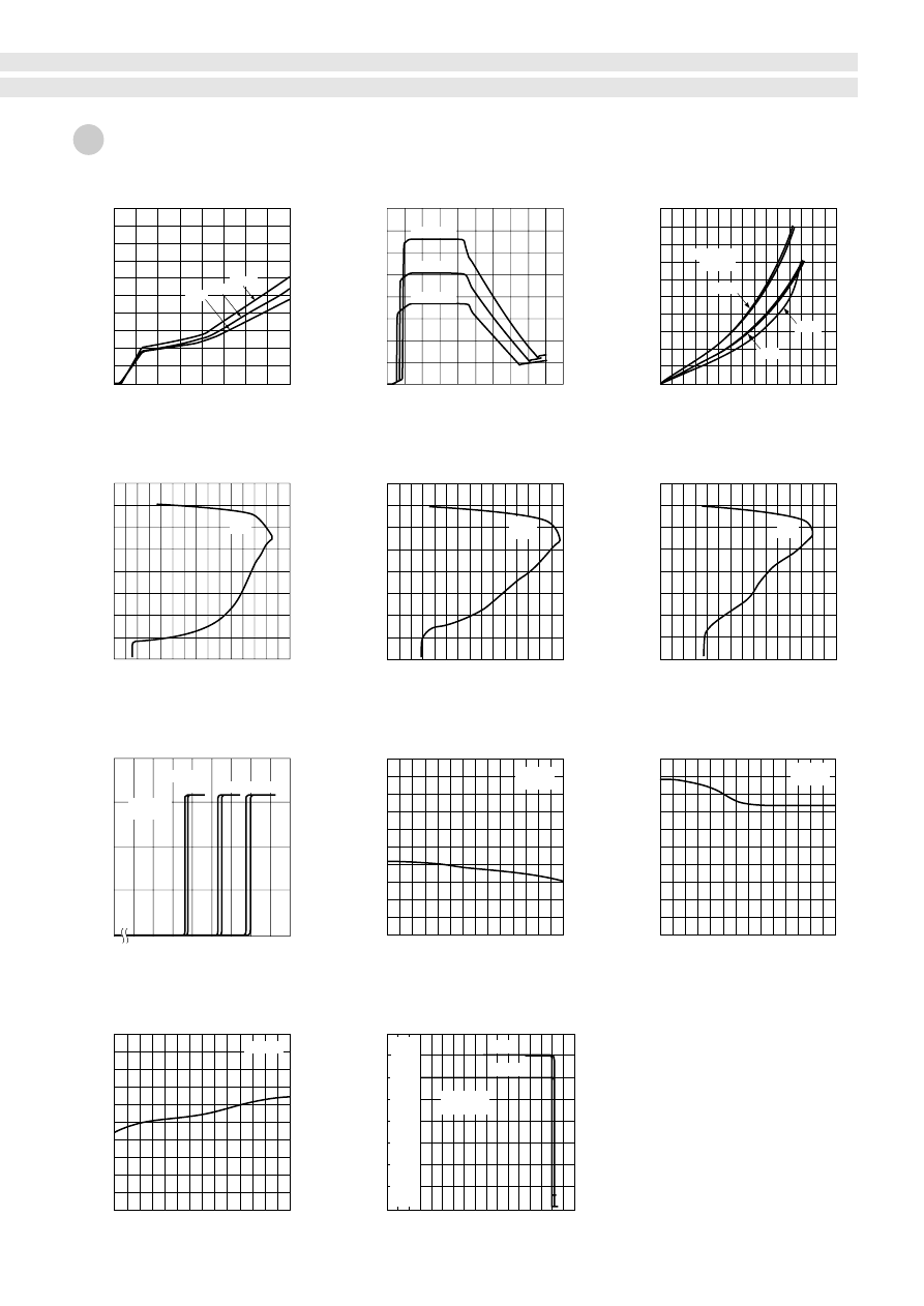
■
Line Regulation (2)
Output voltage V
O
(V)
Output voltage V
O2
(V)
Output voltage V
O
(V)
Output voltage V
O1
(V)
Output voltage V
O1
(V)
Output voltage V
O
(V)
Output voltage V
O
(V)
Input voltage V
IN
(V)
■
Line Regulation (1)
Output voltage V
O
(V)
Input voltage V
IN
(V)
Input voltage V
IN
(V)
Input voltage V
IN
(V)
Input voltage V
IN
(V)
■
Load Regulation (1)
■
Rise Characteristics
■
Quiescent Circuit Current
■
Thermal Protection Characteristics
Quiescent current lq (mA)
■
Overcurrent Protection Characteristics (1)
Output current I
O
(A)
Output voltage V
O2
(V)
■
Overcurrent Protection Characteristics (2)
■
ON/OFF Control Characteristics
Output ON/OFF control voltage V
C
(V)
Ambient temperature Ta (ºC)
Output current I
O
(mA)
Output voltage V
O
(V)
■
Load Regulation (2)
Output current I
O
(A)
Operating temperature Ta (ºC)
Power Dissipation P
D
(W)
■
Ta—P
D
Characteristics
■
Overvoltage Protection Characteristics
With silicone grease G746
(Shin-Etsu Chemical)
Heatsink: aluminum
With infinite heatsink
Without heatsink
Note on Thermal Protection Characteristics:
The thermal protection circuit is intended for protection against heat
during instantaneous short-circuiting. Its operation, including reliability,
is not guaranteed for short-circuiting over an extended period of time.
(A)
(V)
Electrical Characteristics
SI-3101S
Features
●
Single input dual output <sub output (5V/0.04A), main output (5V/0.1A)>
●
Main output can be externally turned ON/OFF (with ignition switch, etc.)
<most suitable as memory backup power supply>
●
Low standby current ( 0.8mA)
●
Low dropout voltage 1V
●
Built-in dropping type overcurrent, overvoltage and thermal protection circuits
●
TO220 equivalent 5-terminal full-mold miniature package
Parameter
Symbol
Unit
Conditions
Ratings
Absolute Maximum Ratings
Electrical Characteristics
External Dimensions
(unit: mm)
Equivalent Circuit Diagram
Standard Circuit Diagram
Parameter
Symbol
min
typ
max
Unit
Conditions
Ratings
(Ta=25ºC)
DC input voltage
Battery reverse connection
Output control terminal voltage
Output current
Power Dissipation
Output voltage
Dropout voltage
Input voltage
Quiescent circuit current
Overvoltage protection starting
voltage
Thermal protection starting
temperature
(Tj = 25ºC, V
IN
= 14V unless otherwise specified)
Junction temperature
Operating temperature
Storage temperature
Junction to case thermal resistance
Junction to ambient-air thermal
resistance
V
IN
V
INB
V
C
V
IN
I
O
= 0.04A
I
O
= 0.1A
I
O1
0.04A
I
O2
0.1A
V
IN
= 6 to 30V, I
O
= 0.04A
I
O1
= 0 to 0.04A
V
IN
= 6 to 30V, I
O
= 0.1A
I
O2
= 0 to 0.1A
I
O1
= 0A, V
C
= 0V
V
C
= 4.8V
V
C
= 3.2V
f
= 100 to 120Hz
f
= 100 to 120Hz
I
O1
=0 to 0.04A
I
O2
=0 to 0.1A
6
30
V
4.80
5.00
5.20
V
4.80
5.00
5.20
V
–0.1
0.1
V
1.0
V
1.0
V
10
50
mV
10
50
mV
30
70
mV
40
70
mV
54
dB
54
dB
0.8
mA
0.06
A
0.15
A
4.2
4.5
4.8
V
3.2
3.5
3.8
V
100
µ
A
–100
µ
A
30
V
151
ºC
V
O1
V
O2
V
O
V
DIF1
V
DIF2
V
O LINE1
V
O LINE2
V
O LOAD1
V
O LOAD2
R
REJ1
R
REJ2
Iq
I
(S1) 1
I
(S1) 2
V
CH
V
CL
I
CH
I
CL
V
OVP
T
TSD
I
O1
I
O2
P
D1
P
D2
Tj
T
OP
Tstg
j
-c
j
-a
CH1
CH2
CH1
CH2
CH1
CH2
CH1
CH2
CH1
CH2
Ripple rejection
CH1
CH2
Overcurrent protection
starting current
CH1
CH2
Output control voltage
Output ON
Output OFF
Output ON
Output OFF
Output control current
V
V
One minute
With infinite heatsink
Stand-alone without heatsink
Stand-alone without heatsink
V
A
A
W
W
ºC
ºC
ºC
ºC/W
ºC/W
35
–13
V
IN
0.04
0.1
22
1.8
–40 to +150
–40 to +105
–40 to +150
5.5
66.7
Line regulation
Load regulation
a
b
1
2
3
4
5
10.0
3.2
0.5
4.0
7.9
16.9
0.95
0.85
P1.7 • 4 = 6.8
4.2
±
0.2
2.8
±
0.2
2.6
±
0.1
3.9
±
0.7
±
0.7
±
0.7
8.2
±
0.7
0.45
–0.1
+0.2
–0.1
+0.2
(2
.0
)
5.0
±
0.6
(8.0)
(17.9)
(4.6)
(4.3)
1. V
IN
2. V
C
(on/off)
3. GND
4. V
O1
5. V
O2
a: Part No.
b: Lot No.
(Forming No. 1101)
V
IN
V
C
V
O1
V
O2
GND
1
2
4
5
3
REF
DRIVE
DRIVE
DET
OCP
ERR
TSD
OCP
DET
OVP
CONT
ERR
C
IN
V
C
+
D
1
V
IN
1
SI- 3102S
GND
C
O1
V
O2
D
3
2
3
4
5
D
2
V
O1
+
+
C
O2
12
Dropper Type Regulator ICs
[2-output]
SI-3102S
Notes:
*1. Since P
D
(max)
= (V
IN
– V
O
) • I
O1
+ (V
IN
– V
O2
) • I
O2
= 22 (W), V
IN
(max)
, I
O1
(max)
and I
O2
(max)
may be limited
depending on operating conditions. Refer to the Ta—P
D
curve to compute the corresponding values.
*2. Refer to the dropout voltage.
*3. I
S1
rating shall be the point at which the output voltage V
O1
or V
O2
(V
IN
= 14V, I
O1
= 0.04A or I
O2
= 0.1A)
drops to –5%.
*4. Overvoltage protection circuit is built only in CH2 (V
O2
side).
*5. The indicated temperatures are junction temperatures.
*6. All terminals, except V
IN
and GND, are open.
C
O1
:
Output capacitor (47 to 100
µ
F, 50V)
C
O2
:
Output capacitor (47 to 100
µ
F, 50V)
*1 C
IN
:
Input capacitors (approx. 47
µ
F).
Tantalum capacitors are recommended, for C
O1
,
C
O2
and C
IN
, especially at low temperatures.
*
2
D
1,
D
2,
D
3
: Protection diode.
Required as protection against reverse biasing
between input and output.
(Recommended diode: Sanken EU2Z.)
*
6
*
1
*
1
*
1
*
2
*
3
*
3
*
4
*
5
Channel-channel voltage difference
(V
O1
—V
O2
)
±
0.2
±
0.2
±
0.2
±
0.2
±
0.3
±
0.15

0
4.90
4.95
5.00
5.05
5.10
4.85
5
10
15
20
25
30
35
0
4.90
4.95
5.00
5.05
5.10
4.85
5
10
15
20
25
30
35
0
4.90
4.95
5.00
5.05
5.10
4.85
10
20
30
50
40
V
IN
= V
C
I
O2
= 5mA
V
IN
= V
C
I
O1
= 5mA
V
C
= 0V
I
O1
= 0A
0A
20mA
40mA
I
O1
=
0A
50mA
100mA
I
O2
=
V
IN
= V
C
6V
14V
30V
V
IN
=
0
4.90
4.95
5.00
5.05
5.10
4.85
20
40
60
100
80
0
2
1
3
4
5
6
0
20
40
60
120
100
80
0
1
2
3
4
5
6
0
0.1
0.2
0.5
0.4
0.3
26
1
2
3
4
5
6
0
28
30
38
36
34
32
0
2
3
4
5
6
0
1
1
2
3
5
6
7
4
0
4
6
8
10
12
0
2
5
10
15
25
30
35
20
V
IN
= V
C
V
IN
= V
C
I
O2
= 5mA
V
IN
= V
C
I
O1
= 5mA
V
IN
= V
C
I
O2
= 5mA
0
1
2
3
4
5
6
0
1
2
6
5
4
3
V
IN
= 14V
I
O2
= 5mA
100
1
2
3
4
5
6
0
120
140
240
220
200
180
–40
5
10
15
20
25
0
–20 0
20
160
140
120
60 80 100
40
V
IN
= 6V
I
O1
= I
O2
= 5mA
6V,14V
30V
V
IN
=
6V
14V
30V
V
IN
=
6V
14V
30V
V
IN
=
I
O1
= 0A
20mA
40mA
200
• 200 • 2mm
(2.3ºC/W)
100
• 100 • 2mm
(5.2ºC/W)
75 • 75 • 2mm
(7.6ºC/W)
OFF
ON
13
Output current I
O
(mA)
■
Line Regulation (2)
Output voltage V
O
(V)
Output voltage V
O2
(V)
Output voltage V
O
(V)
O
utput voltage V
O1
(V)
Output voltage V
O1
(V)
Output voltage V
O
(V)
Output voltage V
O
(V)
Input voltage V
IN
(V)
■
Line Regulation (1)
Output voltage V
O
(V)
Input voltage V
IN
(V)
Input voltage V
IN
(V)
Input voltage V
IN
(V)
Input voltage V
IN
(V)
■
Load Regulation (1)
■
Rise Characteristics
■
Quiescent Circuit Current
■
Thermal Protection Characteristics
Quiescent current lq (mA)
■
Overcurrent Protection Characteristics (1)
Output current I
O2
(A)
Output voltage V
O2
(V)
■
Overcurrent Protection Characteristics (2)
■
ON/OFF Control Characteristics
Output ON/OFF control voltage V
C
(V)
Ambient temperature Ta (ºC)
Output current I
O
(mA)
Output voltage V
O
(V)
■
Load Regulation (2)
Output current I
O
(mA)
Operating temperature Ta (ºC)
Power Dissipation P
D
(W)
■
Ta—P
D
Characteristics
■
Overvoltage Protection Characteristics
With silicone grease G746
(Shin-Etsu Chemical)
Heatsink: aluminum
With infinite heatsink
Without heatsink
Note on Thermal Protection Characteristics:
The thermal protection circuit is intended for protection against heat
during instantaneous short-circuiting. Its operation, including reliability,
is not guaranteed for short-circuiting over an extended period of time.
V
O1
V
O2
Electrical Characteristics
SI-3102S
Features
●
Output current of 3A (Ta = 25ºC, V
IN
= 8 to 18V)
●
High efficiency of 82% (V
IN
= 14V, I
O
= 2A)
●
Requires 5 external components only
●
Built-in reference oscillator (60kHz)
●
Phase internally corrected
●
Output voltage internally corrected
●
Built-in overcurrent and thermal protection circuits
●
Built-in soft start circuit
Parameter
Symbol
Unit
Conditions
Ratings
Absolute Maximum Ratings
Electrical Characteristics
Recommended Operating Conditions
External Dimensions
(unit: mm)
Standard Circuit Diagram
Parameter
Symbol
min
typ
max
min
typ
max
Unit
Conditions
Ratings
(Ta=25ºC)
Input voltage
Output voltage
SW
OUT
terminal voltage
Power Dissipation
Output voltage
Load regulation
Line regulation
Discharge resistance
(V
IN
= 14V, I
OUT
= 2A, Tj = 25ºC unless otherwise specified)
Junction temperature
Storage temperature
Junction to case thermal resistance
Junction to ambient-air thermal
resistance
V
IN
I
O
V
SWOUT
V
O
V
IN
= 8 to 18V
V
SSL
= 0.2V
V
IN
= 0V
4.80
5.00
82
50
60
5
3.1
5.20
100
V
50
mV
0.2
25
200
35
V
15
µ
A
k
Ω
mV
V
O LINE
V
O LOAD
Efficiency
I
O
= 0.5 to 3A
%
Oscillation frequency
70
kHz
f
OSC
Quiescent circuit current
I
O
= 0A
10
mA
Iq
Overcurrent protection starting
current
A
I
S
V
SSL
I
SSL
R
DIS
P
D1
P
D2
Tj
Tstg
j
-c
j
-a
Low level voltage
Source current when low
Soft
start
terminal
V
A
With infinite heatsink
Stand-alone
V
W
W
ºC
ºC
ºC/W
ºC/W
35
3
–1
22
1.8
–40 to +150
–40 to +125
5.5
66.7
Notes:
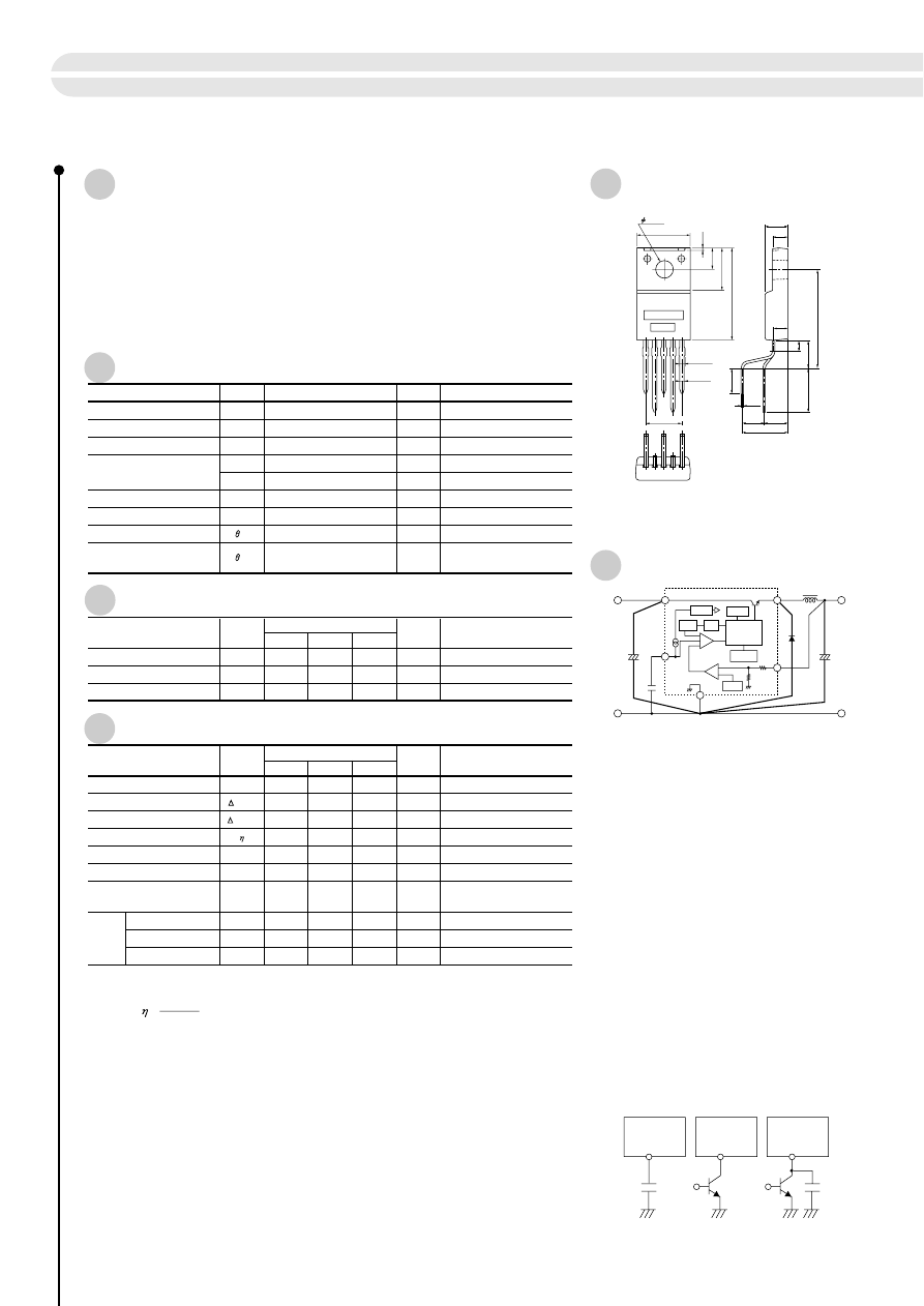
*1. Efficiency is calculated by the following equation:
*2. A dropping-type overcurrent protection circuit is built in the IC.
*3. An external voltage may not be applied to the soft start terminal. As shown in the diagram to the
right, use this IC in the soft start mode with a capacitor or in the open-collector drive mode with a
transistor. Leave the soft start terminal open when not using it since it is already pulled up in the IC.
a
b
1
2
3
4
5
10.0
3.2
0.5
4.0
7.9
16.9
0.95
0.85
P1.7 •4 = 6.8
4.2
±
0.2
2.8
±
0.2
2.6
±
0.1
3.9
8.2
±
0.7
±
0.7
0.45
–0.1
+0.2
–0.1
+0.2
(2
.0
)
5.0
±
0.6
(8.0)
(17.9)
(4.6)
(4.3)
1. V
IN
2. SW
OUT
3. GND
4. V
S
5. SS
a: Part No.
b: Lot No.
(Forming No. 1101)
Parameter
Symbol
Unit
Conditions
Ratings
Input voltage
Output current
Operating temperature
V
IN
I
O
Top
V
A
Ta—P
D
characteristics
ºC
8
0.5
–40
18
3
+85
14
Switching Type Regulator ICs SI-3201S
V
O
• I
O
V
IN
• I
IN
= • 100 (%)
SS
5
SS
C
3
C
3
5
SS
5
SI-3201S
SI-3201S
SI-3201S
SI-3201S
V
IN
V
IN
C
1
C
3
C
2
C
1
: 1000
µ
F
C
2
: 1000
µ
F
L
1
: 250
µ
H
D
1
: RK46 (Sanken)
V
O
SW
OUT
SW Tr
L
1
D
1
V
S
GND
GND
GND
5
3
4
2
1
SS
+
+
a
e
d
b
g
c
h
i
f
a: Internal power supply
b: Thermal protection
c: Reference oscillator
d: Reset
e: Latch & driver
f : Comparator
g: Overcurrent protection
h: Error amplifier
i : Reference voltage
Cautions:
(1) A high-ripple current flows through
C
1
and
C
2
. Use high-ripple
type
1000
µ
F
or higher capacitors with low internal resistance.
Refer to the respective data books for more information on
reliability and electrical characteristics of the capacitor.
(2)
C
3
is a capacitor used for soft start.
(3)
L
1
should be a choke coil with a low core loss for switching
power supplies.
(4) Use a Schottky barrier diode for
D
1
and make sure that the
reverse voltage applied to the 2nd terminal (SW
OUT
terminal) is
within the maximum ratings (–1V). If you use a fast-recovery
diode, the recovery voltage and the ON forward voltage may
cause a reversed-bias voltage exceeding the maximum ratings
to be applied to the 2nd terminal (SW
OUT
terminal). Applying a
reversed-bias voltage exceeding the maximum rating to the
2nd terminal (SW
OUT
terminal) may damage the IC.
(5) The 4th terminal (
V
S
) is an output voltage detection terminal.
Since this terminal has a high impedance, connect it to the
positive (+) terminal of
C
2
via the shortest possible route.
(6) Leave the 5th terminal (soft start terminal) open when not
using it. It is pulled up internally.
(7) To ensure optimum operating environment, connect the high-
frequency current line with minimum wiring length.
*
1
*
3
*
2
±
0.2
±
0.2
±
0.2
±
0.2
±
0.3
±
0.15
±
0.7
±
0.7
= 10V
V 18V
IN
=
7V
=
0
4.85
0.5
1.0
1.5
2.0
2.5
3.0
4.90
4.95
5.00
5.05
5.10
5.15
4.85
4.90
4.95
5.00
5.05
5.10
0
5
10
15
20
25
30
35
I 0A
=
o
1A
=
2A
=
3A
=
0
40
50
60
70
80
90
0.5
1.0
1.5
2.0
2.5
3.0
=
10V
V 18V
IN
=
7V
=
0
0
6
5
4
3
2
1
2
4
6
8
10
I 0A
=
o
1A
2A
3A
=
=
=
0
6
5
4
3
2
1
0
1.0
2.0
3.0
4.0
5.0
T 100, 25, 20ºC
C
=
--
+
0
0
6
5
4
3
2
1
1.0
2.0
3.0
4.0
5.0
V 18V
=
IN
10V
7V
=
=
–40
0
40
80
120
160
10
0
5
15
20
25
15
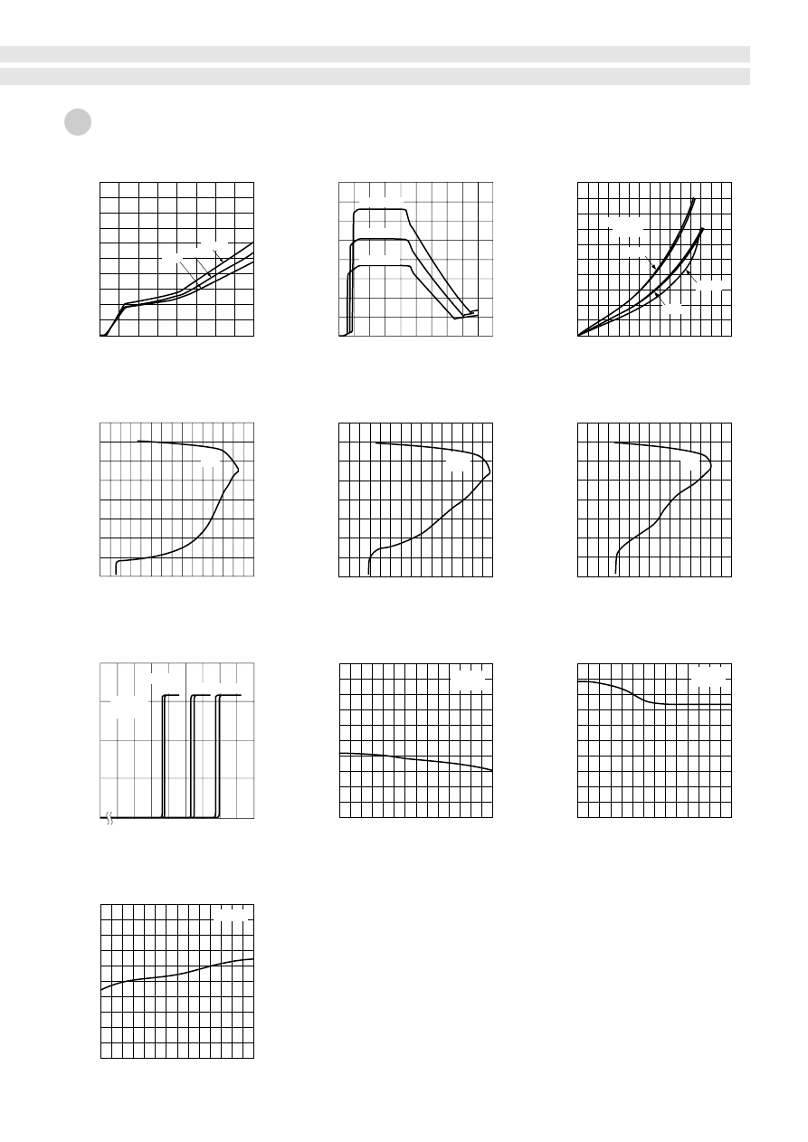
Output current I
O
(A)
■
Line Regulation
Output voltage V
O
(V)
Output voltage V
O
(V)
Output voltage V
O
(V)
Output voltage V
O
(V)
Input voltage V
IN
(V)
Input voltage V
IN
(V)
■
Load Regulation
■
Rise Characteristics
■
Overcurrent Protection Characteristics
Output current I
O
(A)
Output voltage V
O
(V)
■
Overcurrent Protection Temperature Characteristics
■
Efficiency Curve
Output current I
O
(A)
Output current I
O
(A)
Operating temperature Ta (ºC)
Power Dissipation P
D
(W)
■
Ta —P
D
Characteristics
With silicone grease
Heatsink: aluminum
With infinite heatsink
Efficiency (%)
Electrical Characteristics
SI-3201S

Parameter
Symbol
Unit
Conditions
Ratings
Absolute Maximum Ratings
Electrical Characteristics
Parameter
Symbol
min
typ
max
Unit
Conditions
Ratings
(Ta=25ºC)
Power supply voltage
Input terminal voltage
DIAG terminal voltage
Collector-emitter voltage
Power Dissipation
Input voltage
Input current
Operating power supply voltage
Quiescent circuit current
Thermal protection starting
temperature
Minimum load inductance
Open load detection resistor
Output transfer time
DIAG output voltage
DIAG output transfer time
(Ta=25ºC unless otherwise specified)
Saturation voltage of output
transistor
Junction temperature
Operating temperature
Storage temperature
V
B
V
IN
V
DIAG
V
Bopr
V
Bopr
= 14V, V
IN
= 0V
I
O
1.0A, V
Bopr
= 6 to 16V
I
O
1.8A, V
Bopr
= 6 to 16V
V
Bopr
= 6 to 16V
V
Bopr
= 6 to 16V
V
IN
= 5V
V
IN
= 0V
V
Bopr
= 14V, V
O
= V
Bopr
–1.5V
V
Bopr
= 6 to 16V
V
Bopr
= 14V, I
O
= 1A
V
Bopr
= 14V, I
O
= 1A
V
CC
= 6V
V
CC
= 6V, I
DD
= 2mA
V
Bopr
= 14V, I
O
= 1A
V
Bopr
= 14V, I
O
= 1A
V
5
12
6.0
30
mA
0.5
V
1.0
V
V
B
V
0.8
V
1
mA
145
30
8
30
15
30
6
0.3
30
30
mA
125
ºC
k
Ω
µ
s
µ
s
V
V
µ
s
µ
s
Iq
Output leak current
V
CEO
= 16V
2.0
–0.3
–0.1
2
mA
I
O
, leak
V
CE (sat)
V
IH
V
IL
I
IH
I
IL
T
TSD
Overcurrent protection starting
current
1.9
A
I
S
Ropen
T
ON
T
OFF
4.5
1
V
DH
V
DL
T
PLH
T
PHL
mH
L
V
CE
P
D1
P
D2
Tj
T
OP
Tstg
Output ON
Output OFF
Output ON
Output OFF
V
V
With infinite heatsink (Tc
= 25ºC)
Stand-alone without heatsink
(Tc
= 25ºC)
V
V
W
W
ºC
ºC
ºC
40
–0.3 to V
B
6
40
Output current
I
O
A
1.8
18
1.5
–40 to +125
–40 to +100
–40 to +125
Standard Circuit Diagram
Diagnostic Function
External Dimensions
(unit: mm)
Features
●
Built-in diagnostic function to detect short and open circuiting of loads and
output status signals
●
Low saturation PNP transistor use
●
Allows direct driving using LS-TTL and C-MOS logic levels
●
Built-in overcurrent and thermal protection circuits
●
Built-in protection against reverse connection of power supply
●
TO220 equivalent full-mold package not require insulation mica
SI-5151S
PZ
DIAG
5.1k
Ω
GND
1
4
3
5
2
V
IN
V
IN
V
O
H
H
L
L
V
O
V
CC
V
B
Load
LS-TTL
or
CMOS
V
IN
V
O
DIAG
Normal
Normal
Open load
Overheat
Shorted load
Truth table
1. GND
2. V
IN
3. V
O
4. DIAG
5. V
B
a: Part No.
b: Lot No.
(Forming No. 1123)
V
IN
DIAG
Open load
Normal
Mode
Shorted load
Overheat
L
H
V
O
L
H
L
H
L
H
H
H
H
H
L
H
L
L
L
L
L
H
L
L
L
L
●
DIAG output will be undetermined when a voltage
exceeding 25V is applied to V
B
terminal.
Note:
* The rule of protection against reverse connection of power supply is V
B
= –13V, one minute
(all terminals except, V
B
and GND, are open).
16
High-side Power Switch ICs
[With Diagnostic Function]
SI-5151S
10
2.6
4.2
2.8
3.2
4
7.9
20
max
3.6
16.9
P1.7 • 4 = 6.8
0.94
4
0.85
0.45
+0.2
–0.1
+0.2
–0.1
2.9
R-end
±
0.5
±
0.6
±
0.1
±
0.2
±
0.2
±
0.2
±
0.2
±
0.15
±
0.1
±
0.2
±
0.3
±
0.2
+0.2 –
0.3
a
b
0
0
10
5
10
20
30
40
--40ºC
95ºC
25ºC
I
q
(mA)
V
B
(V)
V
B
(V)
0
0
10
10
20
30
40
20
30
T --40
ºC
=
T 25
ºC
=
T 95
ºC
=
40
50
I
B
(mA)
0
0
1
2
3
0.5
1.0
95
ºC
V =
6 to 16V
B
--40
ºC
25
ºC
V
CE
(sat)
(V)
I
O
(A)
0
0
1
2
3
16
10
14V
V =
B
2
4
6
8
12
14
V
O
(V)
I
O
(A)
0
0
1
2
3
16
10
8
14V
V =
B
12
14
4
2
6
I
O
(A)
V
O
(V)
0
0
1
2
3
16
10
2
14V
V =
B
14
12
4
6
8
V
O
(V)
I
O
(A)
0
0
1
2
10
20
15
5
2.2
95ºC
T
a
=
25ºC
–40ºC
16V
=
B
V
1A
=
O
I
V
IN
(V)
V
O
(V)
–40
0
0
50
0.5
1.0
100
Ta (ºC)
I
IH
(mA)
14V
=
B
V
5V
=
IN
V
–40
0
50
100
Ta (ºC)
0
0.2
0.1
14V
=
B
V
V
DG
(sat)
(V)
–40
0
0
50
100
Ta (ºC)
I
IL
(
µ
A)
14V
=
B
V
0V
=
IN
V
1
2
0
50
100
Ta (ºC)
0
150
10
16
2
4
6
8
12
14
2
4
6
DIAG (V)
1
3
5
V
O
(V)
Vo
DIAG
14V
=
B
V
10mA
=
O
I
a
a
a
17
■
Quiescent Circuit Current
■
Circuit Current
■
Saturation Voltage of Output Transistor
■
Overcurrent Protection Characteristics
(Ta=25ºC)
■
Overcurrent Protection Characteristics
(Ta=100ºC)
■
Input Current
(Output OFF)
■
Input Current
(Output ON)
■
Threshold input voltage
■
Overcurrent Protection Characteristics
(Ta= –40ºC)
■
Saturation Voltage of DIAG Output
■
Thermal Protection Characteristics
Electrical Characteristics
SI-5151S
Parameter
Symbol
Unit
Conditions
Ratings
Absolute Maximum Ratings
Electrical Characteristics
Parameter
Symbol
min
typ
max
Unit
Conditions
Ratings
(Ta = 25ºC)
Power supply voltage
Input terminal voltage
DIAG terminal voltage
Collector-emitter voltage
Power Dissipation
Input voltage
Input current
Operating power supply voltage
Quiescent circuit current
Thermal protection starting
temperature
Open load detection resistor
Output transfer time
DIAG output leak current
Saturation voltage of DIAG output
DIAG output transfer time
(Ta=25ºC unless otherwise specified)
Saturation voltage of output
transistor
Junction temperature
Operating temperature
Storage temperature
V
B
V
IN
V
DIAG
V
Bopr
V
Bopr
= 14V, V
IN
= 0V
I
O
1.0A, V
Bopr
= 6 to 16V
I
O
1.8A, V
Bopr
= 6 to 16V
V
Bopr
= 6 to 16V
V
Bopr
= 6 to 16V
V
IN
= 5V
V
IN
= 0V
V
Bopr
= 14V, V
O
= V
Bopr
–1.5V
V
Bopr
= 6 to 16V
V
Bopr
6V
V
Bopr
= 14V, I
O
= 1A
V
Bopr
= 14V, I
O
= 1A
V
CC
= 6V, V
Bopr
= 6 to 16V
V
CC
= 6V, V
Bopr
= 6 to 16V, I
DO
= 2mA
V
Bopr
= 14V, I
O
= 1A
V
Bopr
= 14V, I
O
= 1A
V
5
12
6.0
30
mA
0.5
V
1.0
V
V
B
V
0.8
V
1
mA
30
8
30
15
30
100
0.3
30
30
mA
150
ºC
k
Ω
µ
s
µ
s
µ
A
V
µ
s
µ
s
Iq
Output leak current
V
CEO
= 16V, V
IN
= 0V
2.0
–0.3
–0.1
2
mA
I
O
, leak
V
CE (sat)
V
IH
V
IL
I
IH
I
IL
T
TSD
Overcurrent protection starting
current
1.9
A
I
S
Ropen
T
ON
T
OFF
I
DIAG
V
DL
Minimum load inductance
mH
L
1
T
PLH
T
PHL
V
CE
P
D1
P
D2
Tj
T
OP
Tstg
Output ON
Output OFF
Output ON
Output OFF
V
V
With infinite heatsink (Tc=25ºC)
Stand-alone without heatsink
V
V
W
W
ºC
ºC
ºC
40
–0.3 to V
B
6
40
Output current
I
O
A
1.8
22
1.8
–40 to +150
–40 to +100
–40 to +150
Note:
* The rule of protection against reverse connection of power supply is V
B
= –13V, one minute
(all terminals except, V
B
and GND, are open).
Standard Circuit Diagram
Diagnostic Function
External Dimensions
(unit: mm)
Features
●
Built-in diagnostic function to detect short and open circuiting of loads and
output status signals
●
Low saturation PNP transistor use
●
Allows direct driving using LS-TTL and C-MOS logic levels
●
Built-in overcurrent and thermal protection circuits
●
Built-in protection against reverse connection of power supply
●
Tj = 150ºC guaranteed
●
TO220 equivalent full-mold package not require insulation mica
SI-5152S
PZ
DIAG
5.1k
Ω
GND
1
4
3
5
2
V
IN
V
IN
V
O
H
H
L
L
V
O
V
CC
V
IN
DIAG
V
B
Load
LS-TTL
or
CMOS
V
IN
V
O
DIAG
Normal
Normal
Open load
Overheat
Shorted load
Truth table
Open load
Normal
Mode
Shorted load
Overheat
L
H
V
O
L
H
L
H
L
H
H
H
H
H
L
H
L
L
L
L
L
H
L
L
L
L
●
DIAG output will be undetermined when a voltage
exceeding 25V is applied to V
B
terminal.
18
High-side Power Switch ICs
[With Diagnostic Function]
SI-5152S
1. GND
2. V
IN
3. V
O
4. DIAG
5. V
B
a: Part No.
b: Lot No.
(Forming No. 1123)
10
2.6
4.2
2.8
3.2
4
7.9
20
max
3.6
16.9
P1.7 • 4 = 6.8
0.94
4
0.85
0.45
+0.2
–0.1
+0.2
–0.1
2.9
R-end
±
0.5
±
0.6
±
0.1
±
0.2
±
0.2
±
0.2
±
0.2
±
0.15
±
0.1
±
0.2
±
0.3
±
0.2
+0.2 –
0.3
a
b
0
0
10
5
10
20
30
40
–40ºC
95ºC
25ºC
I
q
(mA)
V
B
(V)
V
B
(V)
0
0
10
10
20
30
40
20
30
Ta
= –40ºC
40
50
I
B
(mA)
0
0
1
2
3
0.5
1.0
95
ºC
V
B
=
6 to 16V
–40
ºC
25
ºC
V
CE
(sat) (V)
I
O
(A)
0
0
1
2
3
16
10
14V
V =
B
2
4
6
8
12
14
V
O
(V)
I
O
(A)
0
0
1
2
3
16
10
8
14V
V =
B
12
14
4
2
6
I
O
(A)
V
O
(V)
0
0
1
2
3
16
10
2
14V
V =
B
14
12
4
6
8
V
O
(V)
I
O
(A)
0
0
1
2
10
20
15
5
2.2
95ºC
Ta
=
25ºC
–40ºC
V
B
=
16V
I
O
=
1A
V
IN
(V)
V
O
(V)
–40
0
0
50
0.5
1.0
100
Ta (ºC)
I
IH
(mA)
14V
=
B
V
5V
=
IN
V
–40
0
50
100
Ta (ºC)
0
0.2
0.1
14V
=
B
V
V
DL
(V)
–40
0
0
50
100
Ta (ºC)
I
IL
(
µ
A)
14V
=
B
V
0V
=
IN
V
1
2
Ta
= 25ºC
Ta
= 95ºC
19
■
Quiescent Circuit Current
■
Circuit Current
■
Saturation Voltage of Output Transistor
■
Overcurrent Protection Characteristics
(Ta=25ºC)
■
Overcurrent Protection Characteristics
(Ta=100ºC)
■
Input Current
(Output OFF)
■
Input Current
(Output ON)
■
Threshold input voltage
■
Overcurrent Protection Characteristics
(Ta = –40ºC)
■
Saturation Voltage of DIAG Output
Electrical Characteristics
SI-5152S
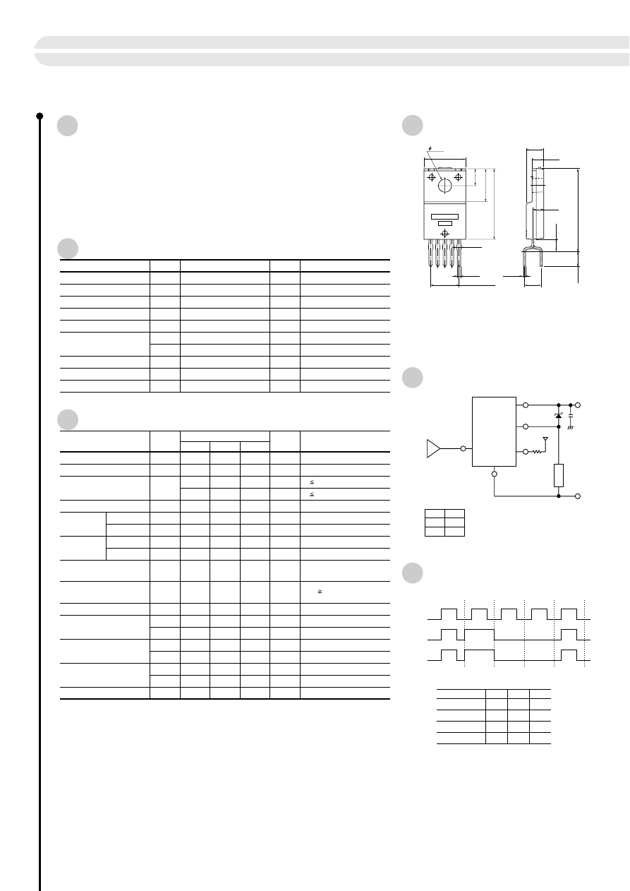
Parameter
Symbol
Unit
Conditions
Ratings
Absolute Maximum Ratings
Electrical Characteristics
Parameter
Symbol
min
typ
max
Unit
Conditions
Ratings
(Ta=25ºC)
Power supply voltage
Input terminal voltage
DIAG terminal voltage
Collector-emitter voltage
Power dissipation
Input voltage
Input current
Operating power supply voltage
Quiescent circuit current
Thermal protection starting
temperature
Open load detection resistor
Output transfer time
DIAG output voltage
DIAG output transfer time
(Ta=25ºC unless otherwise specified)
Saturation voltage of output
transistor
Junction temperature
Operating temperature
Storage temperature
V
B
V
IN
V
DIAG
V
Bopr
V
Bopr
= 14V, V
IN
= 0V
I
O
1.0A, V
Bopr
= 6 to 16V
I
O
2.5A, V
Bopr
= 6 to 16V
V
Bopr
= 6 to 16V
V
Bopr
= 6 to 16V
V
IN
= 5V
V
IN
= 0V
V
Bopr
= 14V, V
O
= V
Bopr
–1.5V
V
Bopr
= 6 to 16V
V
Bopr
6V
V
Bopr
= 14V, I
O
= 1A
V
Bopr
= 14V, I
O
= 1A
V
CC
= 6V, V
Bopr
= 6 to 16V
V
CC
= 6V, V
Bopr
= 6 to 16V, I
DO
= 2mA
V
Bopr
= 14V, I
O
= 1A
V
Bopr
= 14V, I
O
= 1A
V
5
12
6.0
30
mA
0.3
V
0.72
V
V
B
V
0.8
V
1
mA
30
8
30
15
30
6
0.3
30
30
mA
4.5
1
ºC
k
Ω
µ
s
µ
s
V
V
µ
s
µ
s
Iq
Output leak current
V
CEO
= 16V, V
IN
= 0V
2.0
–0.3
–0.1
2
mA
I
O
, leak
V
CE (sat)
V
IH
V
IL
I
IH
I
IL
T
TSD
Overcurrent protection starting
current
2.6
150
A
I
S
Ropen
T
ON
T
OFF
V
DH
V
DL
Minimum load inductance
mH
L
T
PLH
T
PHL
V
CE
P
D1
P
D2
Tj
T
OP
Tstg
Output ON
Output OFF
Output ON
Output OFF
V
V
With infinite heatsink (Tc=25ºC)
Stand-alone without heatsink
V
V
W
W
ºC
ºC
ºC
–13 to +40
–0.3 to V
B
6
40
Output current
I
O
A
2.5
22
1.8
–40 to +150
–40 to +100
–40 to +150
Note:
* The rule of protection against reverse connection of power supply is V
B
= –13V, one minute
(all terminals except, V
B
and GND, are open).
Standard Circuit Diagram
Diagnostic Function
External Dimensions
(unit: mm)
Features
●
Built-in diagnostic function to detect short and open circuiting of loads and
output status signals
●
Low saturation PNP transistor use
●
Allows direct driving using LS-TTL and C-MOS logic levels
●
Built-in overcurrent and thermal protection circuits
●
Built-in protection against reverse connection of power supply
●
Tj = 150ºC guaranteed
●
TO220 equivalent full-mold package not require insulation mica
V
IN
DIAG
V
IN
V
O
DIAG
Normal
Normal
Open load
Overheat
Shorted load
Open load
Normal
Mode
Shorted load
Overheat
L
H
V
O
L
H
L
H
L
H
H
H
H
H
L
H
L
L
L
L
L
H
L
L
L
L
●
DIAG output will be undetermined when a voltage
exceeding 25V is applied to V
B
terminal.
SI-5155S
P
Z
DIAG
5.1k
Ω
GND
1
4
3
5
2
V
IN
V
IN
V
O
H
H
L
L
V
O
V
CC
V
B
Load
LS-TTL
or
CMOS
Truth table
High-side Power Switch ICs
[With Diagnostic Function]
SI-5155S
20
1. GND
2. V
IN
3. V
O
4. DIAG
5. V
B
a: Part No.
b: Lot No.
(Forming No. 1123)
10
2.6
4.2
2.8
3.2
4
7.9
20
max
3.6
16.9
P1.7 • 4 = 6.8
0.94
4
0.85
0.45
+0.2
–0.1
+0.2
–0.1
2.9
R-end
±
0.5
±
0.6
±
0.1
±
0.2
±
0.2
±
0.2
±
0.2
±
0.15
±
0.1
±
0.2
±
0.3
±
0.2
+0.2 –
0.3
a
b
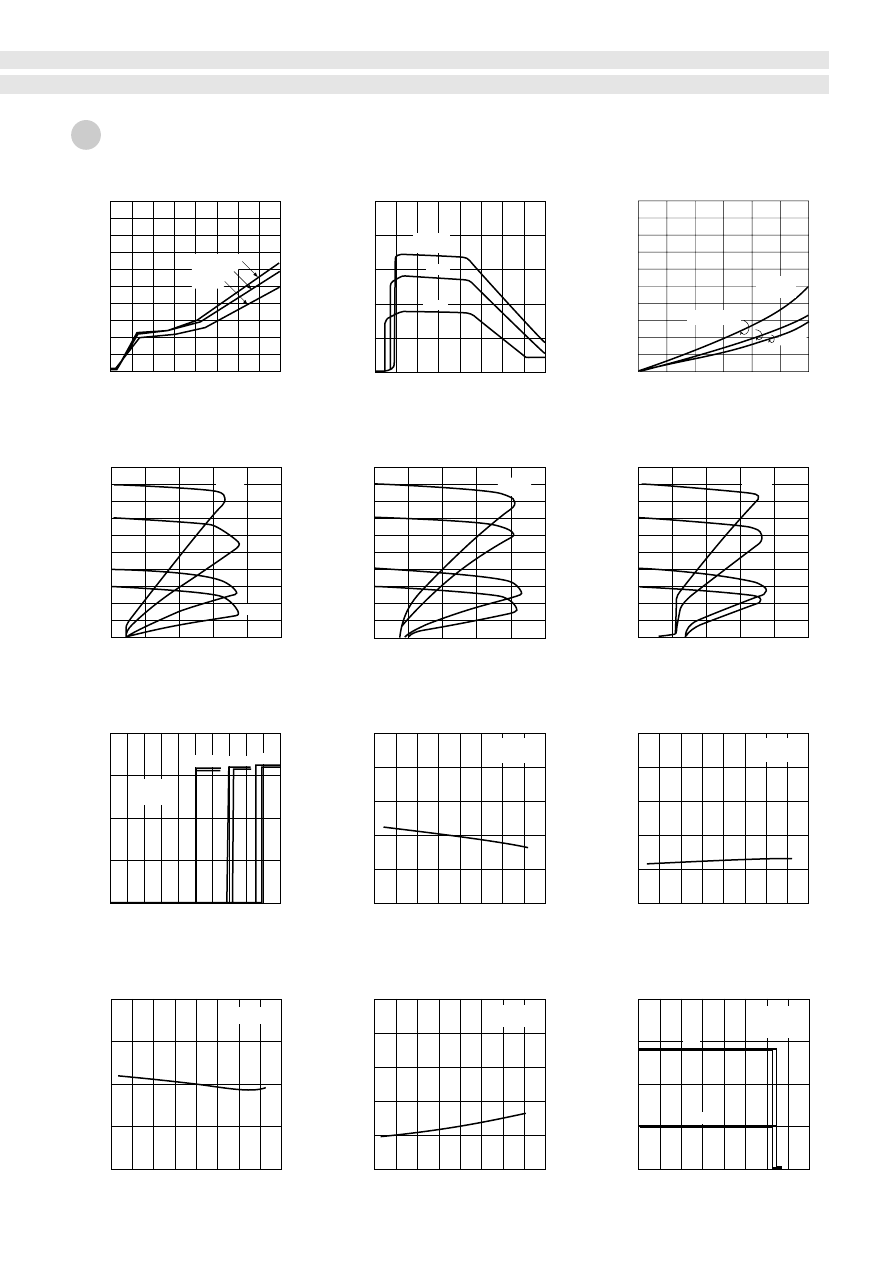
0
10
20
30
0
Iq
(mA)
V
B
(V)
5
10
40
25ºC
150ºC
Ta= –40ºC
0
10
20
30
0
20
50
40
I
B
(mA)
V
B
(V)
30
10
40
–40ºC
25ºC
150ºC
Ta
=
0
1
2
0
2
V
CE
(sat)
(V)
I
O
(A)
1
3
25ºC
V
B
= 6 to 16V
Ta
=
125ºC
0
1
2
0
16
V
O
(V)
I
O
(A)
12
8
4
20
0
16
12
8
4
20
0
16
12
8
4
20
5
4
3
0
1
2
V
O
(V)
I
O
(A)
5
4
3
0
1
2
V
O
(V)
I
O
(A)
5
4
3
14V
8V
14V
8V
14V
8V
6V
0
1
2
0
20
V
O
(V)
V
IN
(th)
(V)
15
10
5
Ta
= 125ºC
–40ºC
25ºC
–50
0
50
100
0
0.8
0.6
1.0
0.4
0.2
I
IH
(mA)
Ta (ºC)
150
–50
0
50
100
0
5
4
3
2
1
I
IL
(
µ
A)
Ta (ºC)
150
–50
0
50
100
0
2
1
I
O leak
(mA)
Ta (ºC)
150
–50
0
50
100
0
0.5
0.4
0.3
0.2
0.1
V
DL
(V)
Ta (ºC)
150
–40ºC
V
B
=
18V
V
B
=
18V
6V
6V
V
B
=
18V
V
B
= 14V
V
IN
= 0V
V
B
= 14V
V
IN
= 5V
V
B
= 16V
I
O
= 1A
V
B
= 14V
V
B
= 14V
I
DIAG
= 2mA
21
0
50
100
0
20
15
10
5
V
O
(V)
Ta (ºC)
200
150
V
O
V
DIAG
V
B
= 14V
V
DIAG
= 5V
I
O
= 10mA
■
Quiescent Circuit Current
■
Circuit Current
■
Saturation Voltage of Output Transistor
■
Overcurrent Protection Characteristics
(Ta=25ºC)
■
Overcurrent Protection Characteristics
(Ta =125ºC)
■
Input Current
(Output OFF)
■
Input Current
(Output ON)
■
Threshold input voltage
■
Overcurrent Protection Characteristics
(Ta = –40ºC)
■
Saturation Voltage of DIAG Output
■
Thermal Protection Characteristics
■
Output Terminal Leak Current
Electrical Characteristics
SI-5155S
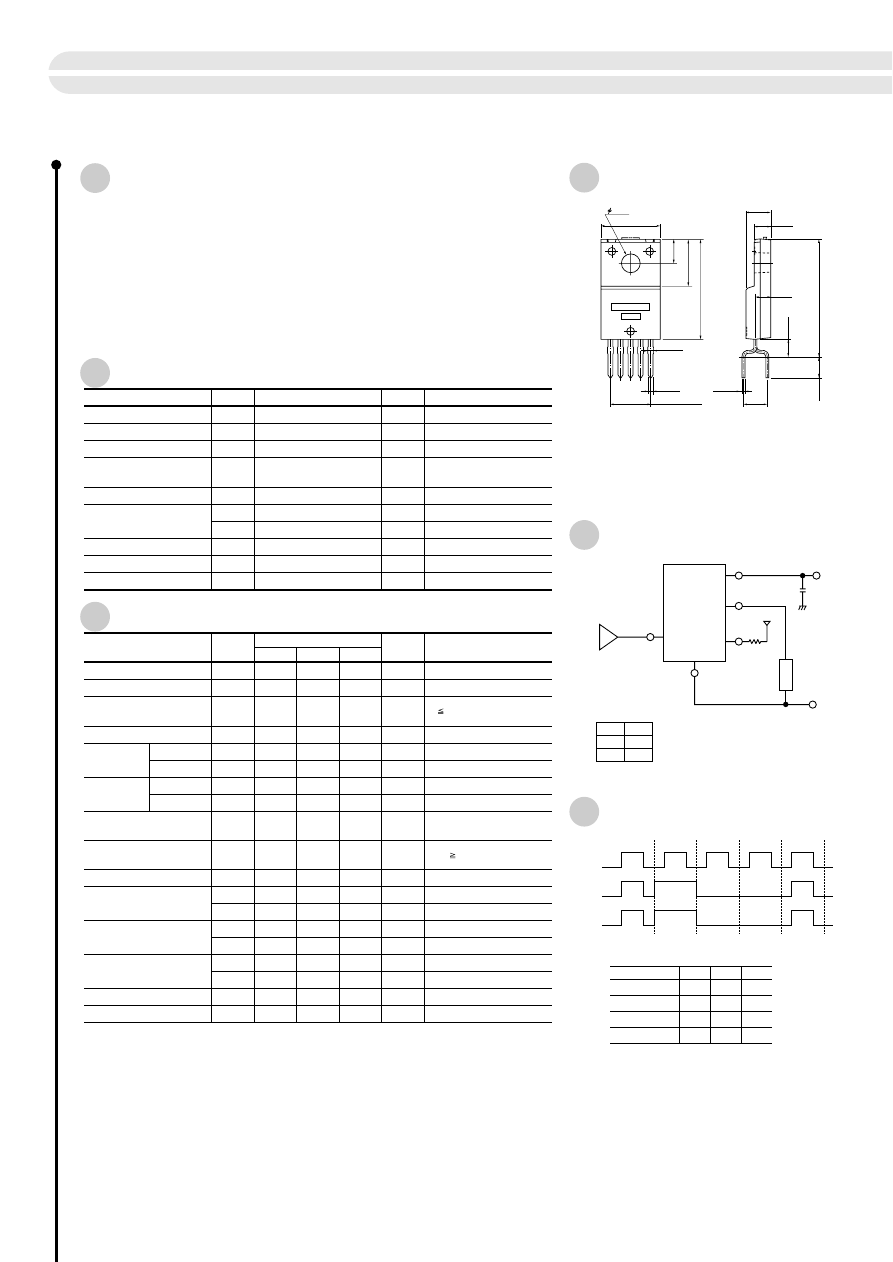
Parameter
Symbol
Unit
Conditions
Ratings
Absolute Maximum Ratings
Electrical Characteristics
Parameter
Symbol
min
typ
max
Unit
Conditions
Ratings
(Ta =25ºC)
Power supply voltage
Input terminal voltage
DIAG terminal voltage
Collector-emitter voltage
Power Dissipation
Input voltage
Input current
Operating power supply voltage
Quiescent circuit current
Thermal protection starting
temperature
Open load detection resistor
Output transfer time
DIAG output voltage
DIAG output transfer time
(Ta=25ºC unless otherwise specified)
Saturation voltage of output
transistor
Junction temperature
Operating temperature
Storage temperature
V
B
V
IN
V
DIAG
V
Bopr
V
Bopr
= 14V, V
IN
= 0V
I
O
2.05A, V
Bopr
= 6 to 16V
V
Bopr
= 6 to 16V
V
Bopr
= 6 to 16V
V
IN
= 5V
V
IN
= 0V
V
Bopr
= 14V, V
O
= V
Bopr
–1.5V
V
Bopr
= 6 to 16V
V
Bopr
6V
V
Bopr
= 14V, I
O
= 1A
V
Bopr
= 14V, I
O
= 1A
V
CC
= 6V, V
Bopr
= 6 to 16V
V
CC
= 6V, V
Bopr
= 6 to 16V, I
DO
= 2mA
V
Bopr
= 14V, I
O
= 1A
V
Bopr
= 14V, I
O
= 1A
I
C
= 5mA
V
5
12
6.0
30
mA
0.47
V
V
B
V
0.8
V
1
mA
30
8
30
15
30
6
0.3
30
30
40
34
28
1
mA
150
4.5
ºC
k
Ω
µ
s
µ
s
V
V
µ
s
µ
s
Iq
Output leak current
V
CEO
= 16V, V
IN
= 0V
2.0
–0.3
–0.1
2
mA
I
O
, leak
V
CE (sat)
V
IH
V
IL
I
IH
I
IL
T
TSD
Overcurrent protection starting
current
2.05
A
I
S
Ropen
T
ON
T
OFF
V
DH
V
DL
Minimum load inductance
mH
L
Surge clamp voltage
V
V
Z
T
PLH
T
PHL
V
CE
P
D1
P
D2
Tj
T
OP
Tstg
Output ON
Output OFF
Output ON
Output OFF
V
V
With infinite heatsink (Tc=25ºC)
Stand-alone without heatsink
Refer to "Surge clamp voltage"
in Electrical Characteristics
V
V
W
W
ºC
ºC
ºC
–13 to +40
–0.3 to V
B
6
V
B
—V
Z
Output current
I
O
A
2.04
22
1.8
–40 to +150
–40 to +100
–40 to +150
Note:
*1. The Zener diode for surge clamping has an energy capability of 140 mJ (single pulse).
* The rule of protection against reverse connection of power supply is V
B
= –13V, one minute.
* This driver is exclusively used for ON/OFF control.
Standard Circuit Diagram
Diagnostic Function
External Dimensions
(unit: mm)
Features
●
Built-in diagnostic function to detect short and open circuiting of loads and
output status signals
●
Low saturation PNP transistor use
●
Allows direct driving using LS-TTL and C-MOS logic levels
●
Built-in overcurrent and thermal protection circuits
●
Built-in protection against reverse connection of power supply
●
Tj = 150ºC guaranteed
●
Built-in Zener diode
●
TO220 equivalent full-mold package not require insulation mica
SI-5153S
DIAG
5.1k
Ω
GND
1
4
3
5
2
V
IN
V
IN
V
O
H
H
L
L
V
O
V
CC
V
IN
DIAG
V
B
Load
LS-TTL
or
CMOS
V
IN
V
O
DIAG
Normal
Normal
Open load
Overheat
Shorted load
Truth table
Open load
Normal
Mode
Shorted load
Overheat
L
H
V
O
L
H
L
H
L
H
H
H
H
H
L
H
L
L
L
L
L
H
L
L
L
L
●
DIAG output will be undetermined when a voltage
exceeding 25V is applied to V
B
terminal.
22
High-side Power Switch ICs
[With Diagnostic Function, Built-in Zener Diode]
SI-5153S
*
1
1. GND
2. V
IN
3. V
O
4. DIAG
5. V
B
a: Part No.
b: Lot No.
(Forming No. 1123)
10
2.6
4.2
2.8
3.2
4
7.9
20
max
3.6
16.9
P1.7 • 4 = 6.8
0.94
4
0.85
0.45
+0.2
–0.1
+0.2
–0.1
2.9
R-end
±
0.5
±
0.6
±
0.1
±
0.2
±
0.2
±
0.2
±
0.2
±
0.15
±
0.1
±
0.2
±
0.3
±
0.2
+0.2 –
0.3
a
b
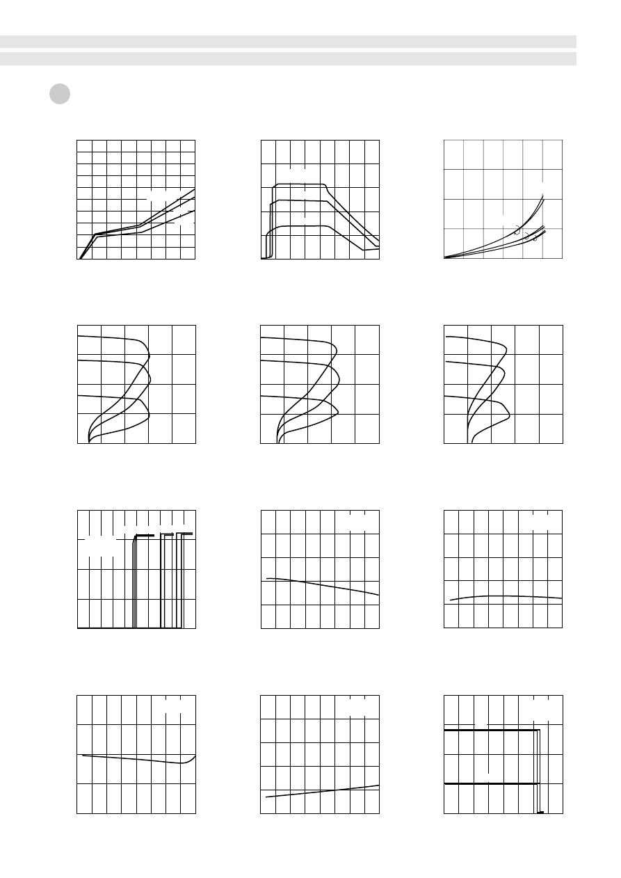
0
10
20
30
0
Iq
(mA)
V
B
(V)
5
10
40
25ºC
150ºC
Ta = –40ºC
0
10
20
30
0
20
50
40
I
B
(mA)
V
B
(V)
30
10
40
–40ºC
25ºC
150ºC
Ta
=
0
1
2
0
2
V
CE
(sat)
(V)
I
O
(A)
1
3
–40ºC
25ºC
V
B
= 6 to 16V
Ta
=
125ºC
0
1
2
0
15
V
O
(V)
I
O
(A)
10
5
20
5
4
3
0
1
2
0
15
V
O
(V)
I
O
(A)
10
5
20
4
5
3
0
1
2
0
15
V
O
(V)
I
O
(A)
10
5
20
4
5
3
14V
8V
V
B
=
18V
14V
8V
V
B
=
18V
14V
8V
V
B
=
18V
0
1
2
0
20
V
O
(V)
V
IN
(th)
(V)
15
10
5
Ta
= 150ºC
–40ºC
25ºC
–50
0
50
100
0
0.8
0.6
1.0
0.4
0.2
I
IH
(mA)
Ta (ºC)
150
–50
0
50
100
0
5
4
3
2
1
I
IL
(
µ
A)
Ta (ºC)
150
–50
0
50
100
0
2
1
I
O leak
(mA)
Ta (ºC)
150
–50
0
50
100
0
0.5
0.4
0.3
0.2
0.1
V
DL
(V)
Ta (ºC)
150
0
50
100
0
20
15
10
5
V
O
(V)
Ta (ºC)
200
150
V
O
V
DIAG
V
B
= 16V
I
O
= 1A
V
B
= 14V
V
IN
= 5V
V
B
= 14V
V
IN
= 0V
V
B
= 14V
V
DIAG
= 5V
I
O
= 10mA
V
B
= 14V
I
DIAG
= 2mA
V
B
= 14V
23
■
Quiescent Circuit Current
■
Circuit Current
■
Saturation Voltage of Output Transistor
■
Overcurrent Protection Characteristics
(Ta = 25ºC)
■
Overcurrent Protection Characteristics
(Ta=125ºC)
■
Input Current
(Output OFF)
■
Input Current
(Output ON)
■
Threshold Characteristics of Input Voltage
■
Overcurrent Protection Characteristics
(Ta= –40ºC)
■
Saturation Voltage of DIAG Output
■
Thermal Protection Characteristics
■
Output Terminal Leak Current
Electrical Characteristics
SI-5153S
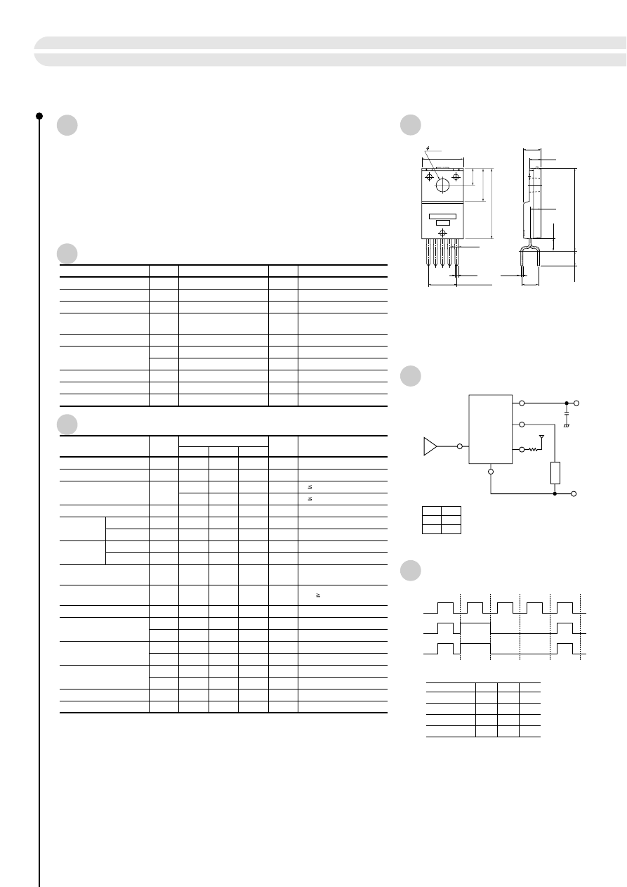
Parameter
Symbol
Unit
Conditions
Ratings
Absolute Maximum Ratings
Electrical Characteristics
Parameter
Symbol
min
typ
max
Unit
Conditions
Ratings
(Ta=25ºC)
Power supply voltage
Input terminal voltage
DIAG terminal voltage
Collector-emitter voltage
Power Dissipation
Input voltage
Input current
Operating power supply voltage
Quiescent circuit current
Thermal protection starting
temperature
Open load detection resistor
Output transfer time
DIAG output voltage
DIAG output transfer time
(Ta=25ºC unless otherwise specified)
Saturation voltage of output
transistor
Junction temperature
Operating temperature
Storage temperature
V
B
V
IN
V
DIAG
V
Bopr
V
Bopr
= 14V, V
IN
= 0V
I
O
1.0A, V
Bopr
= 6 to 16V
V
Bopr
= 6 to 16V
V
Bopr
= 6 to 16V
V
IN
= 5V
V
IN
= 0V
V
Bopr
= 14V, V
O
= V
Bopr
–1.5V
V
Bopr
= 6 to 16V
V
Bopr
6V
V
Bopr
= 14V, I
O
= 1A
V
Bopr
= 14V, I
O
= 1A
V
CC
= 6V, V
Bopr
= 6 to 16V
V
CC
= 6V, V
Bopr
= 6 to 16V, I
DO
= 2mA
V
Bopr
= 14V, I
O
= 1A
V
Bopr
= 14V, I
O
= 1A
I
C
= 5mA
V
5
12
6.0
30
mA
0.3
V
I
O
2.5A, V
Bopr
= 6 to 16V
0.72
V
V
B
V
0.8
V
1
mA
30
8
30
15
30
6
0.3
30
30
40
34
28
1
mA
150
4.5
ºC
k
Ω
µ
s
µ
s
V
V
µ
s
µ
s
Iq
Output leak current
V
CEO
= 16V, V
IN
= 0V
2.0
–0.3
–0.1
2
mA
I
O
, leak
V
CE (sat)
V
IH
V
IL
I
IH
I
IL
T
TSD
Overcurrent protection starting
current
2.6
A
I
S
Ropen
T
ON
T
OFF
V
DH
V
DL
Minimum load inductance
mH
L
Surge clamp voltage
V
V
Z
T
PLH
T
PHL
V
CE
P
D1
P
D2
Tj
T
OP
Tstg
Output ON
Output OFF
Output ON
Output OFF
V
V
With infinite heatsink (Tc =25ºC)
Stand-alone without heatsink
Refer to "Surge clamp voltage" in
Electrical Characteristics
V
V
W
W
ºC
ºC
ºC
–13 to +40
–0.3 to V
B
6
V
B
–V
Z
Output current
I
O
A
2.5
22
1.8
–40 to +150
–40 to +100
–40 to +150
Note:
*1. The Zener diode for surge clamping has an energy capability of 200 mJ (single pulse).
* The rule of protection against reverse connection of power supply is V
B
= –13V, one minute.
* This driver is exclusively used for ON/OFF control.
Standard Circuit Diagram
Diagnostic Function
External Dimensions
(unit: mm)
Features
●
Built-in diagnostic function to detect short and open circuiting of loads and
output status signals
●
Low saturation PNP transistor use
●
Allows direct driving using LS-TTL and C-MOS logic levels
●
Built-in overcurrent and thermal protection circuits
●
Built-in protection against reverse connection of power supply
●
Tj = 150ºC guaranteed
●
Built-in Zener diode
●
TO220 equivalent full-mold package not require insulation mica
V
IN
DIAG
V
IN
V
O
DIAG
Normal
Normal
Open load
Overheat
Shorted load
Open load
Normal
Mode
Shorted load
Overheat
L
H
V
O
L
H
L
H
L
H
H
H
H
H
L
H
L
L
L
L
L
H
L
L
L
L
●
DIAG output will be undetermined when a voltage
exceeding 25V is applied to V
B
terminal.
SI-5154S
DIAG
5.1k
Ω
GND
1
4
3
5
2
V
IN
V
IN
V
O
H
H
L
L
V
O
V
CC
V
B
Load
LS-TTL
or
CMOS
Truth table
24
High-side Power Switch ICs
[With Diagnostic Function, Built-in Zener Diode]
SI-5154S
*
1
1. GND
2. V
IN
3. V
O
4. DIAG
5. V
B
a: Part No.
b: Lot No.
(Forming No. 1123)
10
2.6
4.2
2.8
3.2
4
7.9
20
max
3.6
16.9
P1.7 • 4 = 6.8
0.94
4
0.85
0.45
+0.2
–0.1
+0.2
–0.1
2.9
R-end
±
0.5
±
0.6
±
0.1
±
0.2
±
0.2
±
0.2
±
0.2
±
0.15
±
0.1
±
0.2
±
0.3
±
0.2
+0.2 –
0.3
a
b

0
10
20
30
0
Iq
(mA)
V
B
(V)
5
10
40
25ºC
150ºC
Ta= –40ºC
0
10
20
30
0
20
50
40
I
B
(mA)
V
B
(V)
30
10
40
–40ºC
25ºC
150ºC
Ta
=
0
1
2
0
2
V
CE
(sat)
(V)
I
O
(A)
1
3
25ºC
V
B
= 6 to 16V
Ta
=
125ºC
0
1
2
0
16
V
O
(V)
I
O
(A)
12
8
4
20
0
16
12
8
4
20
0
16
12
8
4
20
5
4
3
0
1
2
V
O
(V)
I
O
(A)
5
4
3
0
1
2
V
O
(V)
I
O
(A)
5
4
3
14V
8V
14V
8V
14V
8V
6V
0
1
2
0
20
V
O
(V)
V
IN
(th)
(V)
15
10
5
Ta
= 125ºC
–40ºC
25ºC
–50
0
50
100
0
0.8
0.6
1.0
0.4
0.2
I
IH
(mA)
Ta (ºC)
150
–50
0
50
100
0
5
4
3
2
1
I
IL
(
µ
A)
Ta (ºC)
150
–50
0
50
100
0
2
1
I
O leak
(mA)
Ta (ºC)
150
–50
0
50
100
0
0.5
0.4
0.3
0.2
0.1
V
DL
(V)
Ta (ºC)
150
–40ºC
V
B
=
18V
V
B
=
18V
6V
6V
V
B
=
18V
V
B
= 14V
V
IN
= 0V
V
B
= 14V
V
IN
= 5V
V
B
= 16V
I
O
= 1A
V
B
= 14V
V
B
= 14V
I
DIAG
= 2mA
25
0
50
100
0
20
15
10
5
V
O
(V)
Ta (ºC)
200
150
V
O
V
DIAG
V
B
= 14V
V
DIAG
= 5V
I
O
= 10mA
■
Quiescent Circuit Current
■
Circuit Current
■
Saturation Voltage of Output Transistor
■
Overcurrent Protection Characteristics
(Ta=25ºC)
■
Overcurrent Protection Characteristics
(Ta=125ºC)
■
Input Current
(Output OFF)
■
Input Current
(Output ON)
■
Threshold input voltage
■
Overcurrent Protection Characteristics
(Ta = –40ºC)
■
Saturation Voltage of DIAG Output
■
Thermal Protection Characteristics
■
Output Terminal Leak Current
Electrical Characteristics
SI-5154S
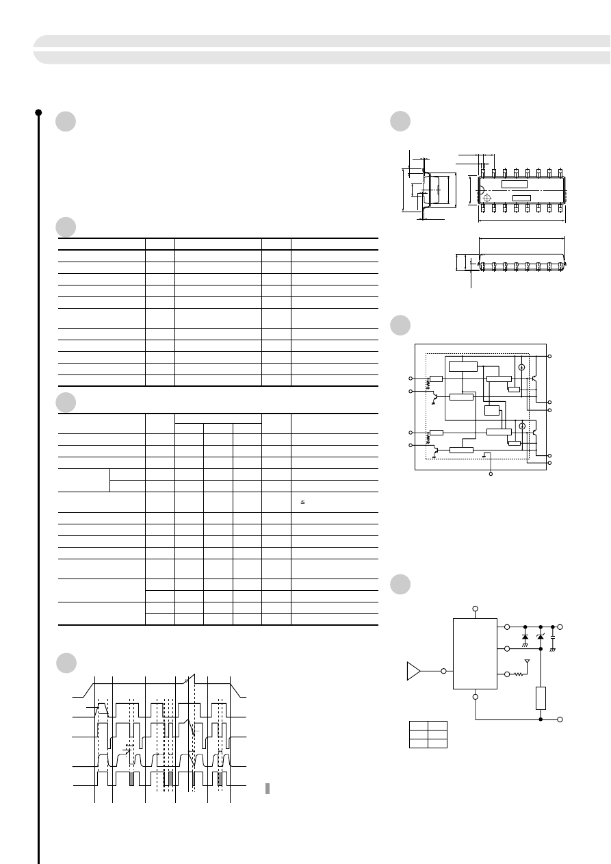
Parameter
Symbol
Unit
Conditions
Ratings
Absolute Maximum Ratings
Electrical Characteristics
Parameter
Symbol
min
typ
max
Unit
Conditions
Ratings
(Ta=25ºC)
Power supply voltage
Input terminal voltage
DIAG output applied voltage
Voltage across power supply
and drive terminal
Power dissipation
Input current
Operating power supply voltage
Quiescent circuit current
Open load detection resistor
Output transfer time
DIAG output transfer time
(V
Bopr
=14V, Ta=25ºC unless otherwise specified)
Junction temperature
Operating temperature
Storage temperature
V
B
V
IN
V
DIAG
V
Bopr
Lo output
V
IN
= 5V
V
IN
= 0V
V
O
= V
Bopr
–1.9V
I
O
= 1A
I
O
= 1A
I
O
= 1A
I
O
= 1A
V
5
12
6.0
0.8
0
16
mA
1.0
100
mA
30
8
30
15
10
15
30
30
30
µ
A
k
Ω
µ
s
µ
s
µ
s
µ
s
Iq
Threshold input voltage
3.0
V
V
IN
th
I
IN
I
IN
Overcurrent protection starting
current
1.6
1
A
I
S
Ropen
Leak current of DIAG output
V
DIAG
= 5V
100
µ
A
I
DGH
Saturation voltage of DIAG output
I
DIAG
= 3mA
0.3
V
V
DL
Saturation voltage of output
transistor
I
O
1.0A, V
Bopr
= 6 to 16V
0.5
V
V
CE (sat)
Output terminal sink current
V
O
= 0V, V
IN
= 0V
2.0
mA
I
O (off)
T
ON
T
OFF
T
PLH
T
PHL
V
B–D
P
D
Tj
T
OP
Tstg
Hi output
Lo output
V
V
Without heatsink, all circuits operating
V
V
W
ºC
ºC
ºC
–13 to +40
–0.3 to +7.0
Drive terminal applied voltage
V
D
V
–0.3 to V
B
–0.3 to +7.0
DIAG output source current
I
DIAG
mA
3
V
B
–0.4
Output current
I
O
A
1.5
2.6
–40 to +150
–40 to +100
–40 to +150
Note: * The rule of protection against reverse connection of power supply is V
B
= –13V, one minute
(all terminals except, V
B
and GND, are open).
Equivalent Circuit Diagram
Standard Circuit Diagram
Diagnostic Function
External Dimensions
(unit: mm)
Features
●
Built-in diagnostic function to detect short and open circuiting of loads and
output status signals
●
Low saturation PNP transistor use
●
Allows direct driving using LS-TTL and C-MOS logic levels
●
Built-in overcurrent protection circuits
●
Built-in protection against reverse connection of power supply
●
Tj = 150ºC guaranteed
●
Surface-mount full-mold package
V
IN
V
O
H
H
L
L
Truth table
SDH04
PZ
D
1
DIAG
5.1k
Ω
GND
IN
Out
V
CC
V
B
Load
Note 1: A pull-down resistor (11 k
Ω
typ.) is connected to the IN terminal.
V
OUT
turns "L" when a high impedance is connected to the IN terminal in
series.
GND
GND
GND
GND
V
B
V
IN
V
OUT
I
O
V
DIAG
Normal
Shorted load
Open load
Overvoltage
Overheat
ERROR SIGNAL for CPU
TSD
OVER
VOLTAGE
OPEN
OPEN
SHORT
Is
3.0V
0.8V
DIAG DET.
DIAG DET.
GND
4,5,13
Drive
Drive
O.C.P
O.C.P
T.S.D
CONT.
11k
Ω
typ.
CONT.
11k
Ω
typ.
Pre. Reg.
IN2
DIAG2
7
6
IN1
2
3
DIAG1
The MIC is bound by the dotted lines.
9,12,16
V
B
Out1
1,15
D1
14
8,10
11
Out2
D2
[Abbreviations]
Drive: Drive circuit
CONT: ON/OFF circuit
Pre.Reg: Pre-regulator
DIAG.DET.: Diagnostic circuit
O.C.P.: Overcurrent protection
T.S.D.: Thermal protection
High-side Power Switch ICs
[Surface-mount 2-circuits]
SDH04
26
a: Part No.
b: Lot No.
a
b
20.0max
2.54
0.89
8.0
6.3
0 to 0.15
3.0
0.25
9.8
1.0
19.56
6.8max
0.75
+0.15
–0.05
+0.15
–0.05
0.3
16
Pin 1
8
9
4.0max
3.6
1.4
SMD-16A
*1. The base terminal (D terminal) is connected to the output
transistor base. It is also connected to the control monolithic
IC. Do not, therefore, apply an external voltage in operation.
*2. SDH04 have two or three terminals of the same function (V
B
,
Out1, Out 2
, GND). The terminals of the same function must be
shorted at a pattern near the product.
*
2
*
2
*
1
*
2
*
2
*
1
±
0.2
±
0.25
±
0.15
±
0.2
±
0.2
±
0.2
±
0.2
±
0.3
±
0.3
±
0.5
0
10
20
30
0
Iq
(mA)
V
B
(V)
10
20
46
40
V
IN
=
0V
V
IN
=
5V
0
10
20
30
0
20
50
40
I
B
(mA)
V
B
(V)
30
10
46
40
–40ºC
25ºC
125ºC
Ta
=
V
IN
=
0V
V
IN
=
5V
0
10
20
30
0
40
100
80
I
B
(mA)
V
B
(V)
60
20
46
40
0
1
2
0
0.5
1.5
V
CE
(sat)
(V)
I
O
(A)
1.0
3
125ºC
25ºC
Ta
=
–40ºC
–40ºC
25ºC
Ta
=
125ºC
V
B
= 16V
V
B
= 6V
0
1
2
0
15
V
O
(V)
I
O
(A)
10
5
20
4
3
0
1
2
0
15
V
O
(V)
V
IN
(V)
10
5
3
V
B
=
14V I
O
=
1A
–40ºC
25ºC
14V
6V
V
B
=
18V
0
1
2
0
15
V
O
(V)
I
O
(A)
10
5
20
4
3
14V
6V
V
B
=
18V
0
1
2
0
15
V
O
(V)
I
O
(A)
10
5
20
4
3
14V
6V
V
B
=
18V
Ta
=
125ºC
0
2
4
6
8
0
1.0
0.8
0.6
0.4
0.2
I
IN
(mA)
V
IN
(V)
10
–50
0
50
100
0
1.0
0.5
I
INL
(
µ
A)
Ta (ºC)
150
V
B
=
14V
V
B
= 14V V
IN
= 0V
–40ºC
25ºC
Ta
=
125ºC
V
O
shorted
V
O
open
V
IN
=
0V
Ta
= –
40ºC
25ºC
125ºC
27
–50
0
50
100
0
0.2
V
DL
(V)
Ta (ºC)
0.1
0.3
150
V
B
=
14V
I
DIAG
=
3mA
■
Quiescent Circuit Current (dual circuit)
■
Circuit Current (single circuit)
■
Circuit Current (dual circuit)
■
Overcurrent Protection Characteristics
(Ta=–40ºC)
■
Overcurrent Protection Characteristics
(Ta=25ºC)
■
Input Terminal Source Current
■
Threshold Characteristics of Input Voltage
■
Overcurrent Protection Characteristics
(Ta=125ºC)
■
Saturation Voltage of Output Transistor
■
Saturation Voltage of DIAG Output
■
Input Terminal Sink Current
Electrical Characteristics
SDH04
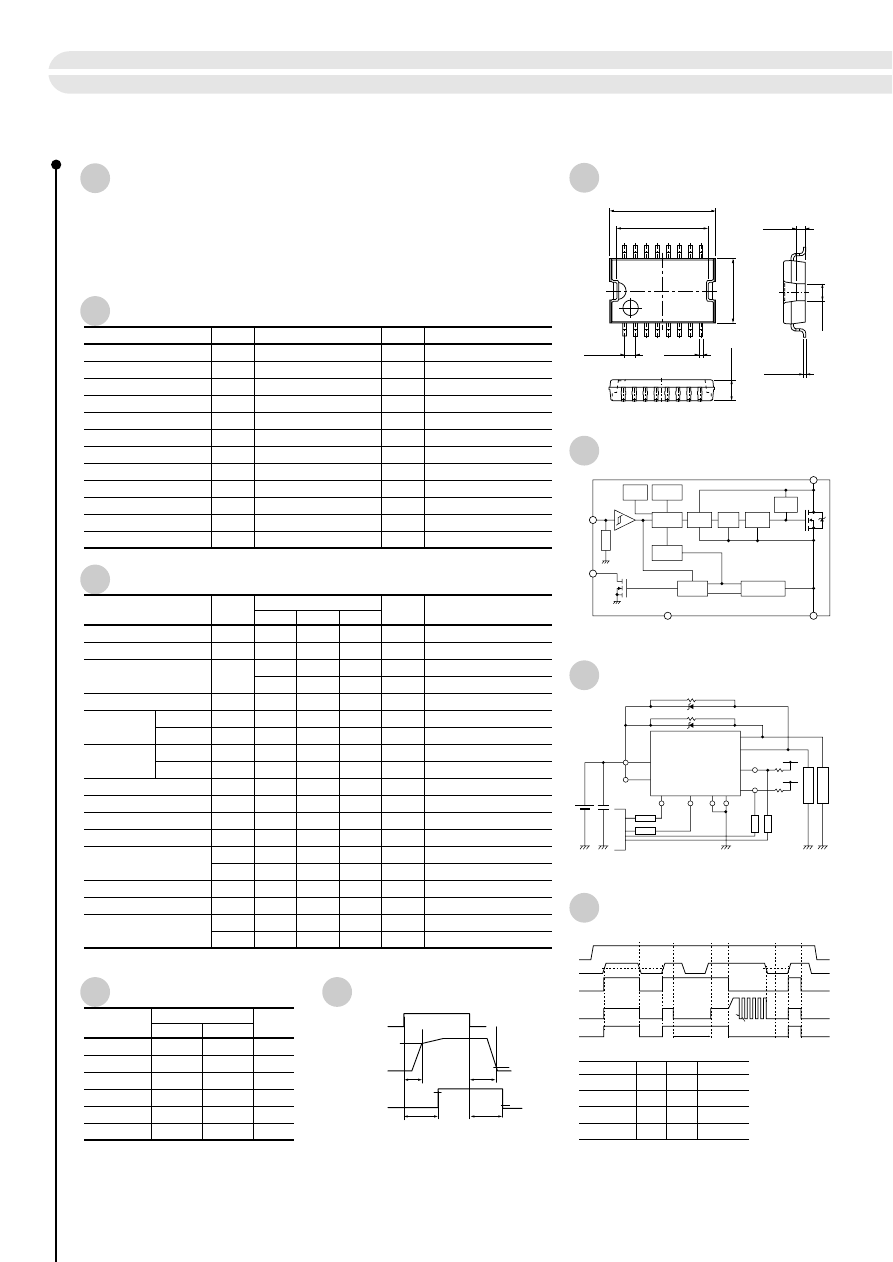
Parameter
Symbol
Unit
Conditions
Ratings
Absolute Maximum Ratings
Electrical Characteristics
Parameter
Symbol
min
typ
max
Unit
Conditions
Ratings
(Ta=25ºC)
Power supply voltage
Input terminal voltage
Input terminal current
DG terminal voltage
Input threshold
voltage
Inpup current
Operating power supply voltage
Quiescent circuit current
Thermal shutdown operating temperature
Load open detection threshold voltage
DG leak current
Low level DG output voltage
Output transfer time
DG output transfer time
(V
B
=14V, Ta=25ºC unless otherwise specified)
Output ON resistance
Channel temperature
Operating temperature
Storage temperature
V
B
V
IN
I
IN
V
B (opr)
V
IN
=0V, V
OUT
=0V
I
O
=1A
I
O
=1A, Ta=80ºC
Ta= –40 to +105ºC
Ta= –40 to +105ºC
V
IN
=5V
V
IN
=0V
V
OUT
=V
O
–1.5V
V
OUT
=0V
R
L
=14
Ω
, V
O
= –5V
R
L
=14
Ω
, V
O
•10%
V
DG
= 5.5V
I
DG
=1.6mA
V
50
2.0
1.8
70
1
5.5
35
mA
200
m
Ω
300
m
Ω
3.0
V
V
200
12
µ
A
165
5
3
4.5
70
3
140
35
0.15
70
45
90
20
0.5
140
120
µ
A
155
1.5
ºC
A
V
µ
s
µ
s
µ
A
V
µ
s
Iq
Output leak current
V
OUT
=0V
1.4
1.0
100
µ
A
I
O
, leak
R
DS (ON)
V
IHth
V
ILth
I
IH
I
IL
T
TSD
Overcurrent protection starting current
Internal current limit
1.9
A
I
S
I
Lim
Vopen
T
ON
T
OFF
V
DGL
I
DG
T
PLH
T
PHL
µ
s
V
DG
V
DS
I
O
P
D
I
F
Tch
T
OP
Tstg
Output ON
Output OFF
Output ON
Output OFF
V
V
Ta=25ºC
mA
V
V
A
W
A
ºC
ºC
ºC
35
–0.3 to 7
5
–0.3 to 7
DG terminal current
Drain to source voltage
Output current
Power dissipation
Source to drain Di forward current
I
DG
mA
5
V
B
–45
1.8
2
0.8
150
–40 to +105
–40 to +150
Parameter
Unit
Ratings
Recommended Operating Conditions (for one channel)
Wave Form
Power supply voltage
V
IH
V
IL
I
O
R
IN
R
DG
5.5
4
–0.3
10
10
16
5.5
0.9
1
20
20
V
V
V
A
k
Ω
k
Ω
Block Diagram (for one channel)
Standard Connection Diagram
Timing Chart
External Dimensions
(unit: mm)
Features
●
Built-in diagnostic function to detect short and open circuiting of loads and
output status signals
●
DMOS 2ch output
●
Allows ON/OFF using C-MOS logic level
●
Built-in overcurrent and thermal protection circuits
V
IN
DG
Open load
Normal
Mode
Shorted load
Overheat
H
L
V
O
H
L
H
L
H
L
H
H
H
H
H
L
L
L
L
L
(Limiting)
H
L
L
L
L
L
Note:
*
1. Transient time is showed Wave Form below.
28
High-side Power Switch ICs
[Surface-mount 2-circuits]
SPF5003
(under development)
*
1
*
1
12.2
±
0.2
1.0
2.5
±
0.2
7.5
±
0.2
10.5
±
0.2
1.27
±
0.25
16
1
8
9
+0.1
–0.05
0.4
+0.15
–0.05
0.25
+0.15
–0.05
2.0
+0.2 –
0.8
Fin
thickness
min
max
IN
DG
V
B
GND
OUT
Thermal
Protect
Input
Logic
Lavel
Shifting
DG
Logic
Open/Short
Sense
Charge
Pump
Current
Limit
Clamp
Chopper
Bias
Vin 1
(7V max)
Vin 2
(7V max)
GND
DG2
DG1
5V
OUT1
OUT2
5V
(10,11)
9
5
R
IN
C
P
U
R
IN
12
4
6
14
15,16
7,8
13
1
SPF5003
V
B
(2, 3)
V
B
V
IN
ON
V
IN
OFF
V
O
open
OCP
TSD
Normal
Normal
Over-
heat
Normal
Normal
Normal
Shorted load
Open load
High inpidance
Internal current limit
TSD
ON
TSD
OFF
V
IN
V
OUT
I
OUT
DG
*
R
IN
and R
DG
are needed to protect CPU and SPF5003 in case of reverse
connection of V
B
terminal.
*
Make V
B
of 1Pin and 9Pin short from the fin to be plated by solder.
R
DG
R
DG
T
ON
V
IN
V
OUT
V
DG
V
DG
• 90%
V
DG
• 10%
V
OUT
• 10%
V
OUT
–5V
T
OFF
T
PLH
T
PHL
Output transfer time
DG output transfer time
Load
Load

29
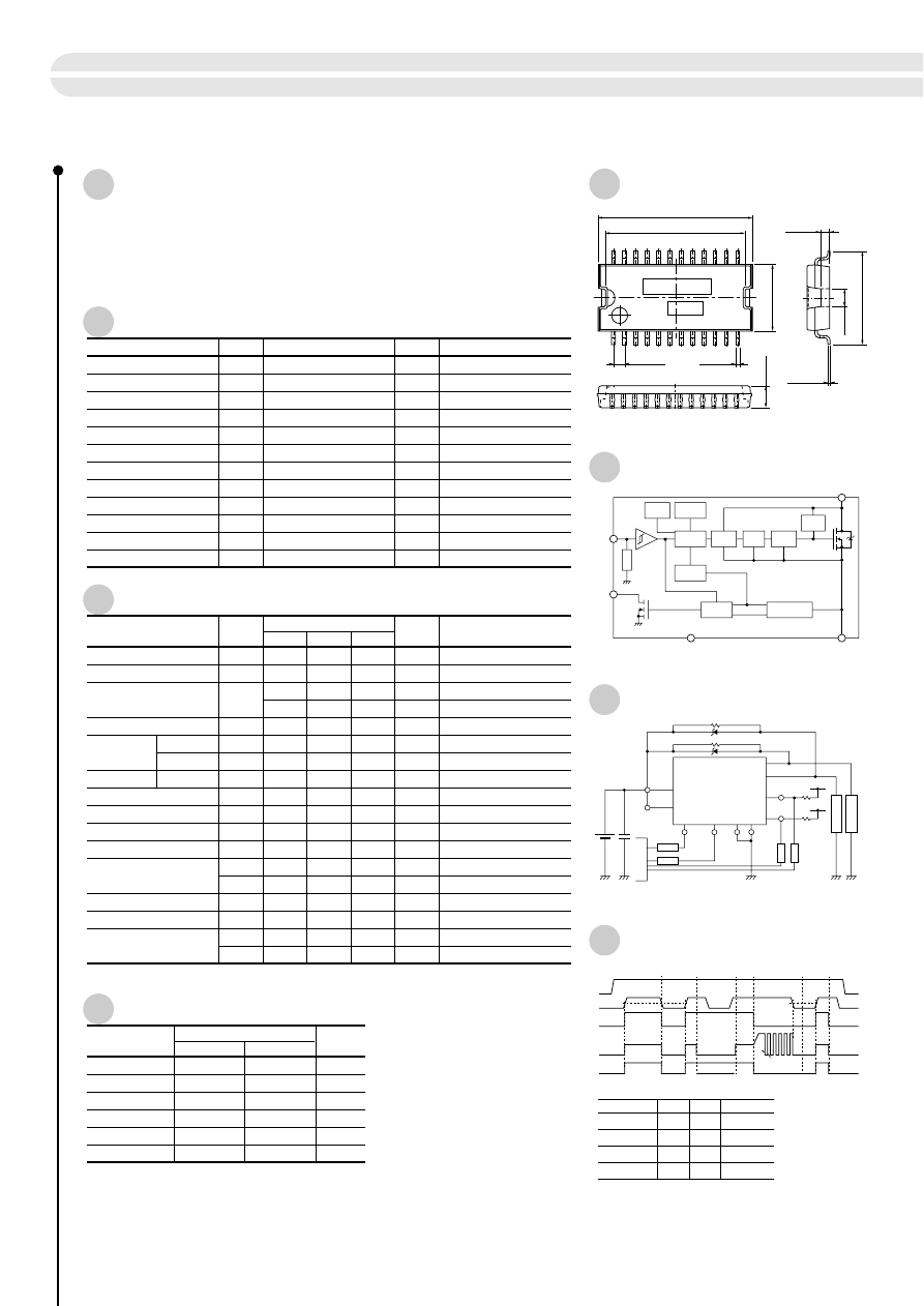
Parameter
Symbol
Unit
Conditions
Ratings
Absolute Maximum Ratings
Electrical Characteristics
Parameter
Symbol
min
typ
max
Unit
Conditions
Ratings
(Ta=25ºC)
Power supply voltage
Input terminal voltage
Input terminal current
DG terminal voltage
Input voltage
Inpup current
Operating power supply voltage
Quiescent circuit current
Thermal shutdown operating temperature
Load open detection threshold voltage
DG leak current
Low level DG output voltage
Output transfer time
DG output transfer time
(V
B
=14V, Ta=25ºC unless otherwise specified)
Output ON resistance
Channel temperature
Operating temperature
Storage temperature
V
B
V
IN
I
IN
V
B (opr)
V
IN
=0V, V
OUT
=0V
I
O
=2A
I
O
=1A, Ta=80ºC
V
IN
=5V
V
OUT
=V
O
–1.5V
V
OUT
=0V
V
DG
=5.5V
I
DG
=1.6mA
V
50
2.0
1.8
70
1
5.5
35
mA
150
m
Ω
250
m
Ω
3.0
V
V
µ
A
165
10
165
3
60
0.15
70
45
20
155
ºC
A
V
µ
s
µ
s
µ
A
V
µ
s
Iq
Output leak current
V
OUT
=0V
Ta= –40 to +105ºC
Ta= –40 to +105ºC
1.0
µ
A
I
O
, leak
R
DS (ON)
V
IH
V
IL
I
IH
T
TSD
Overcurrent protection starting current
Internal current limit
2.6
A
I
S
I
Lim
Vopen
T
ON
T
OFF
V
DGL
I
DG
T
PLH
T
PHL
µ
s
V
DG
V
DS
I
O
P
D
I
F
Tch
T
OP
Tstg
Output ON
Output OFF
Output ON
V
V
Ta=25ºC
mA
V
V
A
W
A
ºC
ºC
ºC
35
–0.3 to 7
5
–0.3 to 7
DG terminal current
Drain to source voltage
Output current
Power dissipation
Source to drain Di forward current
I
DG
mA
5
V
B
–45
2.5
2.7
0.8
150
–40 to +105
–40 to +150
Parameter
Unit
Ratings
Recommended Operating Conditions (for one channel)
Power supply voltage
V
IH
V
IL
I
O
R
IN
R
DG
5.5
4
–0.3
10
10
16
5.5
0.9
1.15
20
20
V
V
V
A
k
Ω
k
Ω
External Dimensions
(unit: mm)
Features
●
Built-in diagnostic function to detect short and open circuiting of loads and
output status signals
●
DMOS 2ch output
●
Allows ON/OFF using C-MOS logic level
●
Built-in overcurrent and thermal protection circuits
30
High-side Power Switch ICs
[Surface-mount 2-circuits]
SPF5004
(under development)
min
max
Block Diagram (for one channel)
Standard Connection Diagram
Timing Chart
IN
DG
V
B
GND
OUT
Thermal
Protect
Input
Logic
Lavel
Shifting
DG
Logic
Open/Short
Sense
Charge
Pump
Current
Limit
Clamp
Chopper
Bias
Vin 1
(7V max)
Vin 2
(7V max)
GND
DG2
DG1
5V
OUT1
OUT2
5V
(16,17,18)
13
23
C
P
U
9
21
24
12
14,15
2,3
11
1
SPF5004
V
B
(4,5,6)
1.0
10.5
±
0.3
+0.1
–0.05
0.25
+0.15
–0.05
2.0
+0.2 –
0.8
Fin
thickness
17.28
±
0.2
2.5
±
0.2
7.5
±
0.2
15.58
±
0.2
1.27
±
0.25
24
1
12
13
0.4
+0.15
–0.05
a
b
a: Part No.
b: Lot No.
*
Make V
B
of 4Pin, 5Pin, 6Pin, 16Pin, 17Pin and 18Pin short from the fin
to be plated by solder.
R
IN
R
IN
R
DG
R
DG
Load
Load
V
B
V
IN
ON
V
IN
OFF
V
O
open
OCP
TSD
Normal
Normal
Over-
heat
Normal
Normal
Normal
Shorted load
Open load
High inpidance
Internal current limit
TSD
ON
TSD
OFF
V
IN
V
OUT
I
OUT
DG
V
IN
DG
Open load
Normal
Mode
Shorted load
Overheat
H
L
V
O
H
L
H
L
H
L
H
H
H
H
H
L
L
L
L
L
(Limiting)
H
L
L
L
L
L

31
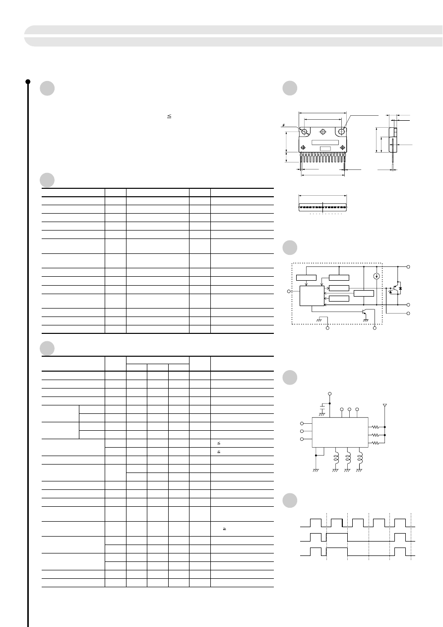
Parameter
Symbol
Unit
Conditions
Ratings
Electrical Characteristics
Absolute Maximum Ratings
Parameter
Symbol
min
typ
max
Unit
Conditions
Ratings
(Ta=25ºC)
Power supply voltage
Input terminal voltage
DIAG output applied voltage
Voltage across power supply
and output terminal
Power Dissipation
Input voltage
Operating power supply voltage
Quiescent circuit current (per circuit)
Thermal protection starting
temperature
Open load detection resistor
Output transfer time
DIAG output transfer time
(V
Bopr
=14V, Tj= –40 to +150ºC unless otherwise specified)
Junction temperature
Operating temperature
Storage temperature
V
B
V
IN
V
DIAG
V
Bopr
Lo output
Tj
= 25ºC
V
O
= V
Bopr
–1.5V
V
Bopr
6V
I
O
= 1A
I
O
= 1A
I
O
= 1A
I
O
= 1A
V
0.8
19.3
1.0
2.5
34
34
1.6
6.0
16
mA
1.5
V
30
100
30
100
60
V
ºC
k
Ω
µ
s
µ
s
µ
s
µ
s
Iq
Circuit current (per circuit)
mA
I
B
0.8
3.7
Threshold input voltage
3.0
V
V
IN
th
V
IN
V
IN
T
TSD
Overcurrent protection starting
current
1.6
5.5
Minimum load inductance
mH
Lo
1.0
Maximum ON duty
%
D
(ON)
0
A
I
S
Ropen
Leak current of DIAG output
V
CC
= 7V
–100
µ
A
I
DGH
Saturation voltage of DIAG output
I
DGH
= –2mA, V
Bopr
= 6 to 16V
0.4
V
V
DL
Saturation voltage of output
transistor
I
O
1.2A, V
Bopr
= 6 to 16V
0.2
V
V
CE (sat)
I
O
1.5A, V
Bopr
= 6 to 16V
V
V
CE (sat)
Output terminal sink current
Tj
= 25ºC, V
CEO
= 14V
5
mA
I
O (off)
Surge clamp voltage
Tj
= 25ºC, I
C
= 10mA
39
V
V
B–O
I
C
= 5mA
40
V
T
ON
T
OFF
T
PLH
T
PHL
V
B–O
P
D
Tj
T
OP
Tstg
Hi output
Lo output
Input current
V
IN
= 5V
V
IN
= 0V
100
29
28
–1.0
mA
µ
A
I
IN
I
IN
Hi output
Lo output
V
V
Stand-alone without heatsink,
all circuits operating
C
= 200pF, R
= 0
Ω
V
V
W
ºC
ºC
ºC
–13 to +40
–0.3 to +7.0
Drive terminal applied voltage
V
D
V
–0.3 to V
B
–0.3 to +7.0
DIAG output source current
I
DIAG
mA
–3
V
B
–34
Voltage across power supply
and drive terminal
V
B–D
V
–0.4
Output current
I
O
A
1.5
Output reverse current
I
O
A
–1.8
Electrostatic resistance
E
S/A
V
±
250
4.8
–40 to +150
–40 to +115
–50 to +150
Note:
* The Zener diode has an energy capability of 200 mJ (single pulse).
* A start failure may occur if a short OFF signal of 10 ms or below is input in the V
IN
terminal.
Equivalent Circuit Diagram
Standard Circuit Diagram
Diagnostic Function
External Dimensions
(unit: mm)
Features
●
Built-in diagnostic function to detect short and open circuiting of loads and
output status signals
●
Low saturation PNP transistor use (V
CE (sat)
0.2V)
●
Allows direct driving using LS-TTL and C-MOS logic levels
●
Built-in Zener diode in transistor eliminates the need of (or simplifies) external
surge absorption circuit
●
Built-in independent overcurrent and thermal protection circuit in each circuit
●
Built-in protection against reverse connection of power supply
●
Tj = 150ºC guaranteed
V
IN
V
O
V
DIAG
Normal
Normal
Open load
Overheat
Shorted load
V
IN
V
B
OUT
D
FLT
GND
MIC
a
c
f
b
d
g
e
SLA2501M
GND
1
OUT
1
OUT
2
OUT
3
FLT
1
IN
1
IN
2
V
B
V
B
V
CC
D
1
D
2
D
3
IN
3
FLT
2
FLT
3
GND
2
5
7
12
6
11
2
10
15
1
3
9
14
4
8
13
a: Part No.
b: Lot No.
31
Ellipse
3.2 • 3.8
14 • P2.03 = (28.42)
24.4
4.8
1.7
2.45
0.65
3.2
12.9
16
9.9
6.4
0.55
1.15
+0.2
–0.1
+0.2
–0.1
+0.2
–0.1
31.3
1 2 3
15
a
b
High-side Power Switch ICs
[3-circuits]
SLA2501M
32
a: Pre-regulator
b: Overvoltage protection circuit
c: Control circuit
d: Driver circuit
e: Overcurrent protection circuit
f: Diagnostic circuit
g: Thermal protection circuit
±
0.1
±
0.2
±
0.2
±
0.15
±
0.2
±
0.2
±
0.2
±
0.2
±
0.5
±
0.2
±
0.1
±
0.2
±
0.15
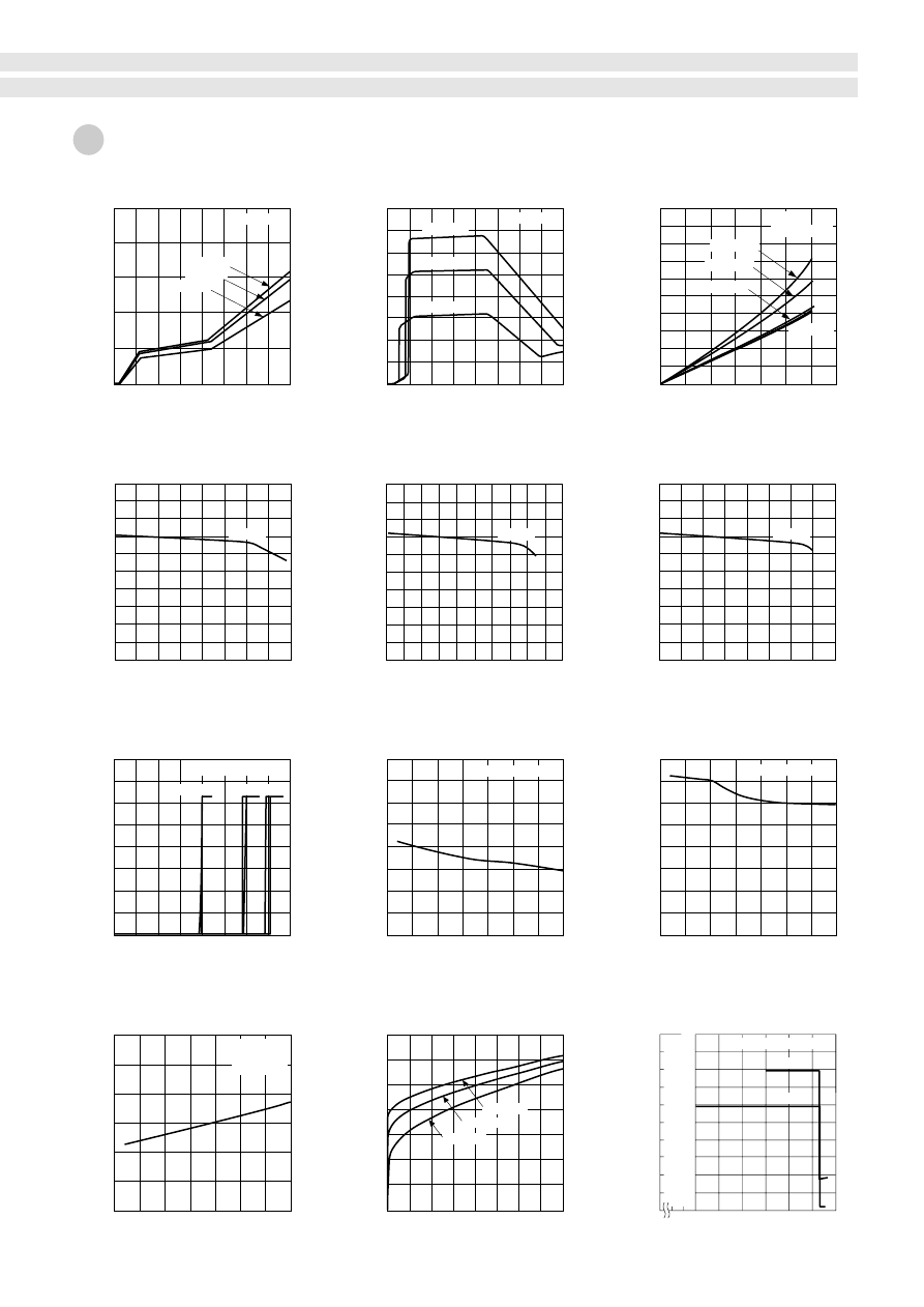
0
10
20
30
0
2
4
Iq (mA)
V
B
(V)
3
1
5
40
=
T –40ºC
a
=
T 25ºC
a
=
T 125ºC
a
=
V 0V
IN
0
10
20
30
0
I
B
(mA)
V
B
(V)
=
T –40ºC
a
40
=
T 25ºC
a
=
T 125ºC
a
10
20
30
40
=
V 5V
IN
0
1
2
3
0
I
O
(A)
3.5
1.0
0.5
V
CE
(sat)
(V)
=
T –40ºC
a
=
T 25ºC
a
=
T 125ºC
a
=
V
B
6 to 16V
=
T 150ºC
a
=
V
IN
5V
0
1
2
0
I
O
(A)
20
10
3
4
5
=
V
B
14V
0
1
2
0
I
O
(A)
20
10
3
4
=
V
B
14V
V
O
(V)
V
O
(V)
0
1
2
0
V
O
(V)
20
10
3
4
=
V
B
14V
I
O
(A)
0
1
2
0
V
O
(V)
V
IN
(V)
=
T 125ºC
a
20
10
3
4
25ºC –40ºC
=
V
B
16V
=
I
1A
OUT
0
--50
1.0
I
IH
(mA)
Ta (ºC)
=
V
B
14V
0.5
0
50
100
125
0V
=
V
IN
0
–50
20
I
IL
(
µ
A)
Ta (ºC)
=
V
B
14V
10
0
50
100
125
0V
=
V
IN
0
–50
0.3
Ta (ºC)
=
V
B
14V
0
50
100
125
5V
=
V
IN
0.2
0.1
V
DL
(V)
3 (mA)
=
I
FLT
Ta (ºC)
=
V
B
16V
0
100
10
FLT
V (V)
10 mA
=
I
O
V
O
(V)
0
60
5
10
20
160
180
O
V
FLT
V
0
I
F
(A)
0
1.4
1.0
V
F
(V)
1
2
3
4
a
T = 125ºC
--
a
T = 40ºC
a
T = 25ºC
1.2
0.2
0.4
0.6
0.8
33
■
Quiescent Circuit Current (single circuit)
■
Circuit Current (single circuit)
■
Saturation Voltage of Output Transistor
■
Overcurrent Protection
Characteristics
(Ta=25ºC)
■
Overcurrent Protection
Characteristics
(Ta=125ºC)
■
Input Current
(Output OFF)
■
Input Current
(Output ON)
■
Threshold Input Voltage
■
Overcurrent Protection
Characteristics
(Ta= –40ºC)
■
Output Reverse Current
■
Thermal Protection
■
Saturation Voltage of DIAG Output
Electrical Characteristics
SLA2501M
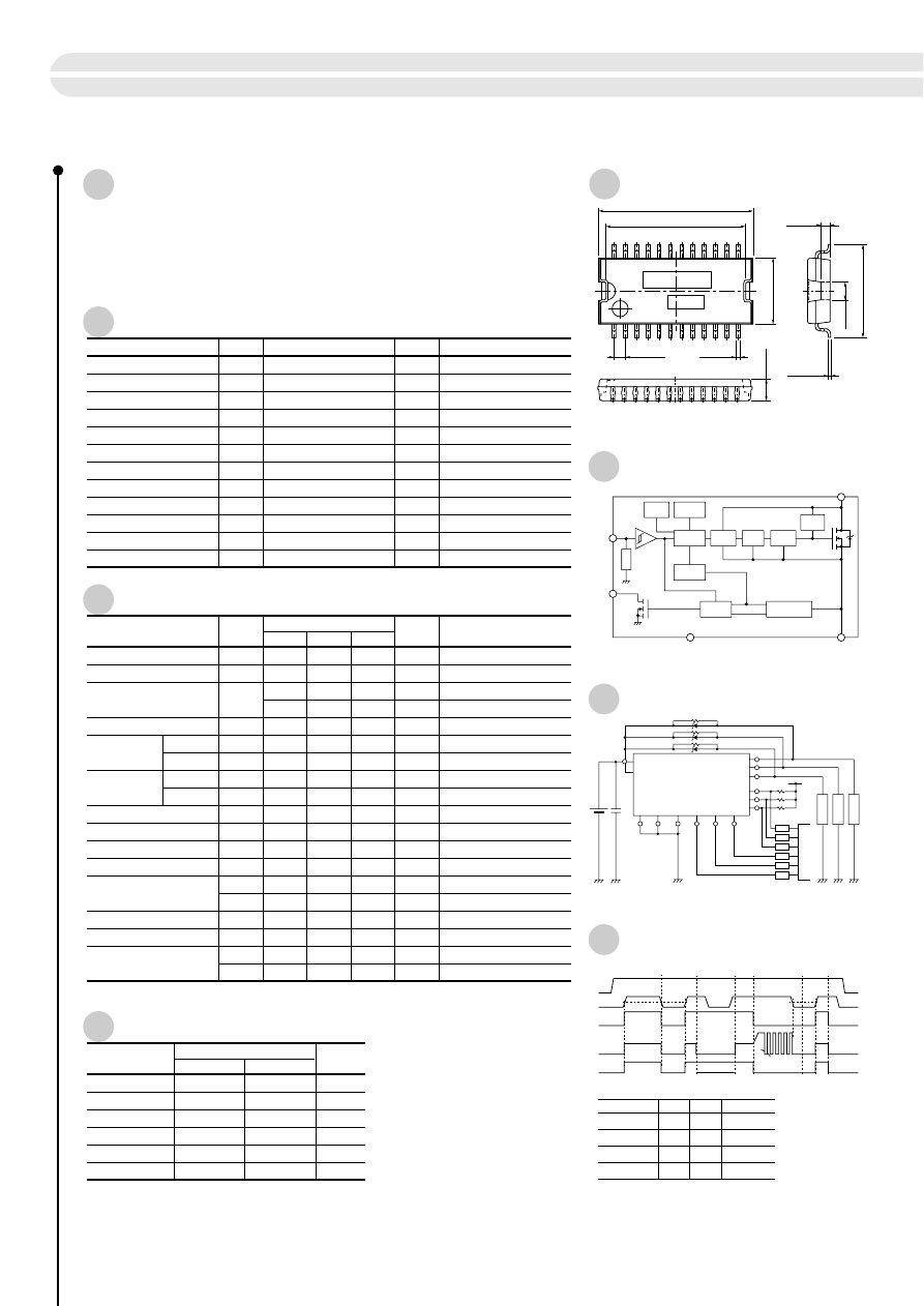
Parameter
Symbol
Unit
Conditions
Ratings
Absolute Maximum Ratings
Electrical Characteristics
Parameter
Symbol
min
typ
max
Unit
Conditions
Ratings
(Ta=25ºC)
Power supply voltage
Input terminal voltage
Input terminal current
DG terminal voltage
Input threshold
voltage
Inpup current
Operating power supply voltage
Quiescent circuit current
Thermal shutdown operating temperature
Load open detection threshold voltage
DG leak current
Low level DG output voltage
Output transfer time
DG output transfer time
(V
B
=14V, Ta=25ºC unless otherwise specified)
Output ON resistance
Channel temperature
Operating temperature
Storage temperature
V
B
V
IN
I
IN
V
B (opr)
V
IN
=0V, V
OUT
=0V
I
O
=1A
I
O
=1A, Ta=80ºC
Ta= –40 to +105ºC
Ta= –40 to +105ºC
V
IN
=5V
V
IN
=0V
V
OUT
=V
O
–1.5V
V
OUT
=0V
R
L
=14
Ω
, V
OUT
=V
B
–5V
R
L
=14
Ω
, V
B
•10%
V
DG
=5.5V
I
DG
=1.6mA
V
50
2.0
1.8
70
1
5.5
35
mA
200
m
Ω
350
m
Ω
3.0
V
V
200
12
µ
A
165
5
3
4.5
70
3
140
35
0.15
70
45
90
20
0.5
140
120
µ
A
155
1.5
ºC
A
V
µ
s
µ
s
µ
A
V
µ
s
Iq
Output leak current
V
OUT
=0V
1.4
1.0
100
µ
A
I
O
, leak
R
DS (ON)
V
IHth
V
ILth
I
IH
I
IL
T
TSD
Overcurrent protection starting current
Internal current limit
1.9
A
I
S
I
Lim
Vopen
T
ON
T
OFF
V
DGL
I
DG
T
PLH
T
PHL
µ
s
V
DG
V
DS
I
O
P
D
I
F
Tch
T
OP
Tstg
Output ON
Output OFF
Output ON
Output OFF
V
V
Ta=25ºC, all circuit operating
mA
V
V
A
W
A
ºC
ºC
ºC
35
–0.3 to 7
5
–0.3 to 7
DG terminal current
Drain to source voltage
Output current
Power dissipation
Source to drain Di forward current
I
DG
mA
5
V
B
–45
1.8
2.7
0.8
150
–40 to +105
–40 to +150
Parameter
Unit
Ratings
Recommended Operating Conditions (for one channel)
Power supply voltage
V
IH
V
IL
I
O
R
IN
R
DG
5.5
4
–0.3
10
10
16
5.5
0.9
1
20
20
V
V
V
A
k
Ω
k
Ω
External Dimensions
(unit: mm)
Features
●
Built-in diagnostic function to detect short and open circuiting of loads and
output status signals
●
DMOS 3ch output
●
Allows ON/OFF using C-MOS logic level
●
Built-in overcurrent and thermal protection circuits
34
High-side Power Switch ICs
[Surface-mount 3-circuits]
SPF5007
(under development)
min
max
Block Diagram (for one channel)
Standard Connection Diagram
Timing Chart
IN
DG
V
B
GND
OUT
Thermal
Protect
Input
Logic
Lavel
Shifting
DG
Logic
Open/Short
Sense
Charge
Pump
Current
Limit
Clamp
Chopper
Bias
IN2
IN3
IN1
GND1
2
13 V
B
1
7
17
18
3
8
5,6
10,11
20,21
4
5V
9
19
GND2
GND3
C
P
U
SPF5007
R
DG
DG1
OUT1
OUT2
OUT3
DG2
DG3
R
DG
R
DG
R
IN
R
IN
R
IN
*
R
IN
and R
DG
are needed to protect CPU and SPF5007 in case of reverse
connection of V
B
terminal.
*
Make V
B
of 1Pin and 13Pin short from the fin to be plated by solder.
1.0
10.5
±
0.3
+0.1
–0.05
0.25
+0.15
–0.05
2.0
+0.2 –
0.8
Fin
thickness
17.28
±
0.2
2.5
±
0.2
7.5
±
0.2
15.58
±
0.2
1.27
±
0.25
24
1
12
13
0.4
+0.15
–0.05
a
b
a: Part No.
b: Lot No.
Load
Load
Load
V
B
V
IN
ON
V
IN
OFF
V
O
open
OCP
TSD
Normal
Normal
Over-
heat
Normal
Normal
Normal
Shorted load
Open load
High inpidance
Internal current limit
TSD
ON
TSD
OFF
V
IN
V
OUT
I
OUT
DG
V
IN
DG
Open load
Normal
Mode
Shorted load
Overheat
H
L
V
O
H
L
H
L
H
L
H
H
H
H
H
L
L
L
L
L
(Limiting)
H
L
L
L
L
L

35
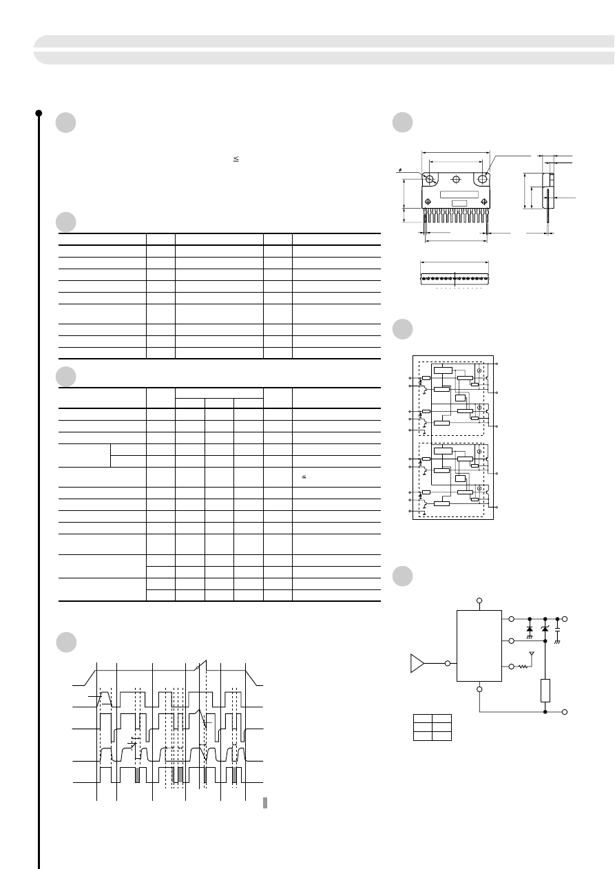
Parameter
Symbol
Unit
Conditions
Ratings
Absolute Maximum Ratings
Electrical Characteristics
Parameter
Symbol
min
typ
max
Unit
Conditions
Ratings
(Ta=25ºC)
Power supply voltage
Input terminal voltage
DIAG output applied voltage
Power Dissipation
Input current
Operating power supply voltage
Quiescent circuit current (per circuit)
Open load detection resistor
Output transfer time
DIAG output transfer time
(V
Bopr
=14V, Ta=25ºC unless otherwise specified)
Junction temperature
Operating temperature
Storage temperature
V
B
V
IN
V
DIAG
V
Bopr
V
IN
= 0V
V
IN
= 5V
V
IN
= 0V
V
O
= V
Bopr
–1.9V
I
O
= 1A
I
O
= 1A
I
O
= 1A
I
O
= 1A
V
5
12
6.0
0.8
0
16
mA
1.0
100
mA
30
8
30
15
10
15
30
30
30
µ
A
k
Ω
µ
s
µ
s
µ
s
µ
s
Iq
Threshold input voltage
3.0
V
V
IN
th
I
IN
I
IN
Overcurrent protection starting
current
1.6
A
I
S
Ropen
Leak current of DIAG output
V
DIAG
= 5V
100
µ
A
I
DGH
Saturation voltage of DIAG output
I
DIAG
= 3mA
0.3
V
V
DL
Saturation voltage of output
transistor
I
O
1.0A, V
Bopr
= 6 to 16V
0.5
V
V
CE (sat)
Output terminal sink current
V
O
= 0V, V
IN
= 0V
2.0
mA
I
O (off)
T
ON
T
OFF
T
PLH
T
PHL
P
D
Tj
T
OP
Tstg
Hi output
Lo output
V
V
Stand-alone operation without
heatsink; all circuits operating
V
W
ºC
ºC
ºC
–13 to +40
–0.3 to +7.0
–0.3 to +7.0
DIAG output source current
I
DIAG
mA
3
Output current
I
O
A
1.2
4.8
–40 to +150
–40 to +100
–50 to +150
Note: * The rule of protection against reverse connection of power supply is V
B
= –13V, one minute
(all terminals except V
B
and GND should be open).
Equivalent Circuit Diagram
Standard Circuit Diagram
Diagnostic Function
External Dimensions
(unit: mm)
Features
●
Built-in diagnostic function to detect short and open circuiting of loads and
output status signals
●
Low saturation PNP transistor use (V
CE (sat)
0.5V)
●
Allows direct driving using LS-TTL and C-MOS logic levels
●
Built-in overcurrent protection circuits
●
Built-in protection against reverse connection of power supply
●
Tj = 150ºC guaranteed
a: Part No.
b: Lot No.
31
Ellipse 3.2 • 3.8
14 • P2.03 = (28.42)
24.4
4.8
1.7
2.45
0.65
3.2
12.9
16
9.9
6.4
0.55
1.15
+0.2
–0.1
+0.2
–0.1
+0.2
–0.1
31.3
1 2 3
15
a
b
V
IN
V
O
H
H
L
L
Truth table
SLA2502M
PZ
D
1
DIAG
5.1k
Ω
GND
IN
Out
V
CC
V
B
Load
GND
GND
GND
GND
V
B
V
IN
V
OUT
I
O
V
DIAG
Normal
Shorted load
Open load
Overvoltage
Overheat
ERROR SIGNAL for CPU
TSD
OVER
VOLTAGE
OPEN
OPEN
SHORT
Is
3.0V
0.8V
NI2
NI1
V
B
Out1
Out2
Pre. Reg.
Drive
Drive
T.S.D
2
3
8
1
7
6
5
4
DIAG1
DIAG2
GND1
DIAG DET
DIAG DET
The MIC is bound by the dotted lines.
11k
Ω
typ.
CONT.
11k
Ω
typ.
CONT.
O.C.P
O.C.P
NI4
NI3
Out3
Out4
Pre. Reg.
Drive
Drive
T.S.D
10
11
9
15
14
13
12
DIAG3
DIAG4
GND4
DIAG DET
DIAG DET
11k
Ω
typ.
CONT.
11k
Ω
typ.
CONT.
O.C.P
O.C.P
SLA2502M
[Abbreviations]
Drive: Drive circuit
CONT: ON/OFF circuit
Pre.Reg: Pre-regulator
DIAG.DET.: Diagnostic circuit
O.C.P.: Overcurrent protection
T.S.D.: Thermal protection
High-side Power Switch ICs
[4-circuits]
SLA2502M
36
Note 1: A pull-down resistor (11k
Ω
typ.) is connected to the IN
terminal. V
OUT
turns "L" when a high impedance is
connected to the IN terminal in series.
Note 2: Grounds GND1 and GND2 are not wired internally. They
must be shorted at a pattern near the product.
±
0.2
±
0.2
±
0.2
±
0.2
±
0.2
±
0.5
±
0.2
±
0.2
±
0.2
±
0.1
±
0.1
±
0.15
±
0.15

0
10
20
30
0
20
50
–40ºC
25ºC
125ºC
V
IN
= 0V
V
B
=
V
IN
= 0V
40
I
B
(mA)
V
B
(V)
30
10
60
46
40
0
1
2
0
15
V
O
(V)
I
O
(A)
10
5
20
3
0
1
2
0
15
V
O
(V)
V
IN
(V)
10
5
20
3
–50
0
50
100
0
0.2
V
DL
(V)
Ta
(ºC)
0.1
0.3
150
0
–50
100
50
0
2
I
IL
(
µ
A)
Ta
(ºC)
1
3
150
0
10
20
30
0
150
I
B
(mA)
V
B
(V)
100
50
200
46
40
0
1
2
0
V
CE
(sat)
(V)
I
O
(A)
0.5
V
B
Ta
=
(V
B
= 14V)
Ta
=
1.0
3
Ta
=
25ºC
125ºC
–40ºC
Ta
=
125ºC
25ºC
–40ºC
18V
14V
6V
V
B
=
V
B
= 14V
V
IN
= 0V
2
1
0
5
4
3
0
0.4
0.3
0.2
0.1
I
IH
(mA)
V
IN
(V)
0.5
6
0
1
2
0
15
V
O
(V)
I
O
(A)
10
5
20
3
18V
14V
6V
V
B
=
0
1
2
0
15
V
O
(V)
I
O
(A)
10
5
20
4
3
18V
14V
6V
125ºC
–40ºC
V
B
= 14V
–40ºC
Ta
=
125ºC
V
B
= 14V
I
DIAG
= 3mA
0
10
20
30
0
Iq
(mA)
V
B
(V)
10
20
46
40
V
O
shorted
V
O
open
V
IN
= 0V
Ta
= –40V
25V
125V
37
■
Circuit Current (single circuit)
■
Circuit Current (4 circuits)
■
Saturation Voltage of Output Transistor
■
Overcurrent Protection Characteristics
(Ta=25ºC)
■
Overcurrent Protection Characteristics
(Ta=125ºC)
■
Input Current
(Output Hi)
■
Input Current
(Output OFF)
■
Threshold Input Voltage
■
Overcurrent Protection Characteristics
(Ta=–40ºC)
■
Quiescent Circuit Current (dual circuit)
■
Saturation Voltage of DIAG Output
25ºC
25ºC
Electrical Characteristics
SLA2502M

0
50
150
100
■
Thermal Protection Characteristics
0
V
O1
(V)
Ta (ºC)
10
5
15
200
5
10
15
■
Open Load Detection Resistor
0
R
OPEN
(k
Ω
)
V
B
(V)
10
5
15
20
5
10
20
15
■
Output Terminal Leak Current (V
O
= 0V)
0.5
I
OLEAK
(mA)
V
B
(V)
1.1
1.0
0.9
0.8
0.7
0.6
25
TSD
V
B
= 14V
RL
= 1.3k
Ω
Ta
=
Ta
=
–40ºC
25ºC
125ºC
125ºC
25ºC
–40ºC
38
High-side Power Switch ICs
[4-circuits]
SLA2502M

39
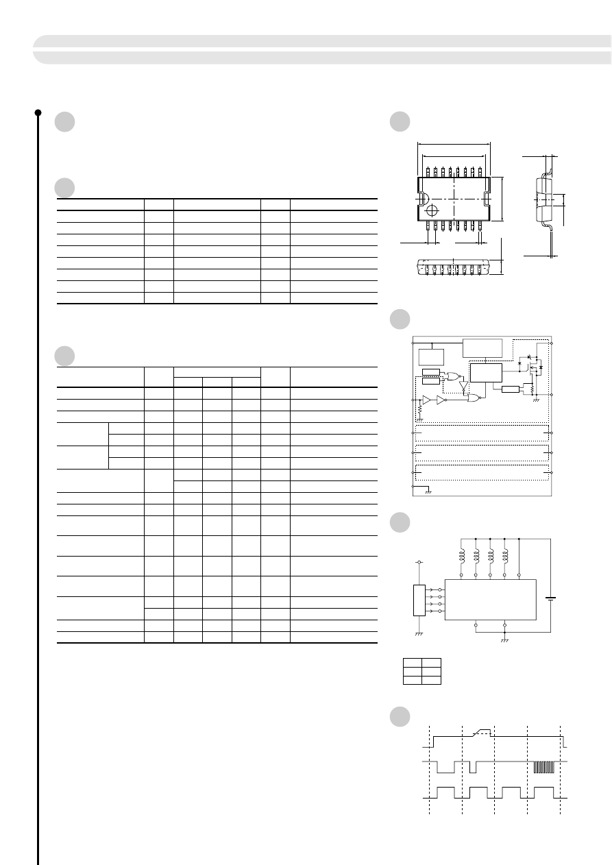
Parameter
Symbol
Unit
Conditions
Ratings
Absolute Maximum Ratings
Electrical Characteristics
Parameter
Symbol
min
typ
max
Unit
Conditions
Ratings
(Ta=25ºC)
Power supply voltage
Input terminal voltage
Power Dissipation
Input voltage
Power supply voltage
Quiescent circuit current
Overcurrent protection starting
current
Forward voltage of output stage
diode
Output transfer time
(V
B
=14V, Ta=25ºC unless otherwise specified)
Storage temperature
Channel temperature
Output avalanche capability
V
B
V
IN
V
Bopr
V
IN
= 0V (all inputs)
I
O
= 1A
R
L
= 14
Ω
, I
O
= 1A
R
L
= 14
Ω
, I
O
= 1A
R
L
= 14
Ω
, I
O
= 1A
R
L
= 14
Ω
, I
O
= 1A
V
5
0.4
0.5
0.6
0.7
50
7
5.5
25
mA
1.5
5.5
V
12
8
10
5
V
A
V
µ
s
µ
s
Iq
Operating circuit current
V
IN
= 5V (all inputs)
8
12
mA
I
CC
3.5
–0.5
V
IN
V
IN
I
S
Thermal protection starting
temperature
151
165
1.1
41
Output rise time
µ
s
T
r
Output fall time
µ
s
T
f
ºC
T
TSD
Overvoltage protection starting
voltage
25
V
V
B (ovp)
V
F
Output leak current
V
O
= 37V
I
F
= 0.5A
10
1.6
40
µ
A
I
OH
Output clamp voltage
I
O
= 1A
55
V
V
OUT (clamp)
Output ON resistance
30
Ω
R
DS (ON)
V
B
= 5.5V
Ω
T
ON
T
OFF
P
D
Tstg
Tch
E
AV
Hi output
Lo output
Input current
V
IN
= 5V
V
IN
= 0V
50
µ
A
µ
A
I
IN
I
IN
Hi output
Lo output
V
V
W
ºC
ºC
mJ
Single pulse
40
–0.5 to +7.5
Output terminal voltage
V
OUT
V
37
Output current
I
O
A
1.8
2
–40 to +150
150
50
Equivalent Circuit Diagram
Circuit Example
Timing Chart
External Dimensions
(unit: mm)
Features
●
DMOS 4ch output
●
Allows ON/OFF using C-MOS logic level
●
Built-in overcurrent, overvoltage and thermal protection circuits
Low-side Switch ICs
[Surface-mount 4-circuits]
SPF5002A
40
12.2
1.0
2.5
7.5
10.5
1.27
16
1
8
9
0.4
+0.15
–0.05
+0.1
–0.05
+0.15
–0.05
+0.2 –
0.8
0.25
2.0
Fin
thickness
V
B
V
OUT
1
V
IN
1
V
IN
2
V
IN
3
V
IN
4
V
OUT
2
V
OUT
3
V
OUT
4
L-GND
P-GND
Reg. REF
OVP
TSD
250 k
Ω
typ
Gate Protction
Gate Driver
OCP
Use L-GND and P-GND being connected.
V
B
V
OUT
V
IN
OVP
Normal
Overvoltage
Overheat
Overcurrent
* Self-excited frequency is used in the overcurrent protection.
V
IN
V
O
H
L
L
H
Truth table
±
0.2
±
0.25
±
0.2
±
0.2
±
0.2
V
CC
V
B
4
6
12
14
IN1
OUT1 OUT3
OUT2 OUT4
IN2
IN3
IN4
L-GND
P-GND
CONTROL
UNIT
13
1,9
SPF5002A
2
10
7
15
5
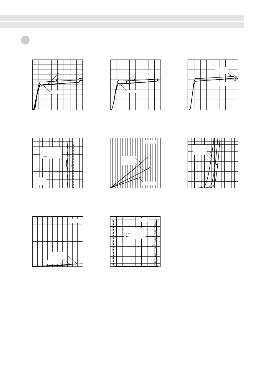
41
■
Quiescent Circuit Current
0
10
20
30
40
0
4
8
Iq (mA)
V
B
(V)
6
2
10
0
4
8
6
2
10
0
4
8
6
2
10
■
Circuit Current (single circuit)
0
10
20
30
40
Id (mA)
V
B
(V)
■
Threshold Input Voltage
0
1
2
3
0
5
10
V
O
(V)
V
IN (th)
(V)
15
■
Overcurrent Protection Characteristics
0
1.0
2.0
0
V
O
(V)
I
O
(A)
10
5
15
■
Forward Voltage of Output Stage Diode
0
0.5
1.0
1.5
0
0.5
1.5
I
F
(A)
V
F
(V)
1.0
■
Output ON Voltage
0
0.5
1.0
1.5
2.0
0
0.4
0.8
V
DS (ON)
(V)
I
O
(A)
0.6
0.2
1.0
■
Circuit Current (4 circuits)
10
20
30
40
Id (mA)
V
B
(V)
■
Overvoltage Protection Starting Voltage
0
10
20
30
40
0
V
O
(V)
V
B
(V)
10
5
15
Ta
= 120ºC
Ta
= 25ºC
Ta
= –40ºC
Ta
= 125ºC
Ta
= 25ºC
Ta
= –40ºC
Ta
= 25ºC
Ta
= –40ºC
Ta
= 125ºC
V
O
= 14V
I
O
= 0.1A
Ta
= –40ºC
Ta
= 125ºC
Ta
= 25ºC
V
B
= 14V
Ta
= 125ºC
Ta
= 25ºC
Ta
= –40ºC
V
B
=14V
Ta
= 120ºC
Ta
= 25ºC
Ta
= –40ºC
I
O
= 0.1A
Ta
= –40ºC
Ta
= 25ºC
Ta
= 125ºC
Electrical Characteristics
Ta
= –40ºC
Ta
= 25ºC
Ta
= 125ºC
SPF5002A
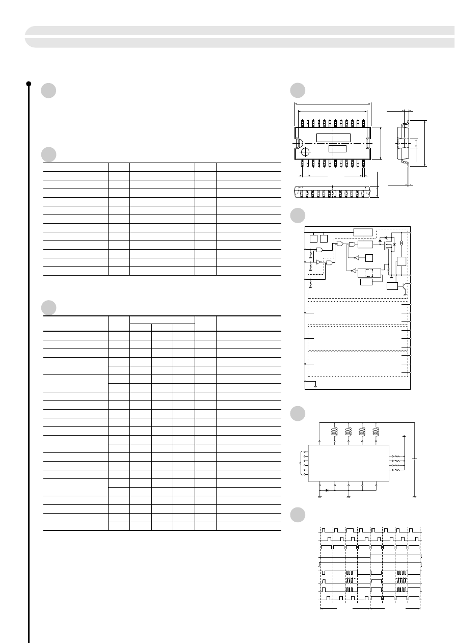
Parameter
Symbol
Unit
Conditions
Ratings
Absolute Maximum Ratings
(Ta=25ºC)
Power supply voltage
Power Dissipation
Storage temperature
Channel temperature
Output avalanche capability
V
B
P
D
Tstg
Tch
E
AV
V
W
ºC
ºC
mJ
Single pulse
40
Input terminal voltage
V
( IN, SEL, B/U)
V
–0.5 to +6.5
Output terminal voltage (DC)
V
OUT
V
50
Output terminal voltage (pulse)
V
OUT
V
Output clamping (max 70V)
Output current (DC)
I
OUT
A
±
2.9
Output current (pulse)
I
OUT
A
Over current protection starting current
Diag output source current
V
DIAG
V
6.5
Diag output voltage
I
DIAG
mA
5
2.8
–40 to +150
150
80
Equivalent Circuit Diagram
Circuit Example
Timing Chart
External Dimensions
(unit: mm)
Features
●
DMOS 4ch output
●
Allows ON/OFF using C-MOS logic level
●
Built-in over current and thermal protection circuit and diagnostic function to
detect open load
●
Built-in output status signals (over current, over heat and open load)
42
V
B
(7)
V
IN
B/U
(17)
V
IN
SEL
(5)
V
IN
1
(6)
V
IN
2
(8)
V
IN
3
(18)
V
IN
4
(20)
L-GND
(19)
V
OUT
1
(4)
V
OUT
2
(9)
V
DIAG
1
(3)
V
OUT
SENSE
V
DIAG
2
(10)
P-GND1
(1, 2)
P-GND2
(11, 12)
V
OUT
3
(16)
V
DIAG
3
(15)
P-GND3
(13, 14)
V
OUT
4
(21)
V
DIAG
4
(22)
P-GND4
(23, 24)
Reg
Ref
Gate Protection
Gate driver
TSD
OUT OCP
Latch
Set
Reset
OSC
Monitor
V
B
7
6
3
10
15
22
8
18
20
17
19
1, 2
11, 12
13, 14
23, 24
5
4
9
16
21
LG
PG1
PG2
PG3
PG4
V
IN
1
V
IN
2
V
IN
3
V
IN
4
V
IN
B/U
V
IN
SEL
OUT1
OUT2
OUT3
OUT4
DIAG1
DIAG2
DIAG3
DIAG4
SPF5009
Main input signal 1
V
IN
1
Main input signal 2
V
IN
2
Backup input signal
V
IN
B/U
Input select signal
V
IN
SEL
Power supply voltage
V
B
Output voltage 1
V
OUT
1
Output current 1
I
OUT
1
DIAG output 1
V
DIAG
1
DIAG output 2
V
DIAG
2
Nomal
Nomal
Main mode
Backup mode
Output 1
Overheat
Output 1
Overheat
Output 1
Over current
Output 1
Open load
Output 1
Over current
Output 1
Open load
OCP
OCP
Electrical Characteristics
Parameter
Symbol
min
typ
max
Unit
Conditions
Ratings
Quiescent circuit current
Operating circuit current
Overcurrent protection starting current
Forward voltage of output stage diode
Output moniter threshold voltage
(V
B
=14V, Ta
= 25ºC unless otherwise specified)
I
q
V
B
=14V, V
IN
=0V
V
B
=14V, V
O
=1A
V
B
=14V
V
B
=14V, R
L
=14
Ω
, I
O
=1A
V
B
=14V, R
L
=14
Ω
, I
O
=1A
V
B
=14V, R
L
=14
Ω
, I
O
=1A
V
B
=14V, R
L
=14
Ω
, I
O
=1A
V
B
=14V, R
L
=14
Ω
, I
O
=1A
V
B
=14V, R
L
=14
Ω
, I
O
=1A
9
65
15
12
Power supply voltage
V
B (opr)
V
5.5
40
mA
200
1.5
V
12
8
10
5
V
V
V
V
µ
s
µ
s
I
d
Input voltage
(1 to 4, SEL, B/U)
Input current (single circuit)
(1 to 4, SEL, B/U)
V
B
=14V, V
IN
=5V (all inputs)
12
6.5
mA
V
IN (H)
3.5
–0.5
V
IN (L)
I
IN (H)
I
S
Thermal shutdown operating temperature
151
165
60
Output rise time
Output fall time
Output transfer time
µ
s
T
r
µ
s
T
f
12
DIAG output transfer time
t
DON
8
µ
s
µ
s
t
DOFF
ºC
T
TSD
3.0
A
DIAG output voltage
6.4
V
V
DIAG (L)
V
DIAG (H)
V
t h
M
Output leak current
I
F
=1A
0.5
10
DIAG output leak current
µ
A
I
DH
I
OH
V
F
Output clamp voltage
Output ON resistance
V
B
=14V, I
O
=1A
V
B
=14V, V
O
=50V
70
50
1.5
2
6.5
V
V
OUT (clamp)
V
B
=14V, I
O
=1A
0.18
Ω
T
ON
T
OFF
V
B
=14V, V
IN
=0V
V
B
=14V, V
IN
=5V
V
B
=14V
V
B
=14V, V
DIAG
=6.5V
V
B
=14V, I
DIAG
=5mA
V
B
=14V, V
DIAG
=6.5V
V
B
=14V
V
B
=14V
30
µ
A
µ
A
µ
A
I
IN (L)
R
DS (ON)
1.0
10.5
±
0.3
+0.1
–0.05
0.25
+0.15
–0.05
2.0
+0.2 –
0.8
17.28
±
0.2
2.5
±
0.2
7.5
±
0.2
15.58
±
0.2
1.27
±
0.25
24
1
12
13
0.4
+0.15
–0.05
a
b
a : Part No.
b: Lot No.
Fin
thickness
Low-side Switch ICs
[Surface-mount 4-circuits]
SPF5009
(under development)

43
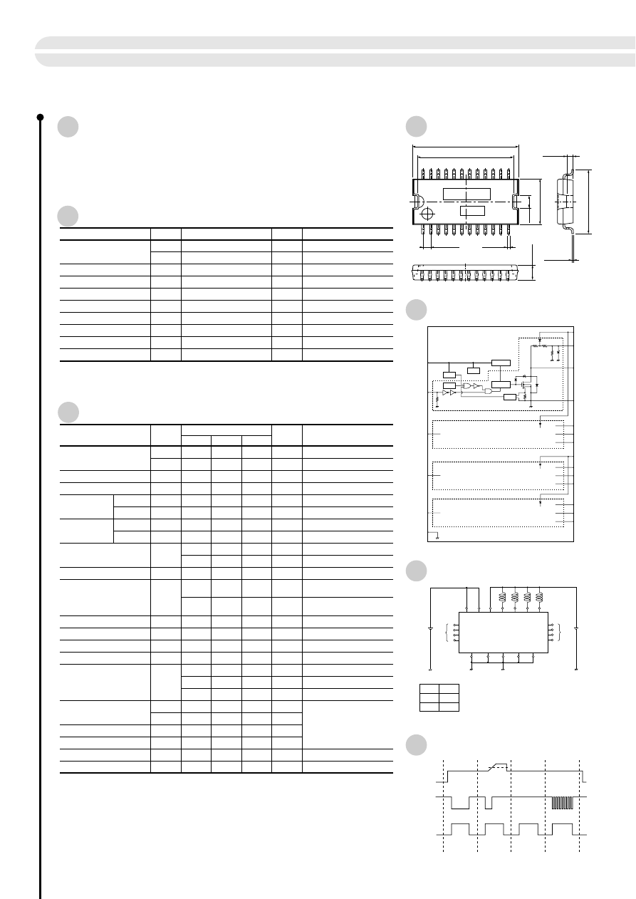
Parameter
Symbol
Unit
Conditions
Ratings
Absolute Maximum Ratings
Electrical Characteristics
Parameter
Symbol
min
typ
max
Unit
Conditions
Ratings
(Ta=25ºC)
DC input voltage
Logic input voltage
Power Dissipation
Input voltage
Quiescent circuit current
Overcurrent protection
operating current
Forward voltage of output stage diode
Output transfer time
(V
B
=14V, Ta
= 25ºC unless otherwise specified)
Storage temperature
Channel temperature
Output avalanche capability
V
B
V
IN
V
CC (opr)
V
B
=14V, V
IN
=0V
V
B
=14V, V
O
=1A
V
B
=14V
V
B
=14V, R
L
=14
Ω
, I
O
=1A
V
4
50
6
4.5
5.5
Power supply voltage
V
B (opr)
V
5.5
40
mA
1.5
5.5
V
12
8
10
5
V
A
V
µ
s
µ
s
Iq
Operating circuit current
V
B
=14V, V
IN
=5V
8
12
mA
Id
3.5
–0.5
V
IN
V
IN
I
S
Thermal shutdown operating temperature
151
165
0.2
8
6
A
5
0.195
45
Output rise time
µ
s
T
r
Output fall time
µ
s
T
f
0.205
Output-diag voltage ratio
r
a (DIAG)
V
B
=14V, V
CC
=5V, V
O
=40V
V
B
=14V, V
O
=1 to 14V, Rdiag=500k
Ω
4.85
Diag output clamping voltage
V
V
DIAG (clamp)
ºC
T
TSD
6
A
Overvoltage protection starting voltage
25
V
V
B (ovp)
V
F
Output leak current
V
B
=14V, V
CC
=5V, V
IN
=0V,
V
O
=40V, Ta=25ºC
V
B
=14V, V
CC
=5V, V
IN
=0V,
V
O
=14V, Ta=25ºC
I
F
=1A
2.8
1.6
40
Overvoltage protection hysteresis voltage
V
V
B (ovp•hys)
mA
I
O
H
900
µ
A
Output clamp voltage
V
B
=14V, I
O
=1A
55
V
V
OUT (clamp)
Output ON resistance
V
B
=14V, I
O
=1A, Ta=125ºC
0.3
–30
Ω
R
DS (ON)
V
B
=14V, I
O
=1A, Ta=25ºC
0.2
Ω
T
ON
T
OFF
P
D
Tstg
Tch
E
AV
Hi output
Lo output
Input current
V
B
=14V, V
IN
=5V
V
B
=14V, I
O
1A
V
B
=14V
V
B
=14V, Ta=–40ºC
V
B
=14V, Ta=25ºC
V
B
=14V, Ta=125ºC
50
µ
A
µ
A
I
IN
I
IN
Hi output
Lo output
V
V
W
ºC
ºC
mJ
Single pulse
40
–0.5 to +7.5
Output voltage
V
O
V
40 (DC)
Output current
I
O
A
Self Limited
V
CC
V
7.5
Diag output voltage
V
DIAG
V
0 to V
CC
2.8 to 5
–40 to +150
150
100
Equivalent Circuit Diagram
Circuit Example
Timing Chart
External Dimensions
(unit: mm)
Features
●
Output monitor circuit (DIAG)
●
DMOS 4ch output
●
Allows ON/OFF using C-MOS logic level
●
Built-in overcurrent, overvoltage and thermal protection circuits
Low-side Switch ICs
[Surface-mount 4-circuits with Output Monitor]
SPF5012
(under development)
44
V
IN
V
O
H
L
L
H
Truth table
V
IN
1
V
IN
2
V
CC
1-2 V
CC
3-4
V
OUT
1 V
OUT
2 V
OUT
3 V
OUT
4
V
B
V
CC
V
IN
3
V
IN
4
L-GND
6
7
18
19
3
10
15
22
5
8
17
20
16
21
4
9
11,12
13,14
23,24
1, 2
P-GND1 P-GND2
Diag1
Diag2
Diag3
Diag4
P-GND3 P-GND4
SPF5012
Input
signal
Diag
output
V
B
(19)
V
IN
1
(4)
V
IN
2
(9)
V
IN
3
(16)
V
IN
4
(21)
L. GND
(6)
V
CC
1-2
(7)
V
CC
3-4
(18)
Diag1
(5)
Diag2
(8)
Diag3
(17)
Diag4
(20)
V
OUT
1
(3)
V
OUT
2
(10)
V
OUT
3
(15)
V
OUT
4
(22)
P. GND1
(1, 2)
P. GND2
(11, 12)
P. GND3
(13, 14)
P. GND4
(23, 24)
Gate Protection
Reg
OVP
OCP
TSD
Ch1
Ch2
Ch3
Ch4
Gate driver
*
1. At the clamping operation, refer to the section of V
OUT (clamp)
in electrical characteristics
*
2. Changes by the patern of mounted substrate
*
1
*
2
1.0
10.5
±
0.3
+0.1
–0.05
0.25
+0.15
–0.05
2.5
±
0.2
17.28
±
0.2
7.5
±
0.2
2
±
0.2
15.58
±
0.2
1.27
±
0.25
24
1
12
13
0.4
+0.15
–0.05
a
b
a : Part No.
b: Lot No.
Fin
thickness
V
B
V
OUT
V
IN
OVP
Normal
Overvoltage
Overheat
Overcurrent
* Self-excited frequency is used in the overcurrent protection.

45
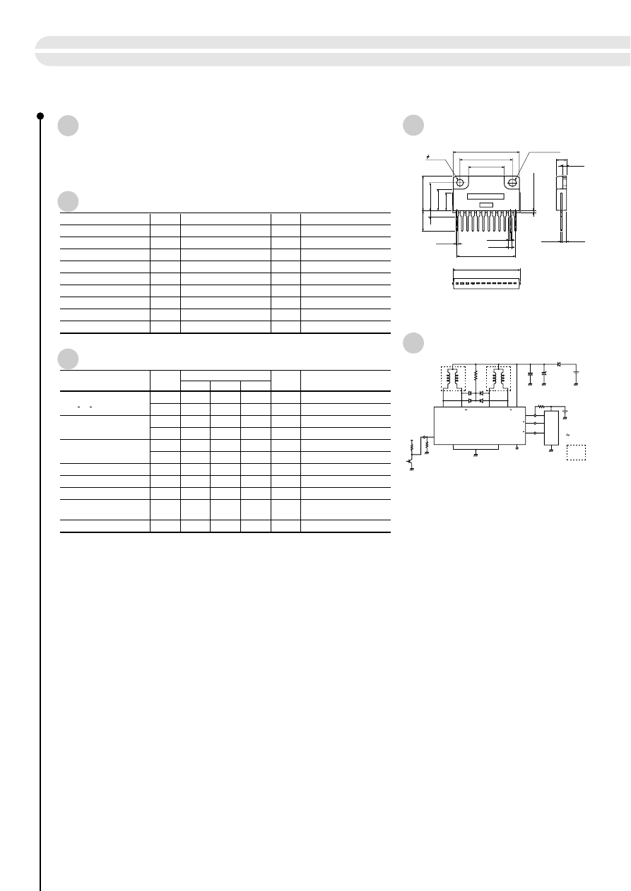
OUT
A
OUT
A
4
5
STBY
P-GND
L-GND
L-GND
9
8
1
C
12
3
10
2
6
11
7
N.C.
4.7 k
Ω
OUT
B
OUT
B
V
S
DIAG
I
A /A
I
B/B
ZD: V
S
<35V
C 100
µ
F
(Reference)
Stepper
motor
SLA4708M
CPU
ZD
5V
+
Standard Circuit Diagram
External Dimensions
(unit: mm)
Stepper-motor Driver ICs SLA4708M
46
Features
●
High output breakdown voltage of 50V
●
Affluent output current of 1.5A
●
Built-in overcurrent, overvoltage and thermal protection circuits
●
Low standby current of 50
µ
A
Parameter
Symbol
Unit
Conditions
Ratings
Absolute Maximum Ratings
Electrical Characteristics
Parameter
Symbol
min
typ
max
Unit
Conditions
Ratings
(Ta =25ºC)
Power supply voltage
Breakdown voltage
Input voltage
Input voltage
( I
A/A
, I
B/B
standby)
Input current
(V
S
=12V, Ta=25ºC)
Diagnostic output withstand voltage
Operating temperature
Storage temperature
Power Dissipation
V
S
V
O
V
IN
V
IL
V
IN
= 0.4V
2.4
50
0.8
50
V
–0.8
mA
V
V
IH
I
IL
V
IN
= 2.4V
I
O
= 1A, Ta
= 25ºC
µ
A
I
IH
Output saturation voltage
1.3
V
V
O.STA
I
O
= 1.5A, Ta
= 25ºC
V
O
= 16V
I
DIAG
= 5mA
V
S
= 12V
1.5
100
0.3
V
V
O.STA
Output leak current
µ
A
I
O. LEAK
1.8
Overcurrent detection
A
I
SD
27.5
Overvoltage detection
V
V
SD
Saturation voltage of diagnostic
output
V
V
DIAG.L
Standby current
µ
A
I
STB
I
DIAG
I
DIAG. H
Top
Tstg
P
D
V
V
Without heatsink
V
mA
V
ºC
ºC
W
35
50
–0.3 to +7
Output current
Diagnostic output sink current
I
O, AVE
A
1.5
10
7
–40 to +85
–40 to +150
3.5 (Ta=25ºC)
1 2 3
11•P2.54
±
0.7
=27.94
±
1.0
31.5 max
0.85
1.2
±
0.15
31.0
±
0.2
24.4
±
0.2
16.4
±
0.2
3.2
±
0.15
Ellipse 3.2
±
0.15
• 3.8
0.55
2.2
±
0.7
1.7
±
0.7
4.8
±
0.2
1.45
±
0.15
Pin 1
12
4 5 6 7 8 9 10 11 12
8.5
m
a
x
9
.5
min (10.4)
Lead plate thickness
resins
0.8
max
9.9
±
0.2
13.0
±
0.2
16.0
±
0.2
2.7
+0.2
–0.1
+0.2
–0.1
a: Part No.
b: Lot No.
a
b

0
0
10
20
30
Power supply voltage V
S
(V)
20
10
0
200
At standby I
S
(
µ
A)
Power supply current
At Constant I
S
(mA)
Constant (S
T
= 5V)
At standby (S
T
= 0V)
100
0
10
20
30
0
10
12
14
2
4
6
8
Output voltage V
O
(V)
Power supply voltage V
S
(V)
35
=
T 25ºC
a
V 12V
cc=
Common for
all phases
0
1.0
2.0
3.0
0
1.0
2.0
Saturation voltage of output transistor Vsat (V)
Output current I
O
(A)
Ta =25ºC
Common for
all phases
0.5
1.5
0
0
Output voltage V
O
(V)
Junction temperature Tj (ºC)
=
V 5V
ST
10
Vcc (Vs) =12V
110
120
130
140
150
160
j2
T
j1
T
14
12
2
4
6
8
47
■
Power Supply Current Characteristics
■
Overvoltage Protection Characteristics
■
Saturation Voltage of Output Transistor Characteristics
■
Thermal Protection Characteristics
Vcc (Vs) =16V
Electrical Characteristics
SLA4708M
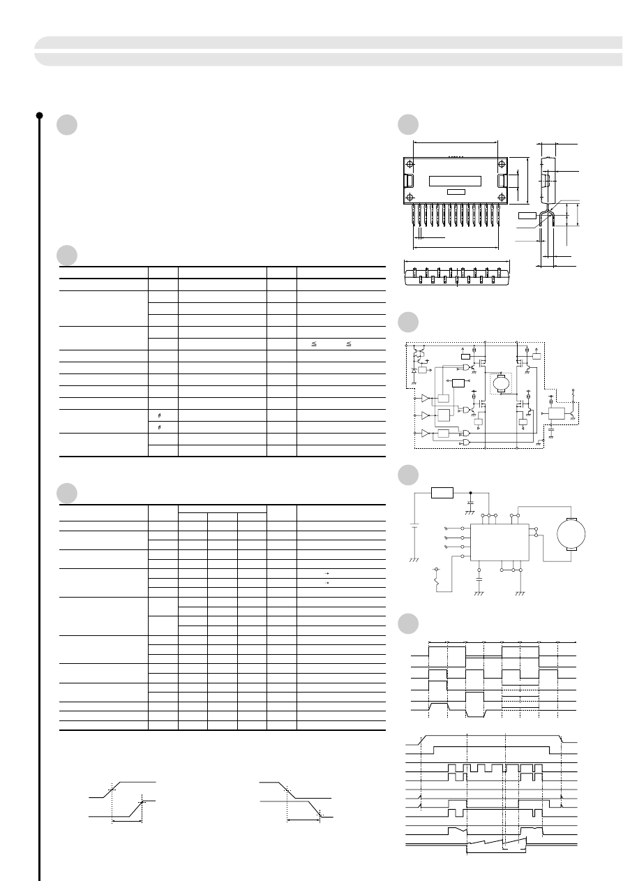
Parameter
Symbol
Unit
Conditions
Ratings
Absolute Maximum Ratings
Electrical Characteristics
Parameter
Symbol
min
typ
max
Unit
Conditions
Ratings
(Ta =25ºC)
Motor supply voltage
Input terminal voltage
PWM control frequency
Forward • reverse rotation switch frequency
Power dissipation
Input terminal voltage
Input terminal current
Motor supply voltage
Output saturation voltage
Static circuit current
DIAG output pulse width
DIAG terminal voltage
(Unless, otherwise specified, Tj=Tch=25
°
C, V
M
=14V, I
O
=3A)
Output leakage current
Junction and channel temperature
Operating temperature
Storage temperature
V
M
IN1
IN2
PWM
f
PWM
V
IN
I
O
=3A
V
M
=40V
V
M
=40V
V
IN
1=V
IN
2=V
PWM
Brake mode
V
IN
1=V
IN
2=V
PWM
V
IN
1=V
IN
2=V
PWM
=0V
V
IN
1=V
IN
2=V
PWM
=5V
I
O
=10A
I
O
=3A
I
O
=10A
I
O
=3A
V
PWM
: H L (Vth=2.5V typ)
Stop mode
Forward and reverse mode
C=1
µ
F (typ)
ID • SINK=1mA
V
0.3
6
18
V
100
µ
A
100
µ
A
V
2.0
V
200
µ
A
22
1.0
0.8
1.0
0.8
22
16
0.3
µ
A
V
mA
mA
mA
ms
V
V, V
O
-PG
I
O
=3A
V
M
=24V (2 min.)
0.8
V
Output transmission time
Forward voltage
characteristic of diode
between drain and source
V
PWM
: L H (Vth=2.5V typ)
3.0
–100
10
15
10
µ
s
µ
s
µ
s
V
V
V
tpLH
tpHL
tpHL-tpLH
V
F
• L
V
F
• H
I
L
, L
V, V
M
-V
O
I
L
, H
V
IN
, H
V
IN
, L
I
IN
, L
I
IN
, H
OPC start current
16
20
A
I
OCP
IM1
IM2
IM3
t
DIAG
V
D
• L
f
CW
P
D1
P
D2
Tj, Tch
T
OP
Tstg
V
V
V
V
Without heatsink
With infinite heatsink
Duty=20% to 80%
P
W
1ms, Duty 50%
kHz
Hz
W
W
ºC
ºC
ºC
40
–0.3 to 7
–0.3 to 7
–0.3 to 7
20
500
Output current
I
O
I
O (p-p)
A
A
±
5
±
17
3.6
33.7
–40 to +150
–40 to +85
–40 to +150
Thermal resistance
j-c
ºC/W
3.7
j-a
ºC/W
35
Standard Connection Diagram
Equivalent Circuit
Timing Chart
External Dimensions
(unit: mm)
Features
●
P-ch MOS for high side and N-ch MOS for low side in one package
●
Enable to drive DC
±
5V
●
Possible to drive a motor at the LS-TTL, C-MOS Logic level
●
Guarantee Tj=Tch=150
°
C
●
Built-in over current protection and thermal shut down circuits
●
Built-in diagnosis function to monitor and signal the state of each protection circuits
●
Built-in vertical current prevention circuits (Dead time is defined internally.)
●
No insulator required for Sanken's original package (SPM package)
48
Full Bridge PWM Control DC Motor Driver IC SI-5300
*
*
2
*
3
*
1
*
4
Note:
*
1
: The standard value of I
OCP
is assumed to be a value by which the output of each Power MOS FET cuts off. When the
protection circuit of OCP and TSD operates, Power MOS FETs keeps cutoff. When a signal (5V: H
➞
0V: L) is input to the
terminal PWM, the cutoff operation will be released. Moreover, three minutes (Ta=25ºC, f
PWM
=10kHz, V
M
=14V) are assumed
to be max at the overcurrent state continuance time in the V
M
operation and the ground of output terminal (OUT1, OUT2).
It is not the one to assure the operation including reliability in the state that the short-circuit continues for a long time.
Output transmission
time tpHL is time from
Vth (2.5V typ) of the
terminal of PWM to
output (V
OUT
*
0.1) of
the output terminal.
Output transmission
time tpLH is time from
Vth (2.5V typ) of the
terminal of PWM to
output (V
OUT
*
0.9) of
the output terminal.
a: Part No.
b: Lot No.
0.75
+0.2
–0.1
16.1
±
0.2
a
b
(28.4)
(4.5)
14
•
P2.03
±
0.1
=(28.42)
35
±
0.3
1 2 3 4 5 6 7 8 9 10 11 12 13 14 15
0.45
+0.2
–0.1
7.6
±
0.5
3.6
±
0.5
(4
)
4.8
±
0.2
2.7
±
0.2
2
±
0.5
4.5
±
0.7
(R0.8)
(R0.8)
R-end
Protection circuit
V
M
=2V
V
M
=2V
V
M
V
M-OUT1
(Pch1 V
DS
)
V
OUT1-GND
(Nch1 V
DS
)
V
OUT2-GND
(Nch2 V
DS
)
OUT1
OUT2
TDIAG
DIAG
20ms
(min)
DIAG Threminal
V
CC
=5V Pull-up
I
OUT
(A)
V
M-OUT2
(Pch2 V
DS
)
IN1
IN2
PWM
Return to constant action
Therminal name
IN1
IN2
PWM
OUT1
GND
OUT2
I
OUT
(A)
Forward
Duty ON
Forward
Duty OFF
Reverse
Duty ON
Reverse
Duty OFF
Stop
(Free Run)
Stop
(Free Run)
High inpidance
High inpidance
High inpidance
M
V
M
V
M
OUT1
OUT2
V
M
IN1
IN2
PGND
PGND
LGND
DIAG
T
DIAG
C
DIAG
1
µ
F
ECU inside
V
CC
PULL-UP
Resistor
PWM
Pre-Rec
TSD
B
B
B
B
B
Pch1
Pch2
Nch1
Nch2
B
A
A
A
A
A
A
FF
Q
S
R
Dead
Time
Dead
Time
PWM
down
edge
sense
OCP
OCP
DIAG
CONTROL
OCP
OCP
SI-5300
14, 15
OUT2
1, 2
OUT1
3, 5, 13
V
M
Relay
Battery
Capacitor
220
µ
F
CPU
6 IN1
11 IN2
7 PWM
10 DIAG
9
T
DIAG
V
CC
8
LGND
4,12
PGND
Delay Capacitor
1
µ
F
+
Pull-up Resistor
10k
Ω
(Open Collector)
M
GND
Vth
V
PWM
(5V)
V
OUT
V
OUT
*
0.9
GND
tpLH
PWM terminal
OUT terminal
Vth
V
PWM
(5V)
V
OUT
*
0.1
GND
GND
tpHL
PWM terminal
OUT terminal
*
4: DIAG signal output terminal is an open collector output. Use a pull-up resistor when connecting it to a logic circuit.
*
3: Output transmission time (tpHL)
*
2: Output transmission time (tpLH)
Breake
Breake
Note:
*
The dead time for the length current prevention in positive and the reversing switch is set by
internal control IC. The set point in internal IC at the dead time is 20
µ
s (typical).
Please take into account the dead time and consider the load conditions when you use the IC.
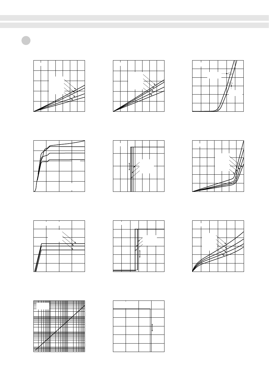
Duty on
■
Output saturation voltage (Pch)
■
Quiescent circuit current
■
Output saturation voltage (Nch)
■
Voltage of input terminal (Threshold voltage)
■
V
TDIAG
– V
DIAG
Characteristics
■
Forward voltage of Diode between drain and source
■
Current of input terminal (SINK current)
■
DIAG terminal • Saturation voltage
■
Current of input terminal (Source current)
■
DIAG terminal • Output pulse width
■
Thermal shut down protection
0
0
1
2
3
4
5
6
7
V•
V
M
-V
O
(V)
1.0
0.8
0.6
0.4
0.2
0
10
20
40
30
I
M
(mA)
V
M
(V)
0
0
–2
–4
–6
–8
–10
–12
10
20
40
30
I
IN1
, I
IN2
, PWM
source
(
µ
A)
V
M
(V)
0.01
µ
0.1
µ
1
µ
10
µ
1
10
100
1000
DIAG terminal • Output time of low signal (ms)
TDIAG terminal Delay capacitor capacitance
0
0
1
2
3
4
5
6
1
2
3
4
5
6
V
DIAG
(V)
V
TDIAG
(V)
100
125
150
175
200
1
2
3
4
5
6
0
V
DIAG
(V)
Ta (ºC)
0
0
0.1
0.2
0.3
0.4
0.5
0.6
1
2
3
4
5
6
V
DIAG
(V)
I
SINK
(mA)
I
O
(A)
0
0
1
2
3
4
5
6
7
0
1
2
3
4
5
6
7
4
8
12
16
V
IN1, IN2
, PWM (V)
0
0
1
2
3
4
0.1
0.2
0.3
0.4
0.5
0.6
5
6
7
I
SINK
(mA)
V
IN1, IN2
, PWM (V)
0
0
0.2
0.4
0.6
0.8
1.0
1.2
2
4
6
8
12
10
I
FSD
(A)
V
FSD
(V)
0
0.1
0.2
0.3
0.4
0.5
I
O
(A)
V•
V
O
-P
G
(V)
V
O
(V)
V
M
=14V
Ta=25
ºC
V
M
=14V
V
M
=14V
Ta=150ºC
Ta=85ºC
Ta=25ºC
Ta=–40ºC
Ta=150ºC
Ta=85ºC
Ta=25ºC
Ta=–40ºC
Ta=150ºC
Ta=85ºC
Ta=25ºC
Ta=–40ºC
Nch
MOS FET
Pch
MOS FET
V
M
=14V
Ta=150ºC
Ta=25ºC
Ta=–40ºC
Ta=150ºC
Ta=25ºC
Ta=–40ºC
Ta=150ºC
Ta=25ºC
Ta=–40ºC
I
IN
1=I
IN
2=PWM=0V
Ta=
25ºC
V
M
=14V
V
M
=10V
I
O
=0A
V
M
=14V
V
M
=14V
Ta=150ºC
Ta=85ºC
Ta=25ºC
Ta=–40ºC
Electrical Characteristics
49
Pull-up resistance =3k
Ω
0
5
10
15
20
25
I
O
=0A
Ta=
25ºC
Brake
Duty off
Stop
SI-5300

■
Pch MOS FET Safe Operating Area (SOA)
■
Nch MOS FET Safe Operating Area (SOA)
2
10
40
100
0.3
1
10
100
0.3
1
10
100
I
OUT
(A)
I
OUT
(A)
V
M-OUT
(V)
2
10
40
100
V
OUT -PG
(V)
■
P
D
—Ta Characteristics
–40 –30
0
25
50
75
100
0
5
10
15
20
25
30
35
40
Allowable Power Dissipation P
D
(W)
Ambient temperature Ta (ºC)
Tc=25ºC
Infinite heatsink (Tc =25ºC)
No heatsink
1ms
10ms
100ms
Tc=25ºC
1ms
10ms
100ms
50
Electrical Characteristics
Full Bridge PWM Control DC Motor Driver IC SI-5300

51
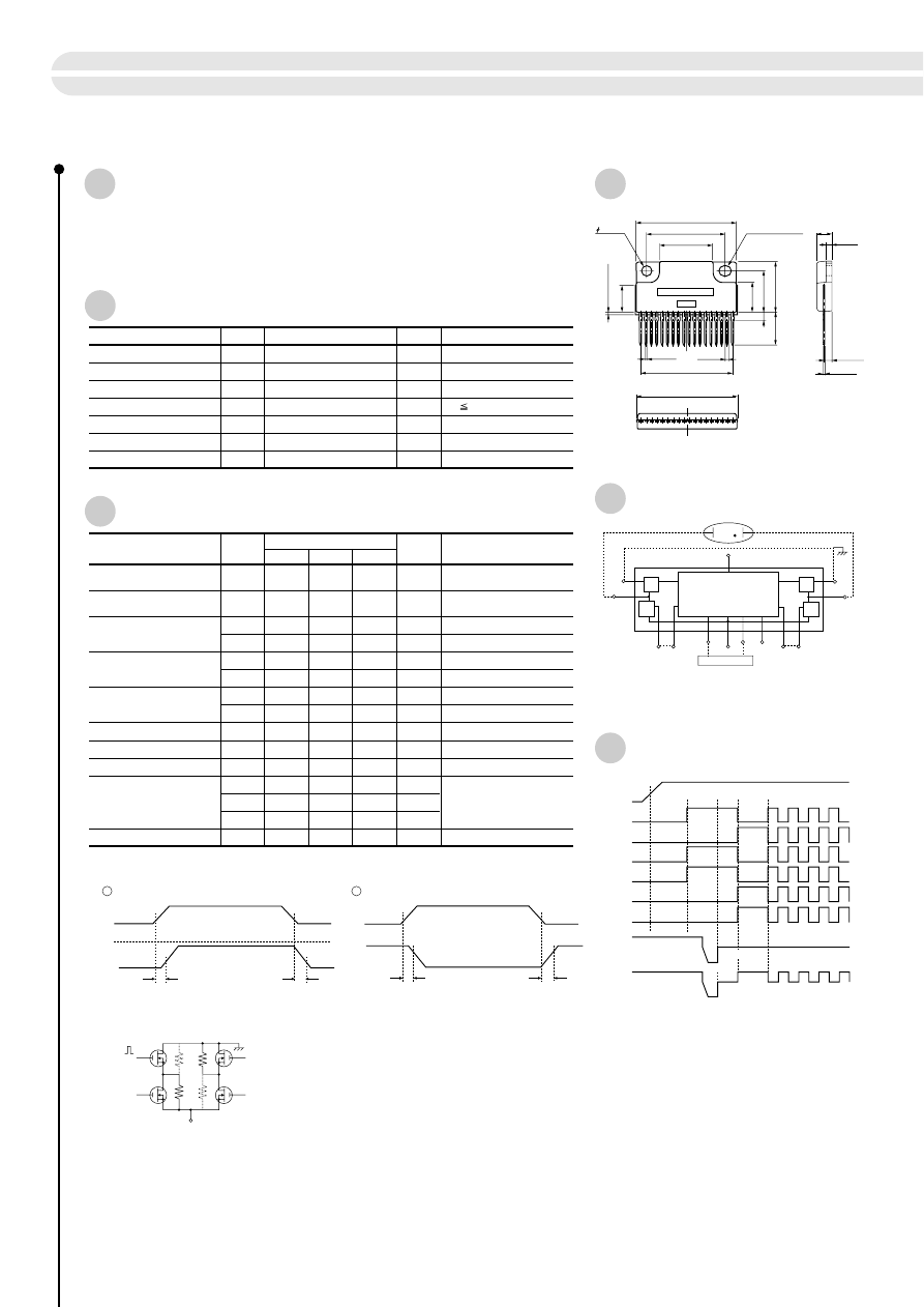
Electrical Characteristics
Parameter
Symbol
min
typ
max
Unit
Conditions
Ratings
Power MOS FET output
leakage voltage
High-side Power MOS FET
output on-state voltage
Power MOS FET output
breakdown voltage
Delay time
BV
OUT
I
O
=0.4A, V
IN
=10V
V
O
=500V
I
O
=100
µ
A
I
O
=2A, V
IN
=10V
V
CC
=10V, V
M
=400V
V
CC
=4.5 to 15V
V
CC
=10A, V
IN
=10V,
V
M
=85A,
I
O
=0.41A
V
CC
=4.5 to 15V
V
500
0.28
0.4
1.4
2.0
100
µ
A
0.52
2.6
V
V
4.0
mA
0.8V
CC
V
1.4
V
µ
s
0.2V
CC
V
I
OUT (off)
V
OUT (on)
1
V
OUT (on)
2
Low-side Power MOS FET
output on-state voltage
I
O
=0.4A, V
GL
=10V
I
O
=2A, V
GL
=10V
0.28
0.4
1.4
2.0
0.52
2.6
V
V
V
OUT (on)
1
V
OUT (on)
2
Quiescent circuit current
V
CC
=4.5 to 15V
V
CC
=10V, V
M
=400V
3.0
4.0
mA
mA
I
CC
1
I
CC
2
I
CC
3
V
IH
V
IL
t
d (on)
3.3
µ
s
t
d (off)
–40 to +105ºC
2.5
15
µ
s
∆
t
V
CC
Input voltage (Low level)
Operating voltage
Operating circuit current
Input voltage (High level)
Parameter
Symbol
Unit
Conditions
Ratings
Absolute Maximum Ratings
Power source voltage
Input voltage
Output voltage
Output current
Power dissipation
Storage temperature
Operation temperature
V
M
V
IN
V
O
I
O
P
D
Tstg
Topr
V
V
V
A
W
ºC
ºC
500
15
500
15
5 (Ta=25ºC)
–40 to +125
–40 to +105
*
Block Diagram
Timing Chart
External Dimensions
(unit: mm)
52
Features
●
One Package Full Bridge Driver Consisted of High Voltage IC and Power
MOS FETs (4 pieces)
●
High Voltage Driver which accepts direct connection to the input signal line
●
External components such as high voltage diodes and capacitors are not required
High Voltage Full Bridge Drive IC SLA2402M
*
Power GND (D terminal) to -HV (-HV terminal) voltage.
*
31.0
±
0.2
4.8
±
0.2
1.7
±
0.1
24.4
±
0.2
16.4
±
0.2
16.0
±
0.2
2.45
±
0.2
9.9
±
0.2
13.0
±
0.2
2.7
Ellipse
3.2
±
0.15
•3.8
3.2
±
0.15
17• P1.68
±
0.1
=28.56
8.5 max
31.5 max
9.5 min
Lead plate thickness
resins
0.8
max
0.65
+0.2
–0.1
+0.2
–0.1
+0.2
–0.1
1.0
0.55
4
2
3
6
8
10
9
11
13
16
17
15
7
+12V
OUT1
OUT2
GL1
GL2
HO2
LO2
HO1
MIC
CPU
V
CC
V
IN
1
V
IN
2
–HV
LO1
D1
MOSQ1
MOSQ2
MOSQ'1
MOSQ'2
L GND
*
Dotted Line: Outside Connection
V
CC
IN1
IN2
HO1
HO2
LO2
LO1
OUT2-GND
—HV
0V
–400V
–100V
OSC 400Hz
Ignition
V
IN
1
0V
0V
10%
10%
10%
10%
V
OUT
1
td (on)
td (on)
10%
10%
10%
10%
V
IN
1
0V
0V
V
OUT
2
td (on)
td (on)
Highside switch turn-on, turn-off
Lowside switch turn-on, turn-off
*
About delay time
Signal input waveform vs output waveform
*
∆
t:
∆
t = td (on) – td (off)
Measurement Circuit
V
IN
1
V
IN
2
V
M
V
OUT
1
V
OUT
2
V
IN
2
V
IN
1
R
L
Conditions
V
CC
=10V, V
IN
=10V (pulse)
V
M
=85V
I
O
=0.41A (R
L
=207
Ω
)
*
Without heatsink
P
W
250
µ
s
a: Part No.
b: Lot No.
1
2
a
b
When pulse signal is inputted to V
lN1
,
R
L
on solid line is ON and dotted line
R
L
is off.
On the contrary, when pulse signal is
inputted to V
lN2
, R
L
on dotted line is
ON and dotted line R
L
is off.
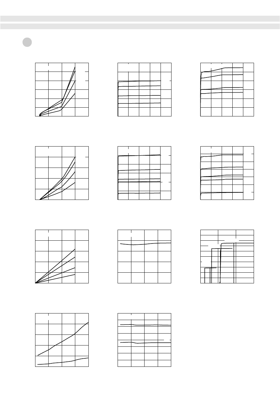
■
Quiescent circuit current
■
Quiescent circuit current supplied high voltage
■
Quiescent circuit current supplied high voltage
■
Quiescent circuit current
■
Operating circuit current
■
Operating circuit current
0
0
5
10
15
20
0.5
1.0
1.5
2.0
2.5
3.0
Quiescent circuit current I
CC
1
(mA)
Operation voltage V
CC
(V)
–40ºC
V
IN
=0V
0
0
5
10
15
20
1
2
3
4
5
Quiescent circuit current I
CC
2 (mA)
Operation voltage V
CC
(V)
150ºC
105ºC
25ºC
150ºC
105ºC
25ºC
–40ºC
0
0
1
2
3
4
2
4
6
8
10
0
2
4
6
8
10
1
0
2
3
4
5
6
7
8
Output on-state voltage
(V)
Output current (A)
Ambient temperature (ºC)
Input voltage V
IN
(V)
–50
0
0
50
100
150
–50
0
50
100
150
–50
0
50
100
150
0
2
4
6
8
10
0
5
10
15
1
2
3
4
5
Output on-state voltage
(V)
Gate drive voltage V
GL
(V)
Gate drive voltage V
GL
(V)
Input threshold voltage V
IH
, V
IL
(V)
Ambient temperature (ºC)
Ambient temperature (ºC)
V
IN
=0V
V
M
=400V
0
0
100
200
300
500
400
0.5
1.0
1.5
2.0
2.5
3.0
Quiescent circuit current I
CC
2
(mA)
High voltage V
M
(V)
150ºC
105ºC
25ºC
–40ºC
V
IN
=0V
V
CC
=10V
0
0
100
200
300
500
400
0.5
1.0
1.5
2.0
2.5
3.0
Quiescent circuit current I
CC
2
(mA)
High voltage V
M
(V)
V
CC
=
15V
12V
10V
4.5V
9V
Ta=25ºC
Ta=25ºC
0
0
100
200
300
500
400
0.5
1.0
1.5
2.0
2.5
3.5
■
Gate drive voltage
■
Input threshold voltage
■
Output on-state voltage
■
Output on-state voltage
■
Gate drive voltage
3.0
Operating circuit current I
CC
3
(mA)
High voltage V
M
(V)
V
CC
=
15V
12V
10V
4.5V
9V
Ta=25ºC
0
0
100
200
300
400
500
0.5
1.0
1.5
2.0
2.5
3.0
Operating circuit current I
CC
3
(mA)
High voltage V
M
(V)
150ºC
105ºC
25ºC
–40ºC
V
CC
=V
IN
1(2)=10V
V
CC
=10V
V
CC
=15V
V
CC
=
4.5V
V
CC
=9V
V
CC
=10V
I
O
=2A
I
O
=0.4A
V
IH
V
IL
V
CC
=V
IN
=10V
V
CC
=V
IN
=10V
150ºC
105ºC
25ºC
–40ºC
Electrical Characteristics
53
SLA2402M

■
High side switch turn-on, off
■
High side switch turn-on, off
■
Low side switch turn-on, off
■
Low side switch turn-on, off
■
Power derating curve
■
Transient thermal resistance characteristics
■
Safe operating area (Power MOS FET)
4
6
8
10
12
14
16
0
1.0
2.0
3.0
4.0
5.0
turn-on, off
(
µ
s)
Operation voltage V
CC
(V)
turn-on
turn-off
4
6
8
10
12
14
16
0
1.0
2.0
3.0
4.0
5.0
turn-on, off
(
µ
s)
Operation voltage V
CC
(V)
turn-on
turn-off
Ta=25ºC
V
M
=85V, I
O
=0.41A
–50
0
50
100
150
0
1.0
2.0
3.0
4.0
5.0
turn-on, off
(
µ
s)
Ambient temperature (ºC)
turn-on
turn-off
V
M
=85V, I
O
=0.41A
V
CC
=10V
–50
0
50
100
150
0
1.0
2.0
3.0
4.0
5.0
turn-on, off
(
µ
s)
Ambient temperature (ºC)
turn-on
–50
0
50
100
150
0
2
1
3
4
5
6
Power dissipation
(W)
Ambient temperature (ºC)
turn-off
V
M
=85V, I
O
=0.41A
V
CC
=10V
Ta=25ºC
V
M
=85V, I
O
=0.41A
0.0001 0.001
0.01
0.1
1
10
100
0.001
0.01
0.1
1
10
100
Transient thermal resistance
(º
C/
W
)
Power time (s)
Ta=25ºC
Single pulse
10
1000
100
0.01
0.1
1
10
100
Drain current
(A)
Drain to source voltage (V)
Ta=25ºC
Single pulse
RDS (on)
limited
1ms
10ms
100
µ
s
without heatsink
54
Electrical Characteristics
High Voltage Full Bridge Drive IC SLA2402M

55
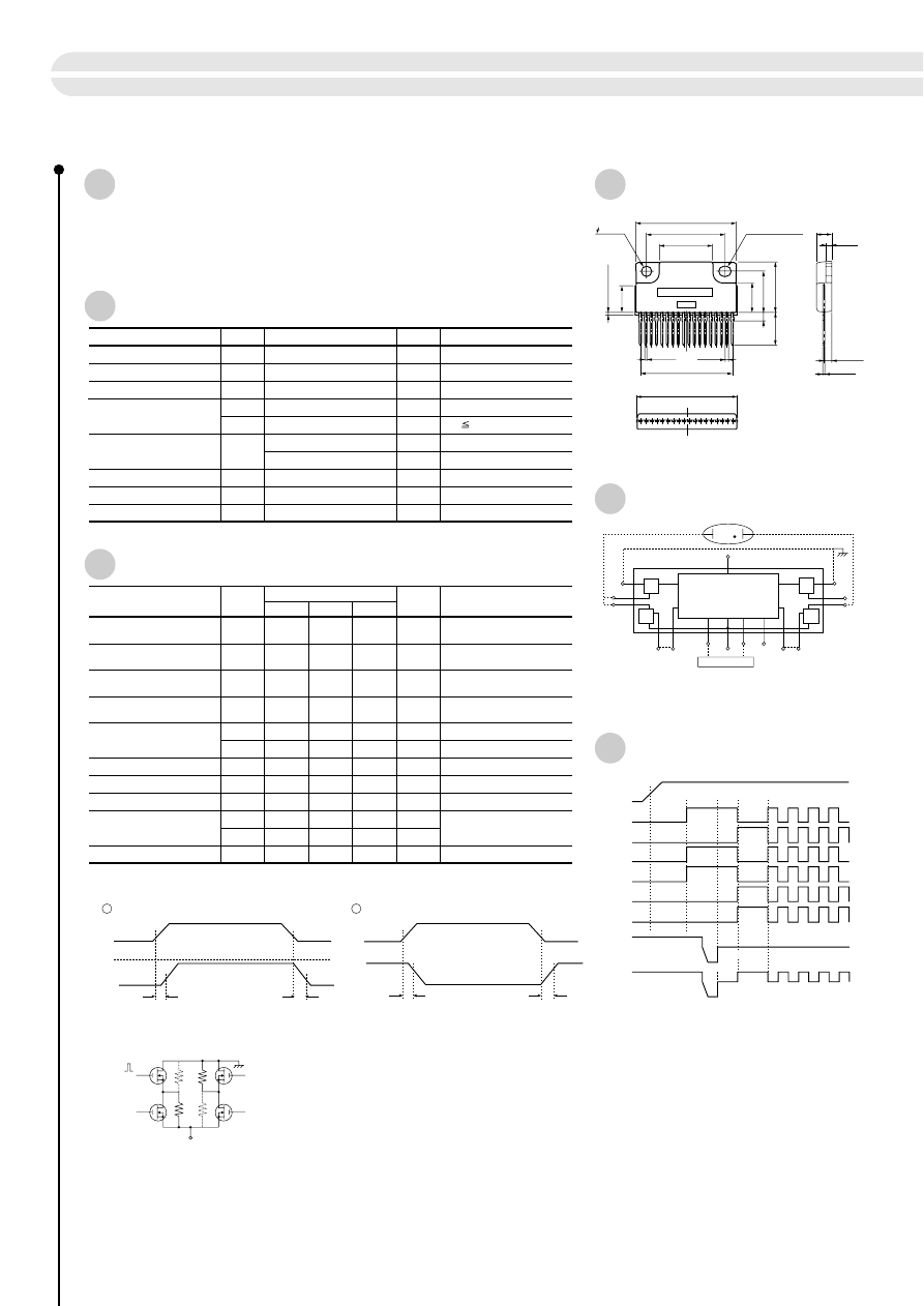
Electrical Characteristics
Parameter
Symbol
min
typ
max
Unit
Conditions
Ratings
Power MOS FET output
leakage voltage
High-side Power MOS FET
output on-state voltage
Power MOS FET output
breakdown voltage
Delay time
BV
OUT
I
O
=0.4A, V
IN
=10V
V
O
=500V
I
O
=100
µ
A
V
CC
=10V, V
M
=400V
V
CC
=6 to 15V
V
CC
=10A, V
IN
=10V,
V
M
=85V, I
O
=0.41A
V
CC
=6 to 15V
V
500
0.18
0.26
100
µ
A
0.34
V
4.0
mA
0.8V
CC
V
2.0
V
µ
s
0.2V
CC
6
V
I
OUT (off)
V
OUT (on)
Lowside Power MOS FET
output on-state voltage
I
O
=0.4A, V
GL
=10V
0.18
0.26
0.34
V
V
OUT (on)
Quiescent circuit current
V
CC
=6 to 15V
V
CC
=10V, V
M
=400V
3.0
4.0
mA
mA
I
CC
1
I
CC
2
I
CC
3
V
IH
V
IL
t
d (on)
3.0
µ
s
t
d (off)
–40 to +125ºC
15
V
CC
Input voltage (Low level)
Operating voltage
Operating circuit current
Input voltage (High level)
Parameter
Symbol
Unit
Conditions
Ratings
Absolute Maximum Ratings
Power source voltage
Input voltage
Output voltage
Output current
Power dissipation
Storage temperature
Operation temperature
V
M
V
IN
V
O
I
O
P
D
Tstg
Topr
V
V
V
A
W
A
W
Tc=25ºC
Without heatsink
With infinite heatsink
ºC
ºC
500
15
500
7
I
O (peak)
15
5 (Ta=25ºC)
40 (Tc=25ºC)
–40 to +125
–40 to +125
Junction temperature
Tj
ºC
150
*
56
Features
●
One Package Full Bridge Driver Consisted of High Voltage IC and Power
MOS FETs (4 pieces)
●
High Voltage Driver which accepts direct connection to the input signal line
●
External components such as high voltage diodes and capacitors are not required
High Voltage Full Bridge Drive IC SLA2403M
*
Power GND (D terminal) to -HV (-HV terminal) voltage.
*
Block Diagram
*
Dotted Line: Outside Connection
4
3
5
2
6
8
10
9
11
13
17
14
16
15
D2
7
OUT1
OUT2
GL1
GL2
HO2
LO2
HO1
MIC
CPU
V
CC
V
IN
1
V
IN
2
–HV
LO1
D1
MOSQ1
MOSQ2
MOSQ'1
MOSQ'2
L GND
V
IN
1
0V
0V
10%
10%
10%
10%
V
OUT
1
td (on)
td (on)
10%
10%
10%
10%
V
IN
1
0V
0V
V
OUT
2
td (on)
td (on)
Highside switch turn-on, turn-off
Lowside switch turn-on, turn-off
*
About delay time
Signal input waveform vs output waveform
*
∆
t:
∆
t = td (on) – td (off)
Measurement Circuit
V
IN
1
V
IN
2
V
M
V
OUT
1
V
OUT
2
V
IN
2
V
IN
1
R
L
Conditions
V
CC
=10V, V
IN
=10V (pulse)
V
M
=85V
I
O
=0.41A (R
L
=207
Ω
)
1
2
External Dimensions
(unit: mm)
31.0
±
0.2
4.8
±
0.2
1.7
±
0.1
24.4
±
0.2
16.4
±
0.2
16.0
±
0.2
2.45
±
0.2
9.9
±
0.2
13.0
±
0.2
2.7
Ellipse
3.2
±
0.15
•3.8
3.2
±
0.15
17• P1.68
±
0.1
=28.56
8.5 max
31.5 max
9.5 min
Lead plate thickness
resins
0.8
max
0.65
+0.2
–0.1
+0.2
–0.1
+0.2
–0.1
1.0
0.55
Timing Chart
V
CC
IN1
IN2
HO1
HO2
LO2
LO1
OUT2-GND
—HV
0V
–400V
–100V
OSC 400Hz
Ignition
a: Part No.
b: Lot No.
a
b
P
W
250
µ
s
*
When pulse signal is inputted to V
lN1
,
R
L
on solid line is ON and dotted line
R
L
is off.
On the contrary, when pulse signal is
inputted to V
lN2
, R
L
on dotted line is
ON and dotted line R
L
is off.

■
Quiescent circuit current
■
Quiescent circuit current supplied high voltage
■
Quiescent circuit current supplied high voltage
■
Quiescent circuit current supplied high voltage
■
Operating circuit current
■
Operating circuit current
0
0
5
10
15
20
0.5
1.0
1.5
2.0
2.5
3.0
Quiescent circuit current I
CC
1
(mA)
Operation voltage V
CC
(V)
0
0
5
10
15
20
1
2
3
4
5
Quiescent circuit current I
CC
2
(mA)
Operation voltage V
CC
(V)
0
0
1
2
3
4
1
2
3
4
6
5
0
2
4
6
8
10
1
0
2
3
4
5
6
7
Output on-state voltage V
OUT (ON)
(V)
Output current I
OUT
(A)
Ambient temperature (ºC)
Input voltage V
IN
(V)
–50
0
0
50
100
150
–50
0
50
100
150
–50
0
50
100
200
150
0
2
4
6
8
10
0
5
10
15
1
2
3
4
Output on-state voltage V
OUT (ON)
(V)
Input threshold voltage V
IH
(V)
Gate drive voltage V
GL
(V)
Input threshold voltage V
IL
(V)
Ambient temperature (ºC)
Ambient temperature (ºC)
0
0
100
200
300
500
400
0.5
1.0
1.5
2.0
2.5
3.0
Quiescent circuit current I
CC
2
(mA)
High voltage V
M
(V)
0
0
100
200
300
500
400
0.5
1.0
1.5
2.0
2.5
3.5
3.0
Quiescent circuit current I
CC
2
(mA)
High voltage V
M
(V)
0
0
100
200
300
500
400
0.5
1.0
1.5
2.0
2.5
4.0
3.5
■
Input threshold voltage
■
Input threshold voltage
0
2
4
6
10
8
–50
0
50
100
150
Gate drive voltage V
GL
(V)
Ambient temperature (ºC)
■
Gate drive voltage
■
Output on-state voltage
■
Output on-state voltage
■
Gate drive voltage
3.0
0
0.5
1.0
1.5
2.0
2.5
4.0
3.5
3.0
Operating circuit current I
CC
3
(mA)
High voltage V
M
(V)
0
100
200
300
400
500
Operating circuit current I
CC
3
(mA)
High voltage V
M
(V)
V
IN
=0V
150ºC
125ºC
25ºC
85ºC
–40ºC
V
IN
=0V
V
M
=400V
150ºC
85ºC
125ºC
25ºC
–40ºC
V
IN
=0V
V
CC
=10V
Ta=25ºC
Ta=25ºC
Ta=25ºC
150ºC
125ºC
25ºC
85ºC
–40ºC
V
CC
=V
IN
1(2)=10V
V
CC
=15V
V
CC
=
6V
V
CC
=10V
V
CC
=V
IN
=10V
V
CC
=V
IN
=10V
–40ºC
150ºC
125ºC
25ºC
85ºC
V
CC
=
15V
12V
10V
6V
9V
V
CC
=
15V
10V
12V
6V
9V
I
O
=2A
I
O
=0.4A
150ºC
125ºC
85ºC
25ºC
–40ºC
V
CC
=10V
V
CC
=6V
V
CC
=10V
V
CC
=6V
V
CC
=10V
V
CC
=6V
Electrical Characteristics
57
SLA2403M
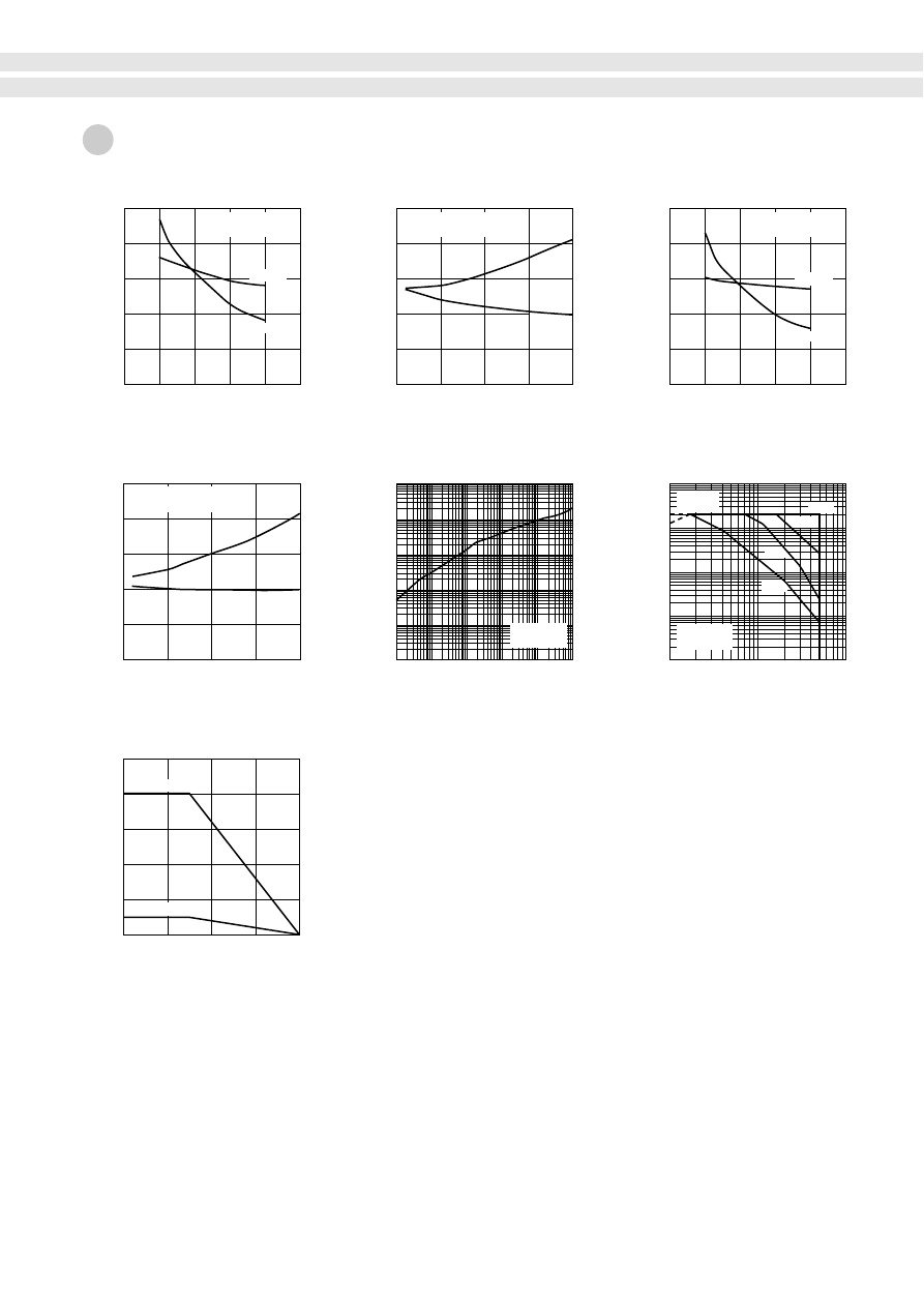
■
High side switch turn-on, off
■
High side switch turn-on, off
■
Low side switch turn-on, off
■
Low side switch turn-on, off
■
Power derating curve
■
Transient thermal resistance characteristics
■
Safe operating area (Power MOS FET)
4
6
8
10
12
14
0
1.0
2.0
3.0
4.0
5.0
turn-on, off
(
µ
s)
Operation voltage V
CC
(V)
4
6
8
10
12
14
0
1.0
2.0
3.0
4.0
5.0
turn-on, off
(
µ
s)
Operation voltage V
CC
(V)
–50
0
50
100
150
0
1.0
2.0
3.0
4.0
5.0
turn-on, off
(
µ
s)
Ambient temperature (ºC)
–50
0
50
100
150
0
1.0
2.0
3.0
4.0
5.0
turn-on, off
(
µ
s)
Ambient temperature (ºC)
–50
0
50
100
150
0
10
20
30
40
50
Power derating P
D
(W)
Ambient temperature (ºC)
0.001
0.01
0.1
1
10
100
0.001
0.01
0.1
1
10
100
Transient thermal resistance
(º
C/
W
)
Power time (s)
10
1000
100
0.01
0.1
1
10
100
Drain current
(A)
Drain to source voltage (V)
Ta=25ºC
Single pulse
Tc=25ºC
Ta=25ºC
Single pulse
without heatsink
turn-on
turn-off
V
M
=85V, I
O
=0.41A
V
CC
=10V
turn-on
turn-off
V
M
=85V, I
O
=0.41A
V
CC
=10V
turn-on
turn-off
Ta=25ºC
V
M
=85V, I
O
=0.41A
turn-on
turn-off
Ta=25ºC
V
M
=85V, I
O
=0.41A
1ms
10ms
100
µ
s
10
µ
s
RDS (on)
limited
58
Electrical Characteristics
High Voltage Full Bridge Drive IC SLA2403M

59
Unipolar Switch
Bipolar Switch
Bipolar Latch
Gear Tooth Sensor
Ratiometric, Linear Sensors
Subassembly
60
Magnetic Characteristics [mT] (Ta=25ºC)
Temperature Range
(ºC)
Package
Part No.
Remarks
A3121L
✽
A3122L
✽
A3123L
✽
A3141L
✽
A3142L
✽
A3143L
✽
A3144L
✽
A3240L
✽
A3250L
✽
B
HYS
(min)
B
RP
(min)
B
OP
(max)
45
7
UA / LT
High-Sensitive
High-Sensitive
High-Sensitive
High-Sensitive
Ultra-High-Sensitive, Chopper-Stabilized
Programmable, Chopper-Stabilized
Suffix ‘
✽
’ is package option
Suffix ‘
✽
’ is package option
Suffix ‘
✽
’ is package option
1, 2
12.5
40
7
UA / LT
1, 2
14
44
7
UA / LT
1, 2
18
16
2
UA / LT
1, 2
1
23
3
UA / LT
1, 2
7.5
34
3
UA / LT
1, 2
16.5
35
2
UA / LT
1, 2
5
5
1 (typ)
UA / LT / LH
1, 2, 3
0.5
Programmable
0.5
UA / LT
1, 2
B
OP
—B
HYS
–40 to +150
Magnetic Characteristics [mT] (Ta=25ºC)
Package
Part No.
Remarks
A3185L
✽
A3187L
✽
A3188L
✽
A3189L
✽
A3280L
✽
A3281L
✽
A3283L
✽
B
HYS
(min)
B
RP
(min)
B
OP
(max)
27
34
UA / LT
Chopper-Stabilized
Chopper-Stabilized
Chopper-Stabilized
1, 2
–27
15
10
UA / LT
1, 2
–15
18
20
UA / LT
1, 2
–18
23
10
UA / LT
1, 2
–23
4
4.5 (typ)
UA / LT / LH
1, 2, 3
–4
9
10 (typ)
UA / LT / LH
1, 2, 3
–9
18
30 (typ)
UA / LT / LH
1, 2, 3
–18
–40 to +150
Magnetic Characteristics [mT] (Ta=25ºC)
Package
Part No.
Remarks
A3134L
✽
UGS3132
✽
UGS3133
✽
B
HYS
(min)
B
RP
(min)
B
OP
(max)
5
1
UA / LT
High-Sensitive
1, 2
–5
9.5
3
UA / LT
1, 2
–9.5
7.5
3
UA / LT
1, 2
–7.5
–40 to +125
–40 to +150
Magnetic Characteristics [mT]
Temperature Range
(ºC)
Part No.
UGS3059KA
UGS3060KA
B
HYS
(min)
B
RP
(min)
B
OP
(max)
10
2
4
–10
3.5
1
4
–3.5
–40 to +150
Magnetic Characteristics [mT]
Temperature Range
(ºC)
Remarks
Part No.
A3515LUA
A3516LUA
Sense
50mV / mT
Chopper-Stabilized
1
25mV / mT
Chopper-Stabilized
1
–40 to +150
Application
Part No.
6
5
6
ATS610LSA
ATS611LSB
ATS612LSB
Large-tooth, gear-position sensing-crank angle, cam angle
Fine-pitch, large air gap, gear speed sensing-transmission speed ABS
Large / small-tooth gear-position sensing-crank angle, transmission speed, cam angle
Hall-Effect ICs
External
Dimensions
External
Dimensions
External
Dimensions
External
Dimensions
External
Dimensions
External
Dimensions
Temperature Range
(ºC)
Temperature Range
(ºC)
Figure 1 (UA)
Figure 4 (KA)
Figure 2 (LT)
Figure 3 (LH)
4.17
4.04
1.57
1.47
3.10
2.97
2.01
15.24
MIN
0.43
3
2
1
0.41
1.27
BSC
0.79
0.38
45
°
45
°
4.40
4.60
1.62
1.83
3.94
4.25
0.44
0.56
0.36
0.48
2.29
2.60
1.40
1.60
2.13
2.29
0.35
0.44
1.50
BSC
3.00
BSC
0.89
1.20
1
3
2
6.45
6.32
4.65
4.50
1.96
1
2
3
4
5
0.43
0.46
0.38
0.41
12.70
MIN
1.27
BSC
1.60
1.50
45
°
3.0
0.38
1
2
1.27
TYP
3
0.41
0.9 DIA
8.1
5.0 MIN
9.0
3.90
9.0
2.0
3.0
0.38
1
2
1.27
TYP
3
0.41
0.9 DIA
8.0
7.0 MIN
7.0
3.90
8.9
2.0
Figure 5 (SA)
Figure 6 (SB)
61
External Dimensions
(unit: mm)
3.10
2.90
0.45
0.30
3.00
2.70
0.95
BSC
2.10
1.85
0.55
REF
0.20
0.15
0.25 MIN
0º to 8º
2
1
3
1.10
0.90
1.25
0.90
0.15
0.00
Hall-Effect ICs
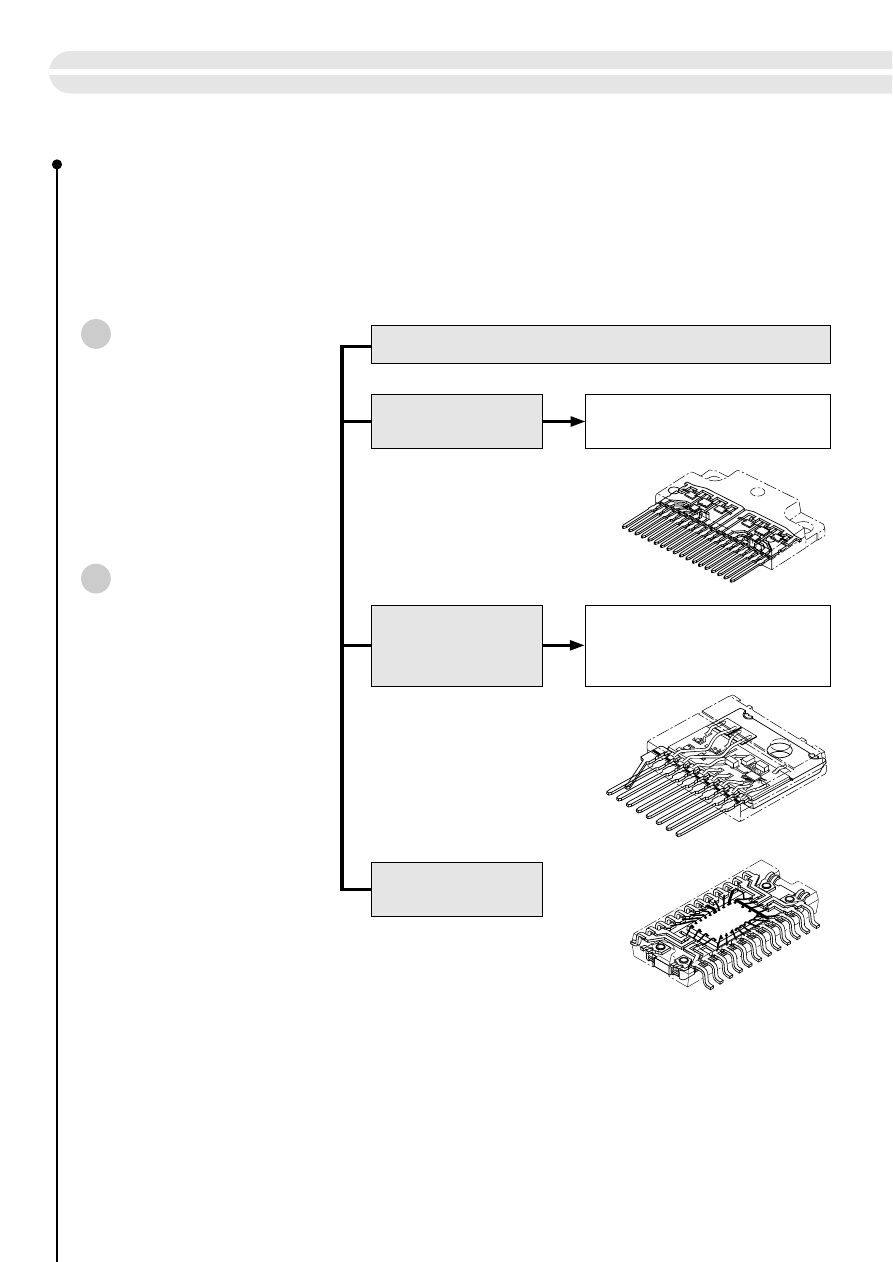
Custom IC
62
■
Various processing technologies of BIP, BiCMOS, CMOS and BCD can be used for the semiconductor chips.
■
Meets detailed user needs, especially power ICs. A wide range of general-purpose ICs is also available.
■
Employs a monolithic chip with flip-chip construction for increased reliability making it ideal for car electronic
devices.
■
Also available in hybrid ICs with transfer mold construction, multi-chip IC configuration and power monolithic
IC configuration.
Features
●
All semiconductor chips used are
manufactured by Sanken.
●
Main product lineup consists of
power ICs produced out of many
years' experience of Sanken.
●
Uses monolithic chips with flip-chip
construction.
●
Mainly available in miniature
transfer-mold packages.
Examples of Custom Hybrid IC
Products
●
Regulators for alternators
●
Igniters
●
Power supply for microcomputer
system
●
Power steering control IC
●
Motor and actuator driver
●
Others
Lead frame type
multi-chip power IC
●
One-chip power IC
Surface-mount
power IC
Lead frame type
power hybrid IC with
ceramic substrate
●
High-output high-breakdown voltage IC
●
Simplified integration of custom circuits
●
Distribution of unit functions
(Actuators may be built in the device)
Examples of Sanken Automotive Hybrid ICs
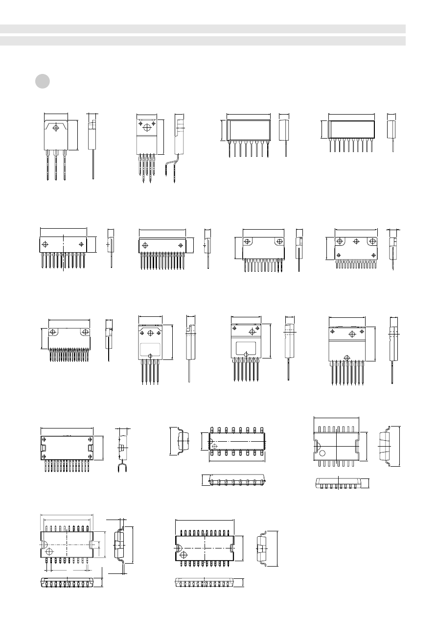
External Dimensions
(unit: mm)
63
STA 10pin
25.25
9.0
4.0
31.0
10.2
4.0
4.0
31.0
10.2
SMA15pin
SMA12pin
3GR-F
3GR-M
STR-S
SLA12pin
SPM
SMD16pin
SPF16pin
SPF24pin
SPF20pin
SLA15pin
SLA18pin
15.6
23
5.5
19.8
5.5
23
24.2
5.5
23
31.0
4.8
16
31.0
4.8
16.0
35
16.1
4.8
20.0
9.8
6.8
16
Pin 1
8
9
4.0
12.05
7.5
10.5
2.5
16 15 14 13 12 11 10
9
1
2
3
4
5
6
7
8
17.28
2.5
7.5
10.6
24
1
12
13
31.0
4.8
16.0
MT-100
FM205
5.0
10.0
16.9
4.2
15.6
19.9
20.2
4.0
9.0
STA 8pin
1.0
10.5
±
0.3
+0.1
–
0.05
0.25
+0.15
–
0.05
2.5
±
0.2
14.74
±
0.2
7.5
±
0.2
2
±
0.2
13.04
±
0.2
1.27
±
0.25
20
1
10
11
0.4
+0.15
–
0.05
Fin
thickness
Custom IC

Igniters
Injectors
AT (Automatic Transmissions)
Cruise controls
Airbag systems
Power steering
ABS
Electronic meters
Solenoid drivers
Clutch controls
Lamp controls
Others
74
80
73
75
79
84
85
86
99
90
105
91
66
66
68
72
87
67
88
89
66
78
93
94
95
96
97
98
102
104
70
81
82
83
100
103
104
71
92
101
69
77
76
2SD2141
MN638S
2SC4153
2SD2382
MN611S
STA461C
STA463C
STA464C
STA508A
SDC09
SDK09
SPF0001
2SA1488
2SA1488A
2SA1568
2SC4065
SLA8004
2SA1567
SDA03
SDA04
2SA1488
FP812
FKV460
FKV460S
FKV560
FKV560S
FKV660
FKV660S
SLA5027
SDK08
2SC3852
STA315A
STA335A
STA415A
STA509A
SDK06
SDK08
2SC4024
2SK2701
SMA5113
2SC3851
FN812
2SD2633
Application
Part No.
Page
Index by Application
64
Transistors and MOS FETs
Boosters for power supply
of microcomputers

Index by Load
Load
Current
Chip
Single
Single
Single
Single • 3
Single • 2
Single • 4
MOS • 4
MOS • 4
Single
Single
Single
Single • 4
Single • 2
MOS • 4
Single • 2
Single • 2
MOS • 4
MOS • 4
Single
Single
MOS
Single
Single
Single • 4
Single
Single
Single
Darlington
MOS • 4
MOS
MOS
MOS
MOS
MOS
MOS
Avalanche
Diode
TO220F
SPF
SD
STA
SMA
SLA
TO220S
Part No.
Single Package
Multi-chip Package
Remarks
2SA1488A
2SC3851
2SC3852
STA315A
STA335A
STA415A
STA509A
SDK06
2SA1488
2SC3851
2SC4153
SDA03
SDC09
SDK08
STA461C
STA463C
STA508A
SMA5113
2SA1567
2SD2382
2SK2701
FP812
FN812
SLA8004
2SA1568
2SC4024
2SC4065
2SD2141
SLA5027
FKV460
FKV560
FKV660
FKV460S
FKV560S
FKV660S
35V
35V
25W
25W
25W
13.5W
Es/b=50mJ
Es/b=150mJ
Es/b=50mJ
Es/b=40mJ
Es/b=40mJ
Es/b=45mJ
Es/b=45mJ
V
CEO
=120V
Es/b=80mJ
Es/b=80mJ
Es/b=80mJ
Es/b=45mJ
V
DSS
=450V
Es/b=200mJ
V
DSS
=450V
R
DS (ON)
=9m
Ω
max
R
DS (ON)
=11m
Ω
max
R
DS (ON)
=14m
Ω
max
R
DS (ON)
=9m
Ω
max
R
DS (ON)
=11m
Ω
max
R
DS (ON)
=14m
Ω
max
Es/b=210mJ
12W
18W
20W
18W
18W
4W
20W
35W
40W
40W
3W
3W
Single • 2
SDA04
2.8W
2.5W
3W
MOS
SDK09
3W
25W
25W
30W
60W
2.5W
Single
MN611S
Single • 2
SPF0001
35W
30W
35W
35W
35W
35W
35W
35W
35W
40W
40W
40W
60W
60W
60W
60W
35V
52V
52V
65V
115V
65V
115V
Single • 4
STA464C
65V
380V
Darlington
2SD2633
35W
Darlington
MN638S
380V
65
(Surface-mount) (Surface-mount)
Approx.
0.5A
Approx.
1.2A
Approx.
3A
Approx.
5A
10A
and over
Transistors and MOS FETs
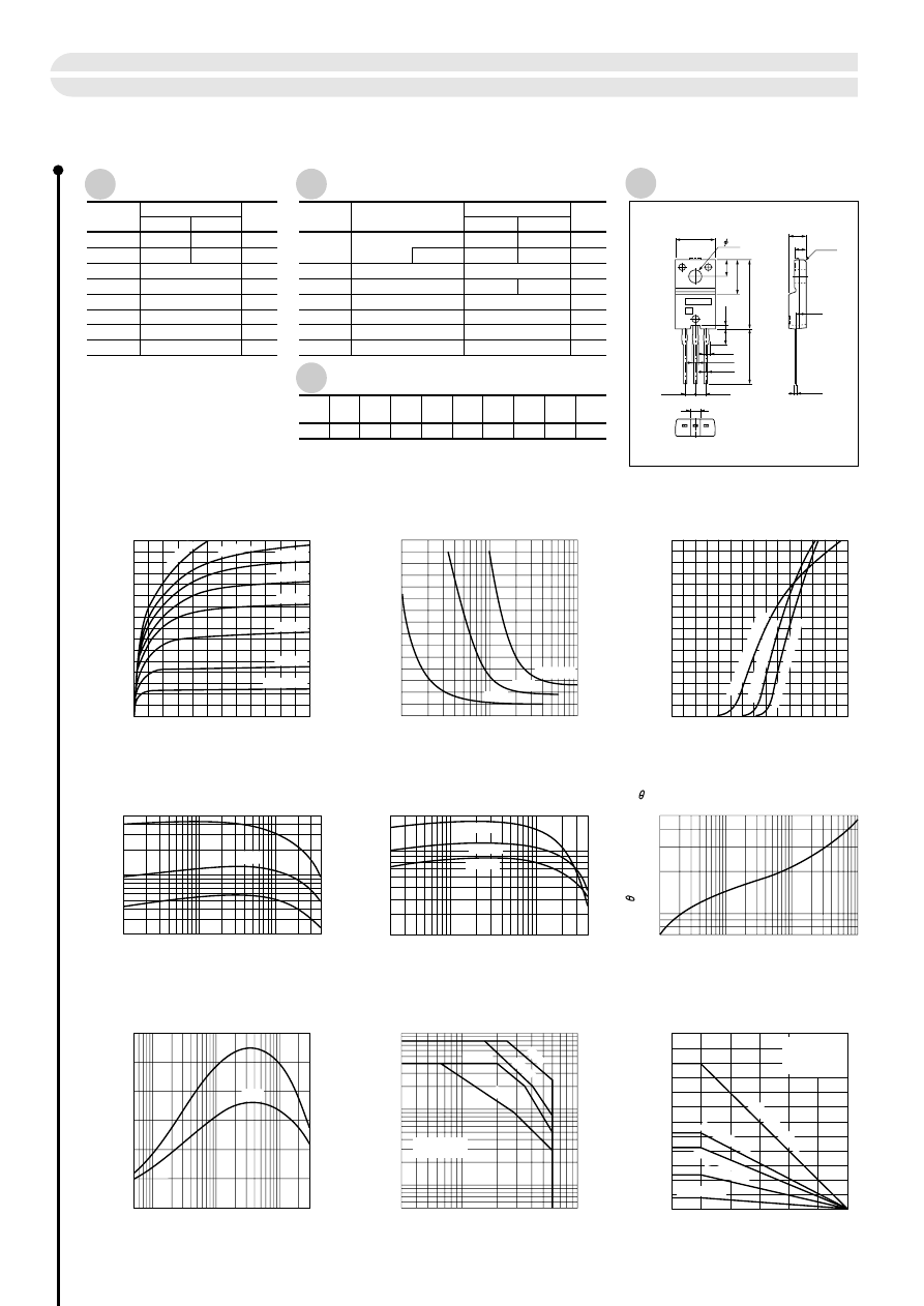
Absolute Maximum Ratings
Electrical Characteristics
Typical Switching Characteristics (common emitter)
Symbol
Ratings
Unit
(Ta=25ºC)
(Ta = 25ºC)
V
CBO
–60
2SA1488
2SA1488A
Symbol
Test Conditions
Ratings
Unit
I
CBO
–12
V
CC
(V)
6
R
L
(
Ω
)
–2
I
C
(A)
–10
V
BB1
(V)
5
V
BB2
(V)
–200
I
B1
(mA)
200
I
B2
(mA)
0.25typ
t
on
(
µ
s)
0.75typ
t
stg
(
µ
s)
0.25typ
t
f
(
µ
s)
µ
A
V
CB
=
–80
–60
–100max
–100max
2SA1488A
2SA1488
I
EBO
µ
A
V
EB
= –6V
–100max
V
(BR) CEO
V
V
I
C
= –25mA
–60min
–80min
h
FE
V
CE
= –4V, I
C
= –1A
40min
V
CE
(sat)
V
I
C
= –2A, I
B
= –0.2A
–0.5max
f
T
MHz
V
CE
= –12V, I
E
= –0.2A
15typ
C
OB
pF
V
CB
= –10V, f = 1MHz
90typ
V
CEO
V
V
–60
–80
–80
V
EBO
V
–6
I
C
A
–4
I
B
A
–1
P
C
W
25 (Tc = 25ºC)
Tj
ºC
150
Tstg
ºC
–55 to +150
■
I
C
—V
CE
Characteristics (typ.)
■
P
C
—Ta Derating
■
I
C
—V
BE
Temperature Characteristics (typ.)
■
h
FE
—I
C
Characteristics (typ.)
■
h
FE
—I
C
Temperature Characteristics (typ.)
■
f
T
—I
E
Characteristics (typ.)
■
j-a
—t Characteristics
■
Safe Operating Area (single pulse)
■
V
CE
(sat)—I
B
Characteristics (typ.)
Power Transistor 2SA1488/1488A
66
–30mA
–40mA
–50mA
–60mA
–20mA
–10mA
I
B
= –5mA
–80mA
0 . 7
1
5
30
20
10
2
0
0
25
50
75
100
125
150
With infinite heatsink
Without heatsink
10
50
100
3
5
–1
–0.5
–0.05
–0.1
–10
–5
Without heatsink
natural air cooling
20
50
100
500
T y p
1m
s
10ms
100ms
DC
150
• 150
• 2
100
• 100
• 2
50 • 50
• 2
20
50
100
200
125ºC
25ºC
–30ºC
0.005 0.01
0.05
0.5
0.1
1
3
0
10
20
30
60
50
40
Typ
0
0
–4
–3
–2
–1
–6
–0.01
–0.05
–0.1
–0.5
–1
–5
–4
–3
–2
–1
V
CE
(V)
I
C
(A)
–0.5
–1.0
–1.5
0
I
B
(A)
V
CE
(sat)
(V)
–1A
–2A
I
C
= –3A
0
–1
–2
–3
–4
0
–0.5
–1.0
–1.5
V
BE
(V)
I
C
(A)
( V
C E
= –4 V )
125
ºC (Case temperature)
25
º
C
(Case temperature)
–
30
º
C (Case temperature)
1
10
100
1000
t (ms)
j-a
(
ºC/
W)
( V
C E
= –4 V )
( V
C E
= –4 V )
–0.02
–0.01
–0.1
–0.5
–1
–4
–0.1
–1
–4
I
C
(A)
I
C
(A)
h
FE
h
FE
f
T
(MHz)
(V
CE
= –12V)
I
E
(A)
V
CE
(V)
I
C
(A)
Ta (ºC)
P
C
(W)
natural air cooling
Silicone grease
Aluminum heatsink
Unit: mm
a) Part No.
b) Lot No.
(Unit: mm)
External Dimensions
TO220F (full-mold)
B C E
C 0.5
16.9
(13.5)
8.4
0.8
3.9
4
10.0
2.6
4.2
2.8
1.35
1.35
0.85
2.54
2.54
0.45
3.3
2.2
a
b
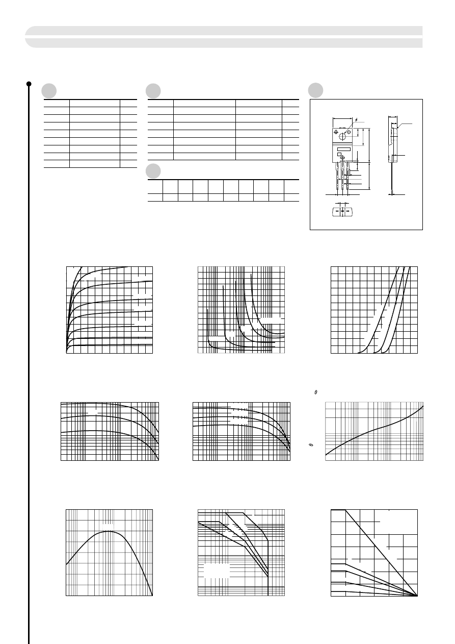
Symbol
Ratings
Unit
(Ta = 25ºC)
(Ta=25ºC)
V
CBO
–50
Symbol
Test Conditions
Ratings
Unit
I
CBO
–24
V
CC
(V)
4
R
L
(
Ω
)
–6
I
C
(A)
–10
V
BB1
(V)
5
V
BB2
(V)
–120
I
B1
(mA)
120
I
B2
(mA)
0.4typ
t
on
(
µ
s)
0.4typ
t
stg
(
µ
s)
0.2typ
t
f
(
µ
s)
µ
A
V
CB
= –50V
–100max
I
EBO
µ
A
V
EB
= –6V
–100max
V
(BR) CEO
V
I
C
= –25mA
–50min
h
FE
V
CE
= –1V, I
C
= –6A
50min
V
CE
(sat)
V
I
C
= –6A, I
B
= –0.3A
–0.35max
f
T
MHz
V
CE
= –12V, I
E
= –0.5A
40typ
C
OB
pF
V
CB
= –10V, f = 1MHz
330typ
V
CEO
V
V
–50
V
EBO
V
–6
I
C
A
–12
I
B
A
–3
P
C
W
35 (Tc = 25ºC)
Tj
ºC
150
Tstg
ºC
–55 to +150
Absolute Maximum Ratings
Electrical Characteristics
Typical Switching Characteristics (common emitter)
■
I
C
—V
CE
Characteristics (typ.)
■
P
C
—Ta Derating
■
I
C
—V
BE
Temperature Characteristics (typ.)
■
h
FE
—I
C
Characteristics (typ.)
■
h
FE
—I
C
Temperature Characteristics (typ.)
■
f
T
—I
E
Characteristics (typ.)
■
j-a
—t Characteristics
■
Safe Operating Area (single pulse)
■
V
CE
(sat)—I
B
Characteristics (typ.)
Power Transistor 2SA1567
67
0
0
–8
–4
–12
–6
–2
–10
–2
–1
–3
–4
–5
–6
V
CE
(V)
I
C
(A)
–40mA
–60mA
–100mA
–150m
A
–20mA
–10mA
–5mA
–
200mA
–10
–50
–100
–3
–5
–1
–0.5
–0.05
–0.1
–30
–10
–5
V
CE
(V)
I
C
(A)
Without heatsink
natural air cooling
0
–1.5
–1.0
–0.5
–2
–100
–10
–1000 –3000
I
B
(mA)
V
CE
(sat)
(V)
–0.02
–0.1
–1
–10
30
50
100
500
I
C
(A)
h
FE
( V
C E
= –1 V )
Typ
1m
s
10ms
100ms
DC
0.3
0.5
4
1
1
10
100
1000
t (ms)
j-a
(
ºC/
W)
0.05 0.1
1
1 2
0
20
30
40
50
f
T
(MHz)
(V
CE
= –12V)
I
E
(A)
Typ
0
–12
–6
–8
–10
–4
–2
0
–1.2
–0.4
–0.2
–0.6
–0.8
–1.0
V
BE
(V)
I
C
(A)
( V
C E
= –4 V )
125
ºC (Case temperature)
25
º
C (Case temperature)
–
30
º
C (Case temperature)
( V
C E
= –1 V )
–0.02
–0.1
–1
–10
30
50
100
500
I
C
(A)
h
FE
125ºC
25ºC
– 30ºC
35
30
20
10
2
0
0
25
50
75
100
125
150
Ta (ºC)
P
C
(W)
W
ith
in
fin
ite
h
e
a
ts
in
k
Without heatsink
50 • 50 • 2
100
• 100
• 2
150
• 150
• 2
–1A
–3A
–6A
–9A
I
C
= –12A
I
B
=
natural air cooling
Silicone grease
Aluminum heatsink
Unit: mm
External Dimensions
TO220F (full-mold)
a) Part No.
b) Lot No.
(Unit: mm)
B C E
C 0.5
16.9
(13.5)
8.4
0.8
3.9
4
10.0
2.2
2.6
4.2
2.8
1.35
1.35
0.85
2.54
2.54
0.45
3.3
a
b
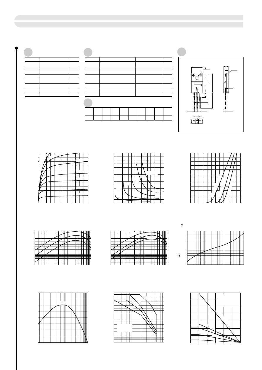
Symbol
Ratings
Unit
(Ta=25ºC)
(Ta=25ºC)
V
CBO
–60
Symbol
Test Conditions
Ratings
Unit
I
CBO
–24
V
CC
(V)
4
R
L
(
Ω
)
–6
I
C
(A)
–10
V
BB1
(V)
5
V
BB2
(V)
–120
I
B1
(mA)
120
I
B2
(mA)
0.4typ
t
on
(
µ
s)
0.4typ
t
stg
(
µ
s)
0.2typ
t
f
(
µ
s)
µ
A
V
CB
= –60V
–100max
I
EBO
mA
V
EB
= –6V
–60max
V
(BR) CEO
V
I
C
= –25mA
–60min
h
FE
V
CE
= –1V, I
C
= –6A
50min
V
CE
(sat)
V
V
I
C
= –6A, I
B
= –0.3A
–0.35max
V
FEC
I
ECO
= –10A
–2.5max
f
T
MHz
V
CE
= –12V, I
E
= 0.5A
40typ
C
OB
pF
V
CB
= –10V, f = 1MHz
330typ
V
CEO
V
V
–60
V
EBO
V
–6
I
C
A
I
B
A
–3
P
C
W
35 (Tc=25ºC)
Tj
ºC
150
Tstg
ºC
–55 to +150
12
±
Absolute Maximum Ratings
Electrical Characteristics
Typical Switching Characteristics (common emitter)
■
I
C
— V
CE
Characteristics (typ.)
■
P
C
— Ta Derating
■
I
C
— V
BE
Temperature Characteristics (typ.)
■
h
FE
— I
C
Characteristics (typ.)
■
h
FE
— I
C
Temperature Characteristics (typ.)
■
f
T
— I
E
Characteristics (typ.)
■
j-a
— t Characteristics
■
Safe Operating Area (single pulse)
■
V
CE
(sat) — I
B
Characteristics (typ.)
Power Transistor 2SA1568
68
0
0
–8
–4
–12
–6
–2
–10
–2
–1
–3
–4
–5
–6
–40mA
–60mA
–100mA
–150mA
–20mA
–10mA
I
B
=
–
200mA
–10
–50
–100
–3
–5
–1
–0.5
–0.05
–0.1
–30
–10
–5
Without heatsink
natural air cooling
0
–1.4
–1.0
–0.5
–7
–100
–10
–1000 –3000
–0.02
–0.1
–1
–12
–10
2
10
300
100
Typ
–0.02
–0.1
–1
–12
–10
2
10
300
100
1m
s
10ms
100ms
DC
0.3
0.5
4
1
1
10
100
1000
0.05 0.1
1
10
0
20
30
50
40
Typ
35
30
20
10
2
0
0
25
50
75
100
125
150
W
ith
in
fin
ite
h
e
a
ts
in
k
Without heatsink
50
• 50 • 2
100
• 100
• 2
150
• 150
• 2
0
–12
–6
–8
–10
–4
–2
0
–1.2
–0.4
–0.2
–0.6
–0.8
–1.0
125ºC
25ºC
–30ºC
V
CE
(V)
I
C
(A)
I
B
(mA)
V
CE
(sat)
(V)
–1A
–3A
–6A
–9A
I
C
= –12A
V
BE
(V)
I
C
(A)
( V
C E
= –1 V )
125
ºC (Case temperature)
25
º
C (Case temperature)
–
30
º
C (Case temperature)
t (ms)
j-a
(º
C/
W)
( V
C E
= –1 V )
I
C
(A)
h
FE
I
C
(A)
h
FE
( V
C E
= –1 V )
f
T
(MHz)
(V
CE
= –12V)
I
E
(A)
V
CE
(V)
I
C
(A)
Ta (ºC)
P
C
(W)
natural air cooling
Silicone grease
Aluminum heatsink
Unit: mm
a) Part No.
b) Lot No.
(Unit : mm)
External Dimensions
TO220F (full-mold)
B C E
C 0.5
16.9
(13.5)
8.4
0.8
3.9
4
10.0
2.2
2.6
4.2
2.8
1.35
1.35
0.85
2.54
2.54
0.45
3.3
a
b
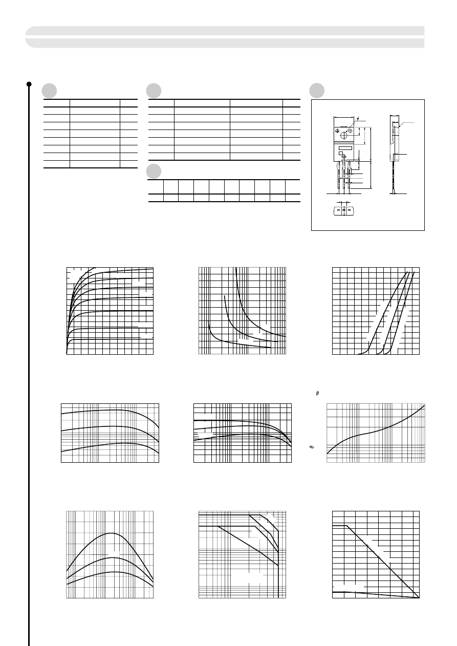
Symbol
Ratings
Unit
(Ta=25ºC)
(Ta=25ºC)
V
CBO
80
Symbol
Test Conditions
Ratings
Unit
I
CBO
12
V
CC
(V)
6
R
L
(
Ω
)
2
I
C
(A)
10
V
BB1
(V)
–5
V
BB2
(V)
200
I
B1
(mA)
–200
I
B2
(mA)
0.2typ
t
on
(
µ
s)
1typ
t
stg
(
µ
s)
0.3typ
t
f
(
µ
s)
I
EBO
µ
A
V
EB
= 6V
100max
µ
A
V
CB
= 80V
100max
V
(BR) CEO
V
I
C
= 25mA
60min
h
FE
V
CE
= 4V, I
C
= 1A
40 to 320
V
CE
(sat)
V
I
C
= 2A, I
B
= 0.2A
0.5max
f
T
MHz
V
CE
= 12V, I
E
= –0.2A
15typ
C
OB
pF
V
CB
= 10V, f = 1MHz
60typ
V
CEO
V
V
60
V
EBO
V
6
I
C
A
4
I
B
A
1
P
C
W
25 (Tc=25ºC)
Tj
ºC
150
Tstg
ºC
–55 to +150
Absolute Maximum Ratings
Electrical Characteristics
Typical Switching Characteristics (common emitter)
■
I
C
— V
CE
Characteristics (typ.)
■
P
C
— Ta Derating
■
I
C
— V
BE
Temperature Characteristics (typ.)
■
h
FE
— I
C
Characteristics (typ.)
■
h
FE
— I
C
Temperature Characteristics (typ.)
■
f
T
— I
E
Characteristics (typ.)
■
j-a
— t Characteristics
■
Safe Operating Area (single pulse)
■
V
CE
(sat) — I
B
Characteristics (typ.)
Power Transistor 2SC3851
69
0
0
1
2
3
4
2
1
3
4
5
6
V
CE
(A)
I
C
(A)
60mA
I
B
=
70mA
50mA
40mA
30mA
20mA
10mA
5mA
30
20
10
0
0
50
100
150
Ta (ºC)
P
C
(W)
W
ith infinite heatsink
W i t h o u t h e a t s i n k
0
1.0
0.5
0.005 0.01
0.1
0.05
1
0.5
I
B
(mA)
V
CE
(sat)
(V)
I
C
=1A
2 A
3 A
0.01
0.1
0.5
1
4
20
50
100
500
I
C
(A)
h
FE
( V
C E
= 4 V )
Typ
0.5
1
5
1
10
100
1000
t (ms)
j-a
(º
C
/W)
10
50
3
5
80
0.05
0.1
1
0.5
10
5
V
CE
(V)
I
C
(A)
W i t h o u t h e a t s i n k
n a t u r a l a i r c o o l i n g
DC
100ms
10ms
1ms
( V
C E
= 4 V )
0.01
0.1
0.05
1
0.5
4
20
50
100
500
I
C
(A)
h
FE
125ºC
0
4
2
3
1
0
1.2
1.0
0.5
V
BE
(V)
I
C
(A)
( V
C E
= 4 V )
125
ºC
(C
ase te
m
p
erature
)
25
º
C (Case temperature)
–
30
º
C
(C
a
se tem
p
erature)
–0.005
–0.1
–0.5 –1
–4
20
10
0
30
40
f
T
(MHz)
I
E
(A)
T y p
–30ºC
25ºC
(V
CE
= 12V)
a) Part No.
b) Lot No.
(Unit : mm)
External Dimensions
TO220F (full-mold)
B C E
C 0.5
16.9
(13.5)
8.4
0.8
3.9
4
10.0
2.2
2.6
4.2
2.8
1.35
1.35
0.85
2.54
2.54
0.45
3.3
a
b
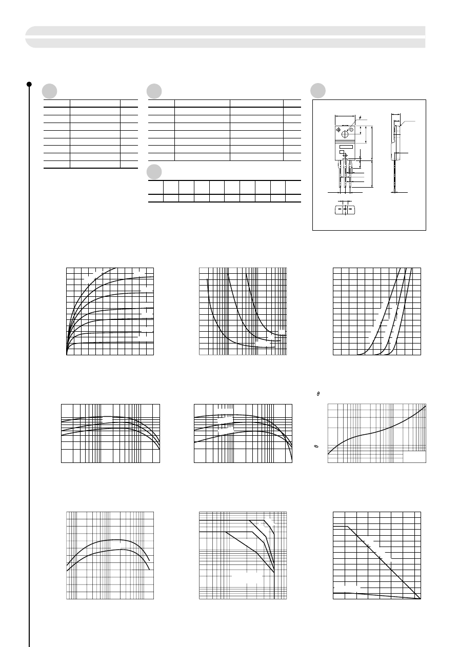
Symbol
Ratings
Unit
(Ta=25ºC)
(Ta=25ºC)
V
CBO
80
Symbol
Test Conditions
Ratings
Unit
20
V
CC
(V)
20
R
L
(
Ω
)
1.0
I
C
(A)
10
V
BB1
(V)
–5
V
BB2
(V)
15
I
B1
(mA)
–30
I
B2
(mA)
0.8typ
t
on
(
µ
s)
3.0typ
t
stg
(
µ
s)
1.2typ
t
f
(
µ
s)
µ
A
10max
I
EBO
µ
A
V
EB
= 6V
I
CBO
V
CB
= 80V
100max
V
(BR) CEO
V
I
C
= 25mA
60min
h
FE
V
CE
= 4V, I
C
= 0.5A
500min
V
CE
(sat)
V
I
C
= 2A, I
B
= 50mA
0.5max
f
T
MHz
V
CE
= 12V, I
E
= –0.2A
15typ
C
OB
pF
V
CB
= 10V, f = 1MHz
50typ
V
CEO
V
V
60
V
EBO
V
6
I
C
A
3
I
B
A
1
P
C
W
25 (Tc=25ºC)
Tj
ºC
150
Tstg
ºC
–55 to +150
Absolute Maximum Ratings
Electrical Characteristics
Typical Switching Characteristics (common emitter)
■
I
C
— V
CE
Characteristics (typ.)
■
P
C
— Ta Derating
■
I
C
— V
BE
Temperature Characteristics (typ.)
■
h
FE
— I
C
Characteristics (typ.)
■
h
FE
— I
C
Temperature Characteristics (typ.)
■
f
T
— I
E
Characteristics (typ.)
■
j-a
— t Characteristics
■
Safe Operating Area (single pulse)
■
V
CE
(sat) — I
B
Characteristics (typ.)
Power Transistor 2SC3852
70
0
0
1
2
3
2
1
3
4
5
6
I
B
=12mA
0.5mA
1mA
2mA
3mA
5mA
8mA
0.01
0.1
0.5
1
3
100
500
2000
1000
(VCE=4V)
Typ
0.01
0.1
0.5
1
3
100
500
2000
1000
0.5
1
5
1
10
100
1000
V
CB
= 10V
I
E
= –2A
10
50
3
5
100
0.05
0.1
1
0.5
10
5
Without heatsink
natural air cooling
DC
100ms
10ms
1ms
0
1.0
1.5
0.5
0.001
0.005 0.01
0.1
0.05
1
0.5
2A
3A
0
2
3
1
0
1.1
1.0
0.5
25ºC
–30ºC
125ºC
–0.005 –0.01
–0.1
–0.5
–0.05
–2
–1
20
10
0
30
Typ
30
20
10
0
0
50
100
150
With infinite heatsink
Without heatsink
V
CE
(V)
I
C
(A)
I
B
(A)
V
CE
(sat)
(V)
I
C
=1A
V
BE
(V)
I
C
(A)
( V
C E
= 4 V )
125
ºC (Case temperature)
25
º
C (Case tem
perature)
–
30
º
C (Case temperature)
t (ms)
j-a
(º
C/
W)
( V
C E
= 4 V )
I
C
(A)
I
C
(A)
h
FE
h
FE
f
T
(MHz)
(V
CE
= 12V)
I
E
(A)
V
CE
(V)
I
C
(A)
Ta (ºC)
P
C
(W)
a) Part No.
b) Lot No.
(Unit : mm)
External Dimensions
TO220F (full-mold)
B C E
C 0.5
16.9
(13.5)
8.4
0.8
3.9
4
10.0
2.2
2.6
4.2
2.8
1.35
1.35
0.85
2.54
2.54
0.45
3.3
a
b

Symbol
Ratings
Unit
(Ta=25ºC)
(Ta=25ºC)
V
CBO
100
Symbol
Test Conditions
Ratings
Unit
I
CBO
20
V
CC
(V)
4
R
L
(
Ω
)
5
I
C
(A)
0.1
I
B1
(A)
–0.1
I
B2
(A)
0.5typ
t
on
(
µ
s)
2.0typ
t
stg
(
µ
s)
0.5typ
t
f
(
µ
s)
µ
A
µ
A
V
CB
= 100V
10max
I
EBO
V
EB
= 15V
10max
V
(BR) CEO
V
I
C
= 25mA
50min
h
FE
V
CE
= 4V, I
C
= 1A
300 to 1600
V
CE
(sat)
V
I
C
= 5A, I
B
= 0.1A
0.5max
f
T
MHz
V
CB
= 12V, I
E
= –0.5A
24typ
C
OB
pF
V
CB
= 10V, f = 1MHz
150typ
V
CEO
V
V
50
V
EBO
V
15
I
C
A
I
B
A
3
P
C
W
35 (Tc=25ºC)
Tj
ºC
150
Tstg
ºC
–55 to +150
10
Absolute Maximum Ratings
Electrical Characteristics
Typical Switching Characteristics (common emitter)
■
I
C
— V
CE
Characteristics (typ.)
■
P
C
— Ta Derating
■
I
C
— V
BE
Temperature Characteristics (typ.)
■
h
FE
— I
C
Characteristics (typ.)
■
h
FE
— I
C
Temperature Characteristics (typ.)
■
f
T
— I
E
Characteristics (typ.)
■
j-a
— t Characteristics
■
Safe Operating Area (single pulse)
■
V
CE
(sat) — I
B
Characteristics (typ.)
Power Transistor 2SC4024
71
0
0
4
2
6
10
8
2
4
6
I
B
= 35mA
5mA
25mA
30mA
10mA
15mA
20mA
0
1.0
1.5
0.5
0.002
0.01
0.1
2
1
0.02
0.1
0.5
5
1
10
100
500
1000
Typ
0.02
0.1
0.5
5
1
10
100
500
1000
10A
0.3
0.5
1
4
1
10
100
1000
10
50
3
5
100
0.2
1
0.5
30
10
5
Without heatsink
natural air cooling
DC
100ms
10ms
1ms
40
30
20
10
2
0
0
25
50
75
100
125
150
With infinite heatsink
Without heatsink
50
• 50 • 2 100 • 100
• 2
0
10
2
4
8
6
0
1.2
1.0
0.5
25ºC
–30º
C
125ºC
–0.05 –0.1
–1
–0.5
–5
–10
20
10
0
30
Typ
V
CE
(V)
I
C
(A)
I
B
(A)
V
CE
(sat)
(V)
I
C
= 1A
3A
5A
V
BE
(V)
I
C
(A)
( V
C E
= 4 V )
1
2
5
ºC
(C
a
se
te
m
p
e
ratu
re
)
25
ºC (Case temperature)
–
30
º
C (Case temperature)
t
(ms)
j-a
(º
C
/W
)
( V
C E
= 4 V )
( V
C E
= 4 V )
I
C
(A)
I
C
(A)
h
FE
h
FE
f
T
(MHz)
(V
CE
= 12V)
I
E
(A)
V
CE
(V)
I
C
(A)
Ta (ºC)
P
C
(W)
150
• 150
• 2
natural air cooling
Silicone grease
Aluminum heatsink
Unit: mm
a) Part No.
b) Lot No.
(Unit: mm)
External Dimensions
TO220F (full-mold)
B C E
C 0.5
16.9
(13.5)
8.4
0.8
3.9
4
10.0
2.2
2.6
4.2
2.8
1.35
1.35
0.85
2.54
2.54
0.45
3.3
a
b
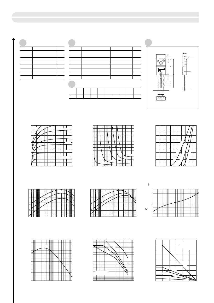
Absolute Maximum Ratings
Electrical Characteristics
Typical Switching Characteristics (common emitter)
Symbol
Ratings
Unit
(Ta=25ºC)
(Ta=25ºC)
V
CBO
60
Symbol
Test Conditions
Ratings
Unit
I
CBO
24
V
CC
(V)
4
R
L
(
Ω
)
6
I
C
(A)
10
V
BB1
(V)
–5
V
BB2
(V)
0.12
I
B1
(A)
–0.12
I
B2
(A)
0.6typ
t
on
(
µ
s)
1.4typ
t
stg
(
µ
s)
0.4typ
t
f
(
µ
s)
µ
A
V
CB
= 60V
100max
I
EBO
mA
V
EB
= 6V
60max
V
(BR) CEO
V
I
C
= 25mA
60min
h
FE
V
CE
= 1V, I
C
= 6A
50min
V
CE
(sat)
V
V
I
C
= 6A, I
B
= 1.3A
0.35max
V
FEC
V
ECO
= 10A
2.5max
f
T
MHz
V
CE
= 12V, I
E
= –0.5A
24typ
C
OB
pF
V
CB
= 10V, f = 1MHz
180typ
V
CEO
V
V
60
V
EBO
V
6
I
C
A
I
B
A
3
P
C
W
35 (Tc=25ºC)
Tj
ºC
150
Tstg
ºC
–55 to +150
±
12
■
I
C
— V
CE
Characteristics (typ.)
■
P
C
— Ta Derating
■
I
C
— V
BE
Temperature Characteristics (typ.)
■
h
FE
— I
C
Characteristics (typ.)
■
h
FE
— I
C
Temperature Characteristics (typ.)
■
f
T
— I
E
Characteristics (typ.)
■
j-a
— t Characteristics
■
Safe Operating Area (single pulse)
■
V
CE
(sat) — I
B
Characteristics (typ.)
Power Transistor 2SC4065
72
0
0
4
2
8
6
12
10
2
4
6
200mA
I
B
= 10mA
20mA
40mA
60mA
100mA
150m
A
0
1.0
1.3
0.5
0.005 0.01
0.1
3
1
I
C
= 1A
12A
3A
6A
9A
0.02
0.1
1
10 12
3
5
50
10
100
400
Typ
0.02
0.1
1
10 12
3
5
50
10
100
400
0.2
0.5
1
5
1
10
100
1000
10
50
3
5
100
0.05
0.1
1
0.5
30
10
5
Without heatsink
natural air cooling
DC
100ms
10ms
1ms
40
30
20
10
2
0
0
25
50
75
100
125
150
With infinite heatsink
Without heatsink
50 • 50 • 2 100 • 100
• 2
0
12
10
2
4
8
6
0
1.1
1.0
0.5
25
ºC
–30
ºC
125
ºC
–0.05 –0.1
–1
–0.5
–5
–12
–10
20
10
0
30
Typ
V
CE
(V)
I
C
(A)
I
B
(A)
V
CE
(sat)
(V)
V
BE
(V)
I
C
(A)
( V
C E
= 1 V )
25
º
C
(Case temperature)
125
ºC (Case temperature)
–
30
º
C
(Case temperature)
t (ms)
j-a
(º
C/
W)
(V
CE
= 1V)
(V
CE
= 1V)
I
C
(A)
I
C
(A)
h
FE
h
FE
f
T
(MHz)
(V
CE
= 12V)
I
E
(A)
V
CE
(V)
I
C
(A)
natural air cooling
Silicone grease
Aluminum heatsink
Unit: mm
Ta
(ºC)
P
C
(W)
150
• 150
• 2
a) Part No.
b) Lot No.
(Unit: mm)
External Dimensions
TO220F (full-mold)
B C E
C 0.5
16.9
(13.5)
8.4
0.8
3.9
4
10.0
2.2
2.6
4.2
2.8
1.35
1.35
0.85
2.54
2.54
0.45
3.3
a
b
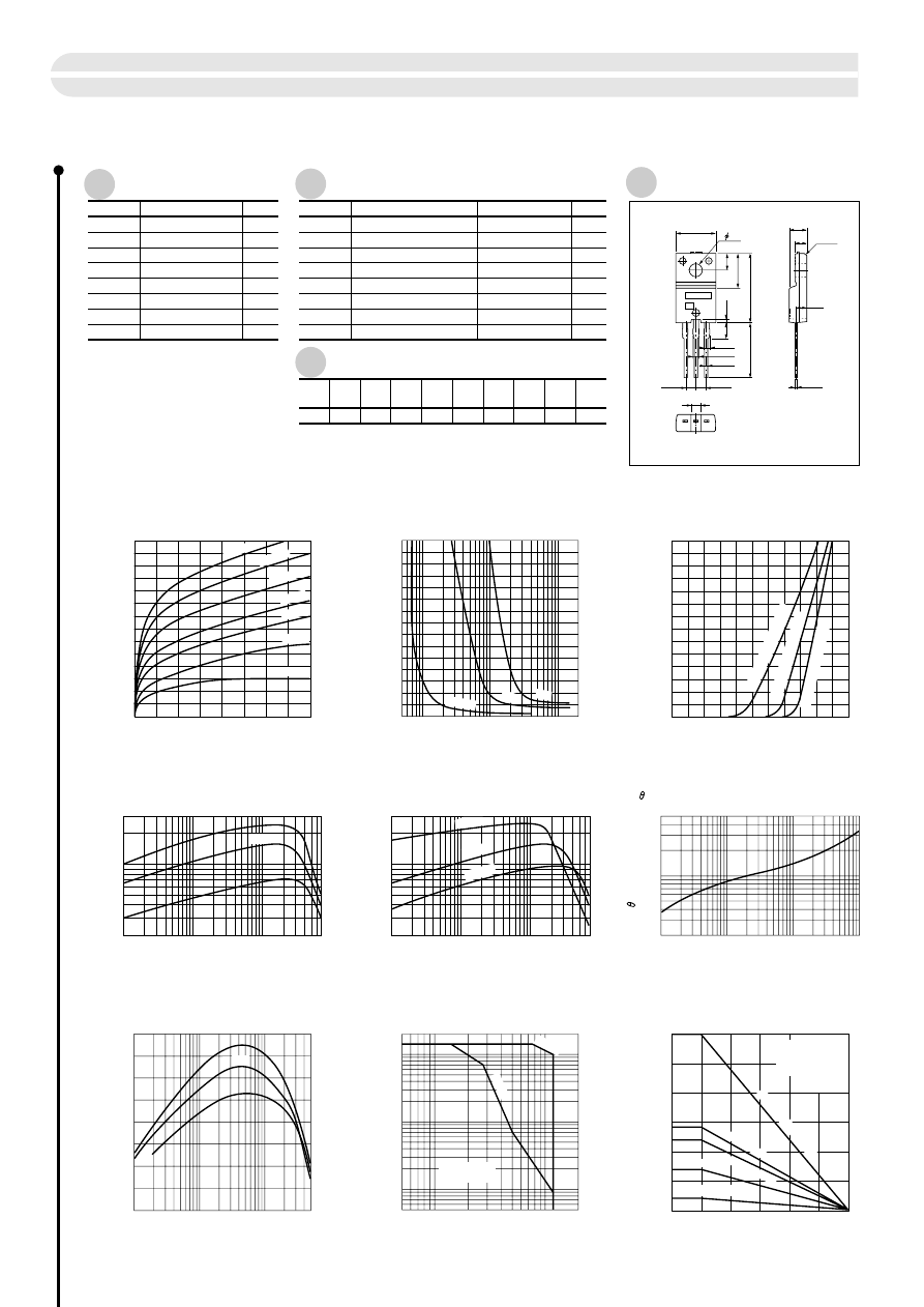
Symbol
Ratings
Unit
(Ta=25ºC)
(Ta =25ºC)
V
CBO
200
Symbol
Test Conditions
Ratings
Unit
I
CBO
50
V
CC
(V)
16.7
R
L
(
Ω
)
3
I
C
(A)
10
V
BB1
(V)
–5
V
BB2
(V)
0.3
I
B1
(A)
–0.6
I
B2
(A)
0.5max
t
on
(
µ
s)
3max
t
stg
(
µ
s)
0.5max
t
f
(
µ
s)
µ
A
V
CB
= 200V
100max
I
EBO
µ
A
V
EB
= 8V
100max
V
(BR) CEO
V
I
C
= 50mA
120min
h
FE
V
CE
= 4V, I
C
= 3A
70 to 220
V
CE (sat)
V
V
I
C
= 3A, I
B
= 0.3A
0.5max
V
BE (sat)
I
C
= 3A, I
B
= 0.3A
1.2max
f
T
MHz
V
CE
= 12V, I
E
= –0.5A
30typ
C
OB
pF
V
CB
= 10V, f = 1MHz
110typ
V
CEO
V
V
120
V
EBO
V
8
I
C
A
I
B
A
3
P
C
W
30 (Tc=25ºC)
Tj
ºC
150
Tstg
ºC
–55 to +150
7 (pulse 14)
Absolute Maximum Ratings
Electrical Characteristics
Typical Switching Characteristics (common emitter)
■
I
C
— V
CE
Characteristics (typ.)
■
P
C
— Ta Derating
■
I
C
— V
BE
Temperature Characteristics (typ.)
■
h
FE
— I
C
Characteristics (typ.)
■
h
FE
— I
C
Temperature Characteristics (typ.)
■
f
T
— I
E
Characteristics (typ.)
■
Safe Operating Area (single pulse)
■
V
CE
(sat) — I
B
Characteristics (typ.)
Power Transistor 2SC4153
73
0
0
3
4
2
1
5
7
5
2
1
3
4
200m
A
150mA
100mA
I
B
=10mA
20mA
40mA
60mA
0
2
3
1
0.005 0.01
0.1
2
1
I
C
= 1A
3A
5A
0.01
0.1
0.5
1
7
5
20
50
100
300
(V
CE
= 4V)
Typ
0.01
0.1
0.5
1
7
5
20
50
100
300
0.2
0.5
1
5
1
10
100
1000
–0.01
–0.1
–1
–5
0
10
20
40
30
Typ
10
100
50
5
200
0.05
1
0.5
0.1
20
10
5
Without heatsink
natural air cooling
100
µ
s
10ms
30
20
10
2
0
0
25
50
75
100
125
150
W
ith infinite heatsink
Without heatsink
0
7
2
3
4
5
6
1
0
1.1
1.0
0.5
25ºC
–30º
C
125ºC
V
CE
(V)
I
C
(A)
I
B
(A)
V
CE
(sat)
(V)
V
BE
(V)
I
C
(A)
( V
C E
= 4 V )
25
º
C (Case temperature)
125
ºC
(Case temperature)
–
3
0
º
C
(C
a
s
e
te
m
p
e
ra
tu
re
)
t (ms)
(V
CE
= 4V)
I
C
(A)
I
C
(A)
h
FE
h
FE
f
T
(MHz)
(V
CE
= 12V)
I
E
(A)
V
CE
(V)
I
C
(A)
natural air cooling
Silicone grease
Aluminum heatsink
Unit: mm
Ta (ºC)
P
C
(W)
50 • 50 • 2
100
• 100
• 2
150
• 150
• 2
a) Part No.
b) Lot No.
(Unit: mm)
External Dimensions
TO220F (full-mold)
B C E
C 0.5
16.9
(13.5)
8.4
0.8
3.9
4
10.0
2.2
2.6
4.2
2.8
1.35
1.35
0.85
2.54
2.54
0.45
3.3
a
b
■
j-a
— t Characteristics
j-a
(º
C/
W)
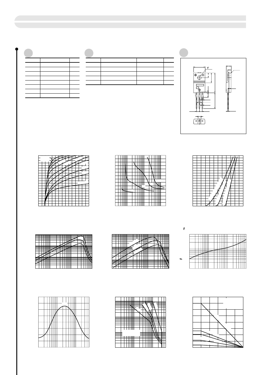
Absolute Maximum Ratings
Electrical Characteristics
Symbol
Ratings
Unit
(Ta=25ºC)
(Ta=25ºC)
V
CBO
380
±
50
Symbol
Test Conditions
Ratings
Unit
I
CBO
µ
A
V
CB
= 330V
10max
I
EBO
µ
A
V
EB
= 6V
20max
V
(BR) CEO
V
I
C
= 25mA
h
FE
V
CE
= 2V, I
C
= 3A
330 to 430
V
CE (
sat
)
V
I
C
= 4A, I
B
= 20mA
1.5max
1500min
V
CEO
V
V
380
±
50
V
EBO
V
6
I
C
A
I
B
A
1
P
C
W
35 (Tc=25ºC)
Tj
ºC
150
Tstg
ºC
–55 to +150
6 (pulse 10)
■
I
C
— V
CE
Characteristics (typ.)
■
P
C
— Ta Derating
■
I
C
— V
BE
Temperature Characteristics (typ.)
■
h
FE
— I
C
Characteristics (typ.)
■
h
FE
— I
C
Temperature Characteristics (typ.)
■
f
T
— I
E
Characteristics (typ.)
■
j-a
— t Characteristics
■
Safe Operating Area (single pulse)
■
V
CE
(sat) — I
B
Characteristics (typ.)
Power Transistor 2SD2141
74
0
0
5
10
2
4
6
I
B
= 1mA
2mA
4mA
18mA
20mA
90mA
60mA
0
3
2
1
0.2
1
0.5
10
5
200
100
50
1A
3A
5A
I
C
= 7A
0.02
0.1
1
0.5
10
5
5000
10000
1000
500
100
10
50
Typ
0.1
1
5
0.5
1
10
100
1000
1ms
10m
s
100ms
50
10
5
1
100
500
0.01
0.05
0.1
1
0.5
10
20
5
DC
Without heatsink
natural air cooling
40
30
20
10
2
0
0
25
50
75
100
125
150
W
ith infinite heatsink
Without heatsink
0
10
5
0
2.0
2.4
1.0
0.02
0.1
1.0
5
0.5
10
5000
10000
1000
500
100
50
20
125
ºC
–55
ºC
25
ºC
–0.05
–0.01
–0.1
–0.5 –1
–5
0
20
10
30
40
Typ
V
CE
(V)
I
C
(A)
120mA
150mA
I
B
(mA)
V
CE
(sat)
(V)
V
BE
(V)
I
C
(A)
( V
C E
= 4 V )
25
ºC (C
ase tem
perature)
125
ºC (Case temperature)
–
3
0
º
C
(C
a
s
e
te
m
p
e
ra
tu
re
)
t
(ms)
j-a
(º
C/
W)
(V
CE
= 2V)
(V
CE
= 2V)
I
C
(A)
I
C
(A)
h
FE
h
FE
f
T
(MHz)
(V
CE
= 12V)
I
E
(A)
V
CE
(V)
I
C
(A)
natural air cooling
Silicone grease
Aluminum heatsink
Unit: mm
Ta
(ºC)
P
C
(W)
100
• 100
• 2
150
• 150
• 2
50 • 50 • 2
a) Part No.
b) Lot No.
(Unit: mm)
External Dimensions
TO220F (full-mold)
B C E
C 0.5
16.9
(13.5)
8.4
0.8
3.9
4
10.0
2.2
2.6
4.2
2.8
1.35
1.35
0.85
2.54
2.54
0.45
3.3
a
b
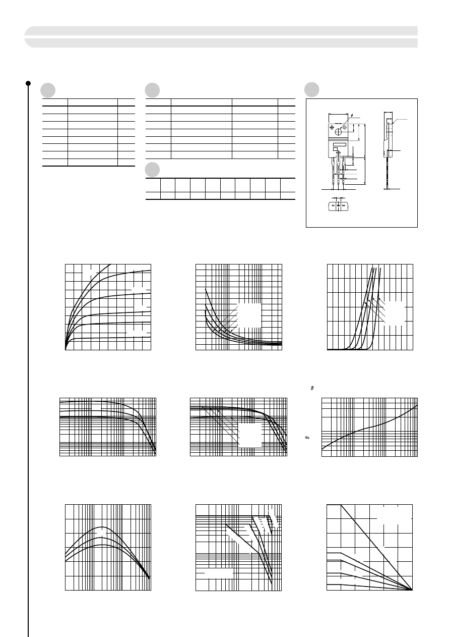
Symbol
Ratings
Unit
(Ta=25ºC)
(Ta=25ºC)
V
CBO
V
65
±
5
Symbol
Test Conditions
Ratings
Unit
I
CBO
12
V
CC
(V)
12
R
L
(
Ω
)
1
I
C
(A)
10
V
BB1
(V)
–5
V
BB2
(V)
30
I
B1
(mA)
–30
I
B2
(mA)
0.25
t
on
(
µ
s)
0.8
t
stg
(
µ
s)
0.35
t
f
(
µ
s)
µ
A
V
CB
= 60V
10max
I
EBO
µ
A
V
EB
= 6V
10max
V
CEO
V
I
C
= 50mA
60 to 70
h
FE
V
CE
= 1V, I
C
= 1A
700 to 3000
V
CE
(sat)
V
I
C
= 1.5A, I
B
= 15mA
0.15max
V
FEC
V
I
FEC
= 6A
1.5max
Es/b
mJ
L = 10mH, single pulse
200min
V
CEO
V
65
±
5
V
EBO
V
6
I
C
A
±
6 (pulse
±
10)
I
B
A
1
P
C
W
30 (Tc=25ºC)
Tj
ºC
150
Tstg
ºC
–55 to +150
0
1
2
3
4
5
■
I
C
— V
CE
Characteristics (typ.)
■
P
C
— Ta Derating
■
I
C
— V
BE
Temperature Characteristics (typ.)
0
10
8
6
4
2
I
C
(A
)
V
CE
(V)
0.01
0.05 0.1
1
0.5
5
10
■
h
FE
— I
C
Characteristics (typ.)
5000
1000
500
100
50
30
h
FE
I
C
(A)
(V
CE
= 1V)
0.01
0.05 0.1
1
0.5
5
10
■
h
FE
— I
C
Temperature Characteristics (typ.)
5000
1000
500
100
50
30
h
FE
I
C
(A)
(V
CE
= 1V)
–0.01
–0.05 –0.1
–1
–0.5
–5 –10
■
f
T
— I
E
Characteristics (typ.)
30
25
20
15
10
5
0
f
T
(
MHz
)
I
E
(A)
1
5
10
100
50
500 1000
■
j-a
— t Characteristics
5
1
0.5
0.3
j-a
(
ºC/
W)
t (ms)
(V
CE
= 1V)
(I
C
= 1.5A)
0
50
100
150
0
30
20
10
P
C
(
W
)
Ta (
ºC)
■
Safe Operating Area (single pulse)
1
5
10
50
100
20
10
1
0.1
0.5
5
I
C
(A
)
V
CE
(V)
0
0.5
1.0
1.5
0
6
4
5
2
1
3
I
C
(A
)
V
BE
(V)
■
V
CE
(sat) — I
B
Temperature Characteristics (typ.)
1
5
10
50 100
400
0
0.75
0.5
0.25
V
CE
(sat)
(V
)
I
B
(mA)
I
B
= 1mA
3mA
5mA
10mA
20mA
30mA
natural air cooling
Silicone grease
Aluminum heatsink
Unit: mm
50 • 50
• 2
100
• 100
• 2
150
• 1
50 • 2
Without heatsink
W
ith
in
fin
ite
h
e
a
ts
in
k
Ta=55ºC
25ºC
75ºC
125ºC
Ta = –55ºC
25ºC
75ºC
125ºC
Without heatsink
natural air cooling
0.5
msec
1msec
10
msec
100
msec
D.C (Tc
= 2
5ºC)
Ta = –55ºC
25ºC
75ºC
125ºC
Typ
Absolute Maximum Ratings
Electrical Characteristics
Typical Switching Characteristics
Power Transistor 2SD2382
75
Typ
a) Part No.
b) Lot No.
(Unit: mm)
External Dimensions
TO220F (full-mold)
B C E
C 0.5
16.9
(13.5)
8.4
0.8
3.9
4
10.0
2.2
2.6
4.2
2.8
1.35
1.35
0.85
2.54
2.54
0.45
3.3
a
b
Absolute Maximum Ratings
Electrical Characteristics
Symbol
Ratings
Unit
(Ta=25ºC)
(Ta=25ºC)
V
CBO
200
Symbol
Test Conditions
Ratings
Unit
I
CBO
µ
A
V
CB
=200V
100max
I
EBO
mA
V
EB
=6V
10max
V
CEO
V
I
C
=50mA
h
FE
V
CE
=2V, I
C
=6A
150min
V
BE
(sat)
V
I
C
=6A, I
B
=6mA
2.0max
V
CE
(sat)
V
I
C
=6A, I
B
=6mA
1.5max
2000min
V
CEO
V
V
150
V
EBO
V
6
8
I
C
A
I
B
A
1
P
C
W
35 (Tc=25ºC)
2 (Ta=25ºC, No Fin)
Tj
ºC
150
Tstg
ºC
–55 to +150
Power Transistor 2SD2633
76
External Dimensions
TO220F (full-mold)
B C E
C 0.5
16.9
(13.5)
8.4
0.8
3.9
4
10.0
2.2
2.6
4.2
2.8
1.35
1.35
0.85
2.54
2.54
0.45
3.3
a
b
a) Part No.
b) Lot No.
(Unit: mm)
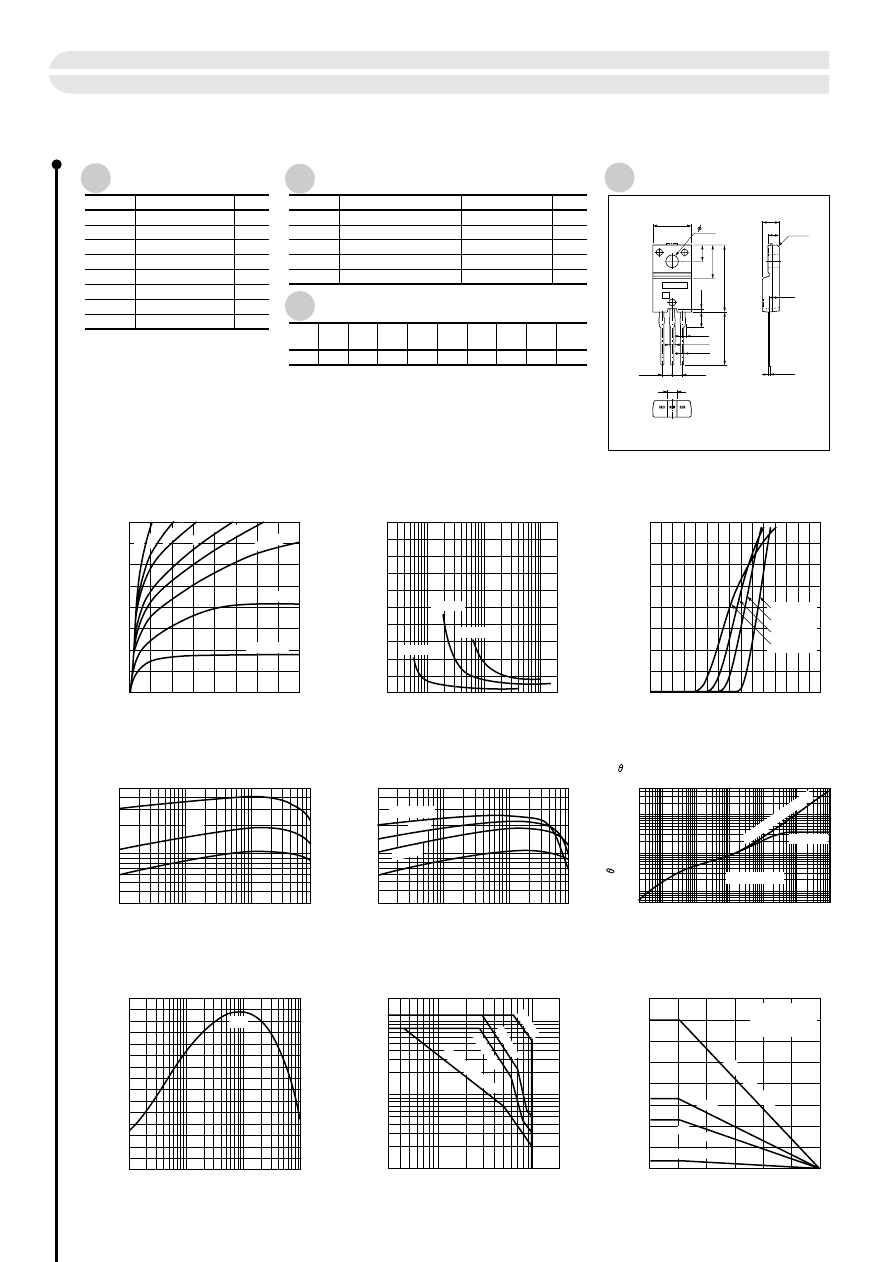
Absolute Maximum Ratings
Electrical Characteristics
Typical Switching Characteristics
0
1
2
3
4
0
8
6
4
2
I
C
(A)
V
CE
(V)
0.01
0.05 0.1
1
0.5
5
8
500
100
30
50
h
FE
I
C
(A)
(V
CE
= 4V)
0.01
0.05 0.1
1
0.5
5 8
500
100
50
30
h
FE
I
C
(A)
(V
CE
= 4V)
–0.01
–0.05 –0.1
–1
–0.5
–5 –10
30
20
10
0
f
T
(MHz
)
I
E
(A)
0.0002
0.01
0.001
0.1
1
10
100
50
10
1
5
0.1
0.5
0.05
j-a
(
ºC/
W
)
t (sec)
(V
CE
= 12V)
0
50
100
150
0
40
30
20
10
P
C
(W)
Ta (
ºC)
3
5
10
50
200
100
20
10
1
0.1
0.5
5
I
C
(A)
V
CE
(V)
0
0.5
1.0
1.5
0
8
6
2
4
I
C
(A)
V
BE
(V)
5
10
50 100
500
2000
1000
0
2
1
V
CE
(sat)
(V)
I
B
(mA)
I
B
= 10mA
25mA
50mA
natural air cooling
Silicone grease
Aluminum heatsink
Unit: mm
100
• 100
• 2
200
• 200
• 2
Without heatsink
W
ith
in
fin
ite
h
ea
tsin
k
Tc = –55ºC
25ºC
75ºC
125ºC
Ic = 1A
Ic = 3A
Ic = 5A
1msec
10
msec
100
msec
D.C (Tc
= 2
5ºC)
Tc = 125ºC
75ºC
25ºC
–55ºC
Typ
75m
A
100mA
150m
A
200mA
300m
A
Ta = 25ºC
Single Pulese
NO FIN (Ta
=
25
ºC)
Symbol
Ratings
Unit
(Ta=25ºC)
(Ta=25ºC)
V
CBO
120
Symbol
Test Conditions
Ratings
Unit
I
CBO
12
V
CC
(V)
4
R
L
(
Ω
)
3
I
C
(A)
10
V
BB1
(V)
–5
V
BB2
(V)
30
I
B1
(mA)
–30
I
B2
(mA)
1.0
t
on
(
µ
s)
2.0
t
stg
(
µ
s)
0.5
t
f
(
µ
s)
µ
A
V
CB
= 120V
10max
I
EBO
µ
A
V
EB
= 6V
10max
V
CEO
V
I
C
= 50mA
100min
h
FE
V
CE
= 4V, I
C
= 3A
70min
V
CE
(sat)
V
I
C
= 4A, I
B
= 0.4A
0.3max
V
CEO
V
V
100
V
EBO
V
6
I
C
A
8 (pulse 12)
I
B
A
3
P
C
W
35 (Tc=25ºC)
Tj
ºC
150
Tstg
ºC
–55 to +150
■
I
C
— V
CE
Characteristics (typ.)
■
P
C
— Ta Derating
■
I
C
— V
BE
Temperature Characteristics (typ.)
■
h
FE
— I
C
Characteristics (typ.)
■
h
FE
— I
C
Temperature Characteristics (typ.)
■
f
T
— I
E
Characteristics (typ.)
■
j-a
— t Characteristics
■
Safe Operating Area (single pulse)
■
V
CE
(sat) — I
B
Characteristics (typ.)
Power Transistor FN812
77
Typ
a) Part No.
b) Lot No.
(Unit: mm)
External Dimensions
TO220F (full-mold)
B C E
C 0.5
16.9
(13.5)
8.4
0.8
3.9
4
10.0
2.2
2.6
4.2
2.8
1.35
1.35
0.85
2.54
2.54
0.45
3.3
a
b
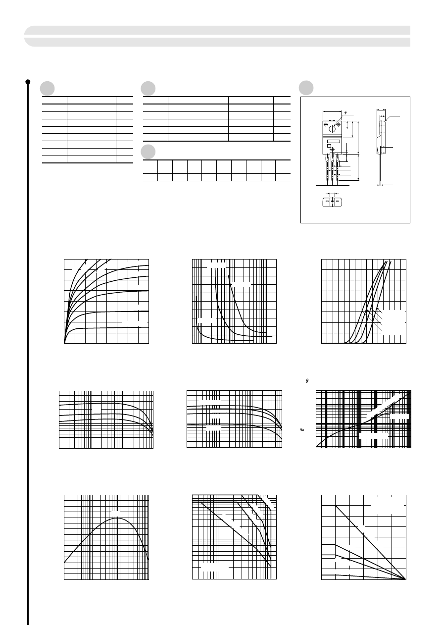
0
–
1
–
2
–
3
–
4
–
8
–
6
–
4
–
2
0
I
C
(A)
V
CE
(V)
–
0.01
–
0.05 –0.1
–
1
–
0.5
–
5 –8
500
100
30
50
h
FE
I
C
(A)
(V
CE
= –4V)
0.01
0.05 0.1
1
0.5
5
10
30
20
10
0
f
T
(MHz
)
I
E
(A)
0.0002
0.01
0.001
0.1
1
10
100
50
10
1
5
0.1
0.5
0.05
j-a
(
ºC/
W
)
t (sec)
(V
CE
= 12V)
0
50
100
150
0
40
30
20
10
P
C
(W)
Ta (
ºC)
–3
–5
–10
–50
–150
–100
–12
–10
–1
–0.1
–0.5
–5
I
C
(A)
V
CE
(V)
0
–0.5
–1.0
–1.5
0
–8
–6
–2
–4
I
C
(A)
V
BE
(V)
–5
–10
–50
–100
–500
–2000
–1000
0
–2
–1
V
CE
(sat)
(A)
I
B
(mA)
I
B
= –10mA
–
25mA
–
50mA
natural air cooling
Silicone grease
Aluminum heatsink
Unit: mm
100
•100
• 2
200
•200
•2
Without heatsink
W
ith
in
fin
ite
h
eatsink
Tc = –40ºC
25ºC
75ºC
125ºC
Ic = –1A
Ic = –3A
Ic = –5A
1m
sec
10
msec
100
msec
D.C (Tc
= 2
5ºC)
Typ
–75mA
–100mA
–150mA
–200m
A
–300mA
Tc = 25ºC
Single Pulese
NO Fin (Ta
=
25
ºC)
(V
BE
= –4V)
natural air cooling
Without heatsink
Symbol
Ratings
Unit
(Ta=25ºC)
(Ta=25ºC)
V
CBO
–120
Symbol
Test Conditions
Ratings
Unit
I
CBO
–12
V
CC
(V)
4
R
L
(
Ω
)
–3
I
C
(A)
–10
V
BB1
(V)
5
V
BB2
(V)
–30
I
B1
(mA)
30
I
B2
(mA)
2.5
t
on
(
µ
s)
0.4
t
stg
(
µ
s)
0.6
t
f
(
µ
s)
µ
A
V
CB
= –120V
10max
I
EBO
µ
A
V
EB
= –6V
10max
V
CEO
V
I
C
= –50mA
–120min
h
FE
V
CE
= –4V, I
C
= –3A
70min
V
CE
(sat)
V
I
C
= –3A, I
B
= –0.3A
–0.3max
V
CEO
V
V
–120
V
EBO
V
–6
I
C
A
–8 (pulse –12)
I
B
A
–3
P
C
W
35 (Tc=25ºC)
Tj
ºC
150
Tstg
ºC
–55 to +150
Absolute Maximum Ratings
Electrical Characteristics
Typical Switching Characteristics
■
I
C
— V
CE
Characteristics (typ.)
■
P
C
— Ta Derating
■
I
C
— V
BE
Temperature Characteristics (typ.)
■
h
FE
— I
C
Characteristics (typ.)
■
h
FE
— I
C
Temperature Characteristics (typ.)
■
f
T
— I
E
Characteristics (typ.)
■
j-a
— t Characteristics
■
Safe Operating Area (single pulse)
■
V
CE
(sat) — I
B
Characteristics (typ.)
Power Transistor FP812
78
Typ
–0.01
–0.05 –0.1
–1
–0.5
–5 –8
500
100
50
30
h
FE
I
C
(A)
(V
CE
= –4V)
Tc = 125ºC
75ºC
25ºC
–55ºC
a) Part No.
b) Lot No.
(Unit: mm)
External Dimensions
TO220F (full-mold)
B C E
C 0.5
16.9
(13.5)
8.4
0.8
3.9
4
10.0
2.2
2.6
4.2
2.8
1.35
1.35
0.85
2.54
2.54
0.45
3.3
a
b
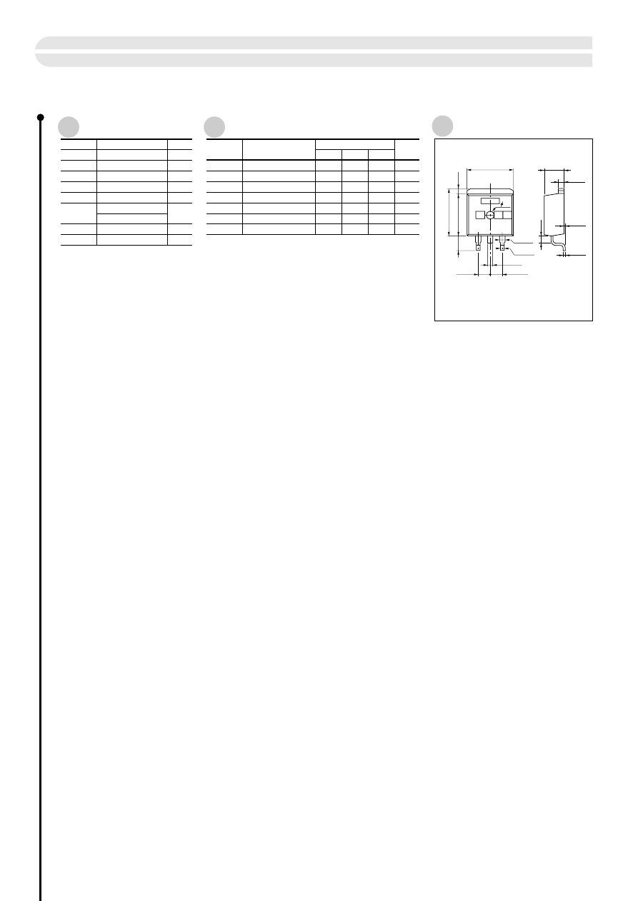
Absolute Maximum Ratings
Electrical Characteristics
Symbol
Ratings
Unit
(Ta=25ºC)
(Ta=25ºC)
V
CBO
115
±
10
Symbol
Test Conditions
Ratings
Unit
I
CBO
µ
A
V
CB
=105V
min
I
EBO
µ
A
V
EB
=6V
V
CEO
V
I
C
=50mA
h
FE
V
CE
=1V, I
C
=1A
105
V
CE
(sat)
V
I
C
=1.2A, I
B
=12mA
400
V
CEO
V
V
115
±
10
V
EBO
V
6
I
C
A
I
B
A
1
P
C
W
50 (Tc=25ºC)
1.2 (Ta=25ºC, No Fin)
Tj
ºC
150
Tstg
ºC
–55 to +150
V
FEC
V
I
FEC
=6A
E
S/B
mJ
L=10mA
45
typ
115
0.08
800
1.25
10
max
10
125
0.12
1500
1.5
±
6 (pulse
±
10)
Power Transistor MN611S
79
External Dimensions
TO220S
a
b
10.2
±
0.3
1.27
±
0.2
2.54
±
0.5
2.54
±
0.5
1.2
±
0.2
1.6
10.0
8.6
±
0.3
(1.4)
–
0.5
+0.3
–
0.5
+0.3
3.0
0.86
–0.1
+0.2
–0.1
+0.2
4.44
±
0.2
1.3
±
0.2
0.4
±
0.1
(1.5)
0.1
a) Part No.
b) Lot No.
(Unit: mm)
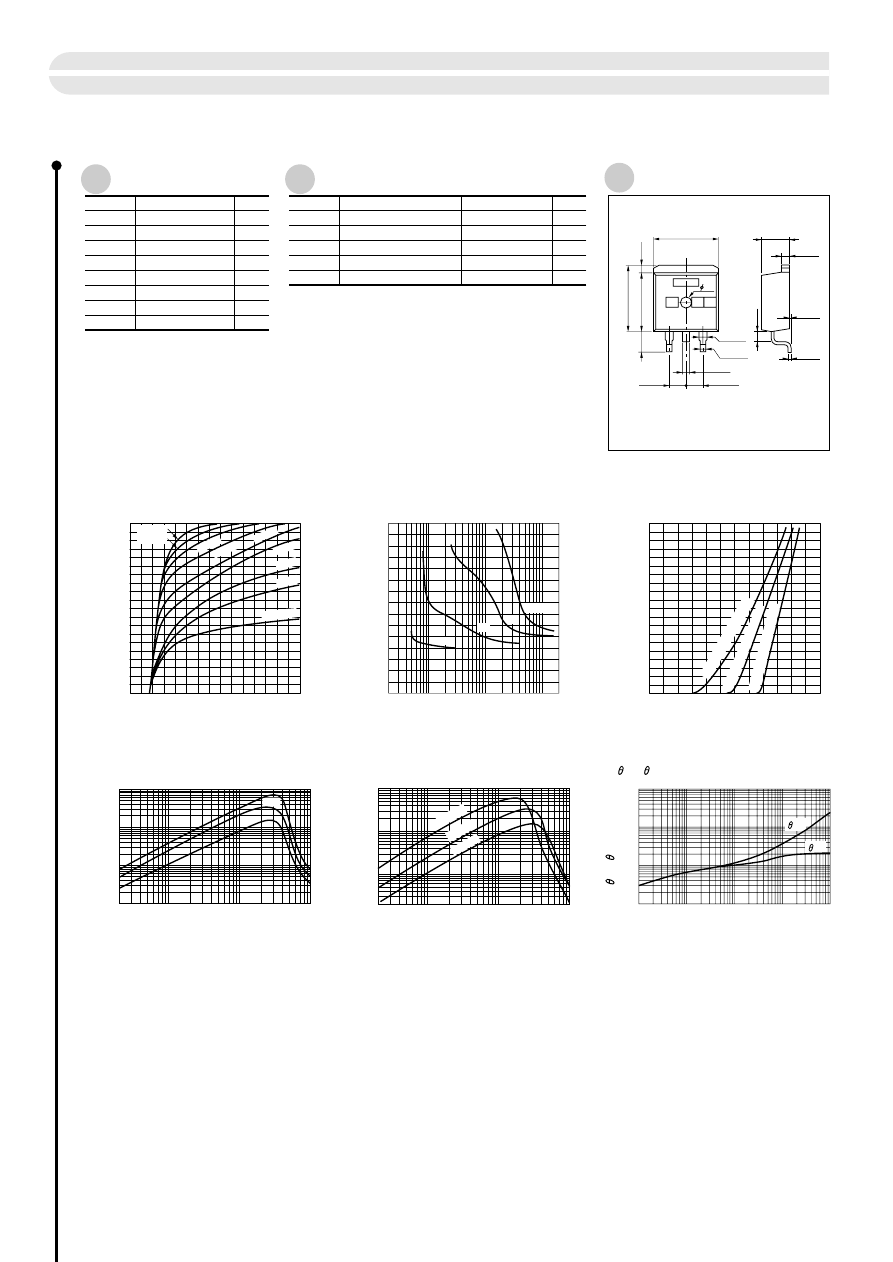
Absolute Maximum Ratings
Electrical Characteristics
Symbol
Ratings
Unit
(Ta=25ºC)
(Ta=25ºC)
V
CBO
380
±
50
Symbol
Test Conditions
Ratings
Unit
I
CBO
µ
A
V
CB
=330V
10max
I
EBO
mA
V
EB
=6V
20max
V
(BR) CEO
V
I
C
=25mA
h
FE
V
CE
=2V, I
C
=3A
330 to 430
V
CE
(sat)
V
I
C
=4A, I
B
=20mA
1.5max
1500min
V
CEO
V
V
380
±
50
V
EBO
V
6
I
C
A
I
B
A
1
P
C
W
60 (Tc=25ºC)
Tj
ºC
150
Tstg
ºC
–55 to +150
6 (pulse 10)
■
I
C
— V
CE
Characteristics (typ.)
■
I
C
— V
BE
Temperature Characteristics (typ.)
■
h
FE
— I
C
Characteristics (typ.)
■
h
FE
— I
C
Temperature Characteristics (typ.)
■
j-c
•
j-a
—t
Characteristics
■
V
CE
(sat) — I
B
Characteristics (typ.)
Power Transistor MN638S
80
0
0
5
10
2
4
6
I
B=
1mA
2mA
4mA
18mA
20mA
90mA
60mA
0
3
2
1
0.2
1
0.5
10
5
200
100
50
1A
3A
5A
I
C
= 7A
0.02
0.1
1
0.5
10
5
5000
10000
1000
500
100
10
50
Typ
0.1
1
10
100
0.1
1
0.01
0.001
10
0
10
5
0
2.0
2.4
1.0
0.02
0.1
1.0
5
0.5
10
5000
10000
1000
500
100
50
20
125
ºC
–55
ºC
25
ºC
V
CE
(V)
I
C
(A)
120mA
150mA
I
B
(mA)
V
CE
(sat)
(V)
V
BE
(V)
I
C
(A)
(V
BE
=4V)
25
ºC (C
ase tem
perature)
125
ºC (Case temperature)
–
3
0
º
C
(C
a
s
e
te
m
p
e
ra
tu
re
)
t (s)
(V
CE
= 2V)
(V
CE
= 2V)
I
C
(A)
I
C
(A)
h
FE
h
FE
External Dimensions
TO220S
j-a
j-c
a
b
10.2
±
0.3
1.27
±
0.2
2.54
±
0.5
2.54
±
0.5
1.2
±
0.2
1.6
10.0
8.6
±
0.3
(1.4)
3.0
–
0.5
+0.3
–
0.5
+0.3
0.86
–0.1
+0.2
–0.1
+0.2
4.44
±
0.2
1.3
±
0.2
0.4
±
0.1
(1.5)
0.1
a) Part No.
b) Lot No.
(Unit: mm)
j-
c
•
j-
a
(º
C/
W)
0
2
1
3
0
0.5
1
5
■
V
CE
(sat)
— I
C
Temperature Characteristics
V
CE
(sat)
(V)
I
C
(A)
1
10
100
400
■
V
CE
(sat)
— I
B
Temperature Characteristics
0
0.25
0.5
V
CE
(sat)
(V)
I
B
(mA)
I
C
/I
B
= 100
(I
C
= 0.5A)
Ta = 125ºC
75ºC
25ºC
–40ºC
Ta = 125ºC
75ºC
25ºC
–40ºC
0
50
150
100
0
10
P
T
(W)
Ta (ºC)
20
Without heatsink
With infinite heatsink
Symbol
Ratings
Unit
(Ta=25ºC)
(Ta=25ºC)
V
CBO
35
±
5
Symbol
Test Conditions
Ratings
Unit
I
CBO
µ
A
V
CB
= 30V
10max
I
EBO
mA
V
EB
= 6V
2.7max
V
CEO
V
I
C
= 25mA
31 to 41
h
FE
V
CE
= 4V, I
C
= 0.7A
400min
V
CE
(sat)
V
V
I
C
= 0.5A, I
B
= 5mA
I
C
= 1A, I
B
= 5mA
0.2max
0.5max
V
FEC
R
B
R
BE
V
Ω
k
Ω
I
FEC
= 2A
2.5max
800
±
120
2.0
±
0.4
Es/b
mJ
L = 10mH, single pulse
50min
V
CEO
V
V
36
±
5
V
EBO
V
6
I
C
A
2 (pulse 3*)
3 (Ta=25ºC)
13.5 (Tc=25ºC)
I
B
mA
30
P
T
W
W
Tj
ºC
150
Tstg
ºC
–55 to +150
* P
W
1ms, Duty 25%
12
V
CC
(V)
12
R
L
(
Ω
)
1
I
C
(A)
10
V
BB1
(V)
–5
V
BB2
(V)
5
I
B1
(mA)
0
I
B2
(mA)
1.0
t
on
(
µ
s)
8.5
t
stg
(
µ
s)
2.5
t
f
(
µ
s)
Absolute Maximum Ratings
Electrical Characteristics
Typical Switching Characteristics
R
B
3
2
4
5
6
7
8
1
R
BE
0
1
4
5
2
6
3
■
I
C
— V
CE
Characteristics (typ.)
0
2
I
C
(A)
V
CE
(V)
1
3
0.01
0.1
4
0.5
1
■
h
FE
— I
C
Temperature Characteristics
50
100
h
FE
I
C
(A)
3000
1000
500
0
0.5
1.0
1.5
2.0
■
t
on•
t
stg •
t
f
— I
C
Characteristics (typ.)
0.1
0.5
5
1
10
t
on
•
t
stg
•
t
f
(
µ
S)
Ic (A)
50
1
5
10
50
■
Safe Operating Area (single pulse)
0.5
0.1
1
5
I
C
(A)
V
CE
(V)
(per element)
I
B
= 1mA
2mA
3mA
V
CC
= 12V
I
B
= 5mA
–I
B
= 0A
(V
CE
= 4V)
■
P
T
— Ta Derating
10ms
1ms
1
10
100
1000
■
j-a
— t Characteristics
1
5
10
j-a
(
ºC/
W)
t (ms)
20
Single pulse
30mA
12m
A
8mA
5mA
Ta = 125ºC
75ºC
25ºC
–40ºC
t
stg
t
on
Without heatsink
natural air cooling
Power Transistor Array STA315A
81
t
f
a) Part No.
b) Lot No.
(Unit: mm)
a
b
7 •2.54=17.78
±
0.25
(2.54)
20.2
±
0.2
0.5
±
0.15
1.0
±
0.25
C1.5
±
0.5
4.0
±
0.2
1.
2
±
0.2
0.5
±
0.15
1
3
2
4
E
B
C
B
5
6
7
8
C
B
C
E
9.0
±
0.2
2.3
±
0.2
11.3
±
0.2
4.7
±
0.5
External Dimensions
STA3 (LF400A)
Equivalent Circuit Diagram
Absolute Maximum Ratings
Electrical Characteristics
Typical Switching Characteristics
0
1
2
3
■
I
C
— V
CE
Characteristics (typ.)
0
2
I
C
(A)
V
CE
(V)
1
3
0
2
1
4
3
0
0.5
1.0
1.5
■
I
C
— V
BE
Temperature Characteristics (typ.)
I
C
(A)
V
BE
(V)
0.01
0.05
0.1
3
0.5
1
■
h
FE
— I
C
Temperature Characteristics (typ.)
100
h
FE
I
C
(A)
5000
1000
500
0.1
0.05
0.5
1
5
■
t
on•
t
stg•
t
f
— I
C
Characteristics (typ.)
0.3
0.5
5
1
10
t
on
•
t
stg
•
t
f
(
µ
S)
Ic (A)
20
2
5
10
50
■
Safe Operating Area (single pulse)
0.5
0.2
1
5
I
C
(A)
V
CE
(V)
10
(per element)
0.002
0.01
0.05 0.1
0.4
■
V
CE
(sat) — I
B
Temperature Characteristics
0
0.5
1
V
CE
(sat)
(V)
I
B
(A)
I
B
=1mA
2mA
3mA
V
CE
= 12V
I
B1
= –I
B2
= 5mA
V
CE
= 4V
(I
C
= 1A)
(V
CE
= 4V)
0
50
150
100
■
P
T
— Ta Derating
0
10
5
P
T
(W)
Ta (ºC)
15
Ta = –55ºC
25ºC
75ºC
125ºC
10ms
1ms
100m
Ta = 125ºC
75ºC
25ºC
–55ºC
0.1
1
10
100
1000
5000
■
j-a
— t Characteristics
0.1
0.5
1
5
10
j-a
(
ºC/
W)
t (ms)
20
Single pulse
15mA 10m
A
8mA
6mA
5mA
4mA
Ta = 125ºC
75ºC
25ºC
–55ºC
t
stg
t
f
t
on
Without heatsink (All circuits operate)
With infinite heatsink (All circuits operate)
DC (Tc
=2
5ºC)
Symbol
Ratings
Unit
(Ta=25ºC)
(Ta=25ºC)
V
CBO
35
±
5
Symbol
Test Conditions
Ratings
Unit
I
CBO
µ
A
V
CB
= 30V
10max
I
EBO
µ
A
V
EB
= 6V
10max
V
CEO
V
I
C
= 25mA
35
±
5
h
FE
V
CE
= 4V, I
C
= 0.5A
500min
V
CE
(sat)
V
I
C
= 1A, I
B
= 5mA
0.5max
Es/b
mJ
L = 10mH, single pulse
150min
V
CEO
V
V
35
±
5
V
EBO
V
6
I
C
A
3
2.5 (Ta=25ºC)
12 (Tc=25ºC)
I
B
A
1
P
T
W
W
Tj
ºC
150
Tstg
ºC
–55 to +150
12
V
CC
(V)
12
R
L
(
Ω
)
1
I
C
(A)
10
V
BB1
(V)
–5
V
BB2
(V)
5
I
B1
(mA)
5
I
B2
(mA)
1.3
t
on
(
µ
s)
4.7
t
stg
(
µ
s)
1.2
t
f
(
µ
s)
2
4
3
7
5
6
Power Transistor Array STA335A
82
Equivalent Circuit Diagram
a) Part No.
b) Lot No.
(Unit: mm)
a
b
7•2.54=17.78
±
0.25
(2.54)
20.2
±
0.2
0.5
±
0.15
1.0
±
0.25
C1.5
±
0.5
4.0
±
0.2
1.
2
±
0.2
0.5
±
0.15
1
3
2
4
C
B
E
5
6
7
8
E
B
C
9.0
±
0.2
2.3
±
0.2
11.3
±
0.2
4.7
±
0.5
External Dimensions
STA3 (LF400A)
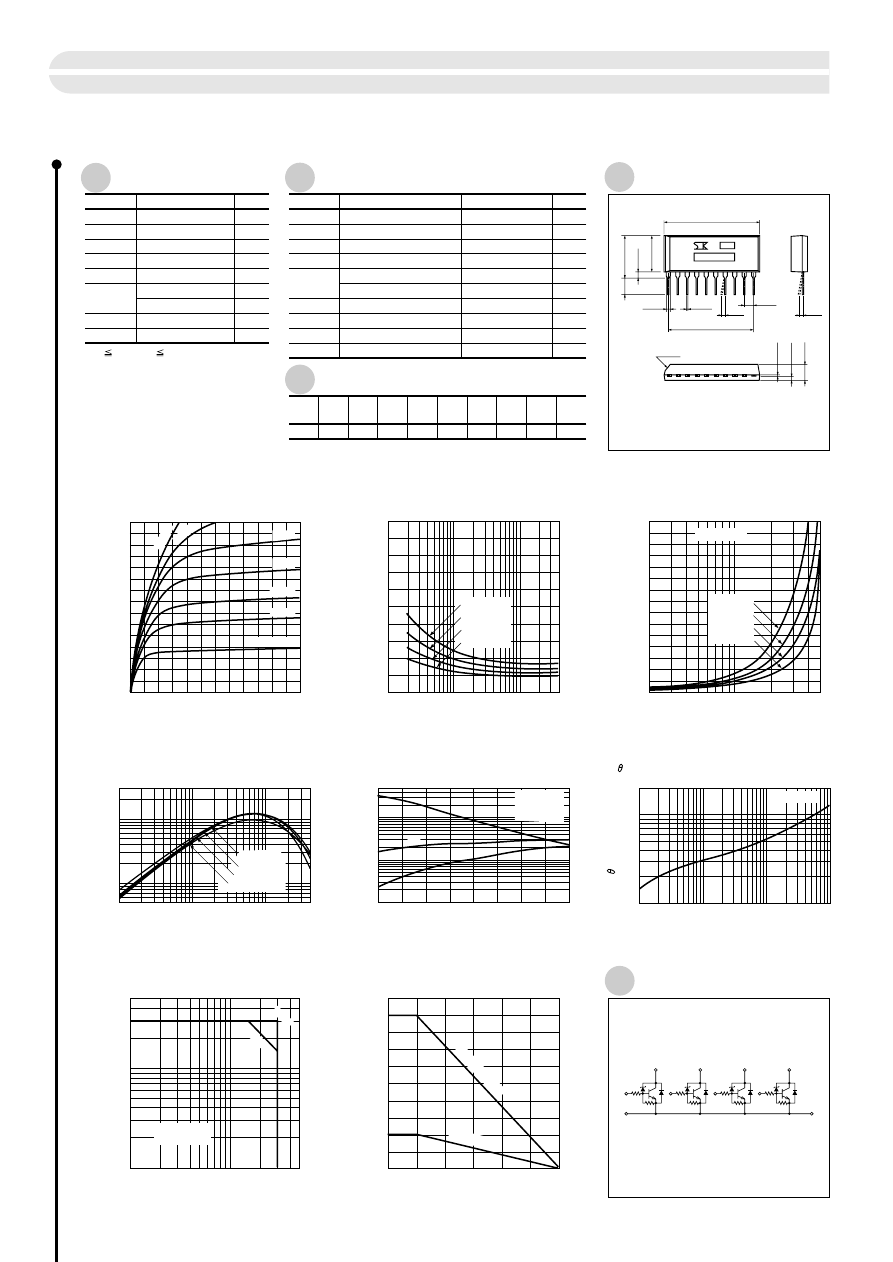
0
1
4
5
2
6
3
■
I
C
— V
CE
Characteristics (typ.)
0
2
I
C
(A)
V
CE
(V)
1
3
0.01
0.1
4
0.5
1
■
h
FE
— I
C
Temperature Characteristics
50
100
h
FE
I
C
(A)
3000
1000
500
0
0.5
1.0
1.5
2.0
■
t
on•
t
stg•
t
f
— I
C
Characteristics (typ.)
0.1
0.5
5
1
10
t
on
•
t
stg
•
t
f
(
µ
S)
Ic (A)
50
1
5
10
50
■
Safe Operating Area (single pulse)
0.5
0.1
1
5
I
C
(A)
V
CE
(V)
(per element)
I
B
= 1mA
2mA
3mA
V
CC
= 12V
I
B
= 5mA
–I
B
= 0A
(V
CE
= 4V)
0
50
150
100
■
P
T
— Ta Derating
0
10
P
T
(W)
Ta (ºC)
20
10ms
1ms
0
2
1
3
0
0.5
1
5
■
V
CE
(sat) — I
C
Temperature Characteristics
V
CE
(sat)
(V)
I
C
(A)
1
10
100
400
■
V
CE
(sat) — I
B
Temperature Characteristics
0
0.25
0.5
V
CE
(sat)
(V)
I
B
(mA)
I
C
/I
B
= 100
(I
C
= 0.5A)
Ta = 125ºC
75ºC
25ºC
–40ºC
Ta = 125ºC
75ºC
25ºC
–40ºC
1
10
100
1000
■
j-a
— t Characteristics
1
5
10
j-a
(
ºC/
W)
t (ms)
20
Single pulse
30mA
12m
A
8mA
5mA
Ta = 125ºC
75ºC
25ºC
–40ºC
t
stg
t
on
Without heatsink
With infinite heatsink
Without heatsink
natural air cooling
R
B
3
2
4
5
6
7
8
9
10
1
R
BE
Power Transistor Array STA415A
83
Symbol
Ratings
Unit
(Ta=25ºC)
(Ta=25ºC)
V
CBO
35
±
5
Symbol
Test Conditions
Ratings
Unit
I
CBO
µ
A
V
CB
= 30V
10max
I
EBO
mA
V
EB
= 6V
2.7max
V
CEO
V
I
C
= 25mA
31 to 41
h
FE
V
CE
= 4V, I
C
= 0.7A
400min
V
CE
(sat)
V
V
I
C
= 0.5A, I
B
= 5mA
I
C
= 1A, I
B
= 5mA
0.2max
0.5max
V
FEC
R
B
R
BE
V
Ω
k
Ω
I
FEC
= 2A
2.5max
800
±
120
2.0
±
0.4
Es/b
mJ
L = 10mH, single pulse
50min
V
CEO
V
V
36
±
5
V
EBO
V
6
I
C
A
2 (pulse 3*)
4 (Ta = 25ºC)
18 (Tc = 25ºC)
I
B
mA
30
P
T
W
W
Tj
ºC
150
Tstg
ºC
–55 to +150
* P
W
1ms, Duty 25%
12
V
CC
(V)
12
R
L
(
Ω
)
1
I
C
(A)
10
V
BB1
(V)
–5
V
BB2
(V)
5
I
B1
(mA)
0
I
B2
(mA)
1.0
t
on
(
µ
s)
8.5
t
stg
(
µ
s)
2.5
t
f
(
µ
s)
Absolute Maximum Ratings
Electrical Characteristics
Typical Switching Characteristics
t
f
Equivalent Circuit Diagram
a) Part No.
b) Lot No.
(Unit: mm)
9 • 2.54=22.86
±
0.05
a
b
(2.54)
25.25
±
0.2
9.0
±
0.2
2.3
±
0.2
11.3
±
0.2
3.
5
±
0.5
0.5
±
0.15
0
±
0.3
1.0
±
0.25
C1.5
±
0.5
4.0
±
0.2
±
0.5
±
0.15
1.2
±
0.2
1
3
2
4
E
B C B
5
6
7
10
C
B C
E
8
9
B C
0
±
0.3
External Dimensions
STA4 (LF412)
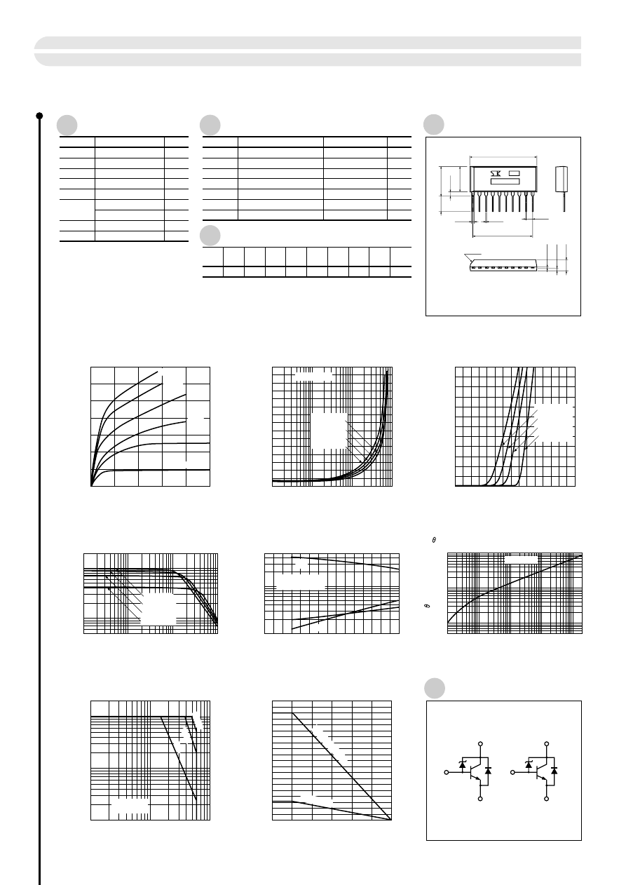
0
1
2
5
3
4
■
I
C
— V
CE
Characteristics (typ.)
0
5
4
3
2
I
C
(A)
V
CE
(V)
1
7
6
0
0.25
0.75
0.5
0.01
0.1
1
10
■
V
CE
(sat) — I
C
Temperature Characteristics (typ.)
V
CE
(sat)
(V)
I
C
(A)
0.01
0.1
10
1
■
h
FE
— I
C
Temperature Characteristics (typ.)
50
h
FE
I
C
(A)
2000
1000
500
100
0
1
2
3
■
t
on•
t
stg •
t
f
— I
C
Characteristics
0.1
0.5
1
t
on
•
t
stg
•
t
f
(
µ
S)
Ic (A)
5
1
5
10
50
100
■
Safe Operating Area (single pulse)
0.5
0.1
1
5
I
C
(A)
V
CE
(V)
20
10
0
0.5
1.0
1.5
■
I
C
— V
BE
Temperature Characteristics (typ.)
0
6
5
4
3
2
1
I
C
(A)
V
BE
(V)
I
B
= 1mA
3mA
V
CC
= 12V
I
B1
= –I
B2
= 30mA
I
C
/ I
B
= 100
(V
CE
= 1V)
(V
CE
= 1V)
0
50
150
100
0
10
15
5
P
T
(W)
Ta (ºC)
20
Ta = –55ºC
25ºC
75ºC
125ºC
1ms
0.5ms
10m
s
Ta = 125ºC
75ºC
25ºC
–55ºC
0.1
1
10
100
2000
■
j-a
— t Characteristics
0.05
0.1
0.5
1
5
j-a
(º
C/
W)
t (ms)
10
Single pulse
10mA
30mA
20mA
5mA
Ta = 125ºC
75ºC
25ºC
–55ºC
t
f
t
on
Without heatsink
With infinite heatsink
t
stg
Without heatsink
natural air cooling
Symbol
Ratings
Unit
(Ta=25ºC)
(Ta=25ºC)
V
CBO
65
±
5
Symbol
Test Conditions
Ratings
Unit
I
CBO
µ
A
V
CB
= 60V
10max
I
EBO
µ
A
V
EB
= 6V
10max
V
CEO
V
I
C
= 50mA
60 to 70
h
FE
V
CE
= 1V, I
C
= 1A
400 to 1500
V
CE
(sat)
V
I
C
= 1.5A, I
B
= 15mA
0.15max
V
FEC
V
I
FEC
= 6A
1.5max
Es/b
mJ
L = 10mH, single pulse
80min
V
CEO
V
V
65
±
5
V
EBO
V
6
I
C
A
±
6 (pulse
±
10)
3.2 (Ta = 25ºC)
18 (Tc = 25ºC)
I
B
A
1
P
T
W
W
Tj
ºC
150
Tstg
ºC
–55 to +150
12
V
CC
(V)
12
R
L
(
Ω
)
1
I
C
(A)
10
V
BB1
(V)
–5
V
BB2
(V)
30
I
B1
(mA)
–30
I
B2
(mA)
0.2
t
on
(
µ
s)
3.9
t
stg
(
µ
s)
0.2
t
f
(
µ
s)
Absolute Maximum Ratings
Electrical Characteristics
Typical Switching Characteristics
3
2
4
8
7
9
■
P
T
— Ta Derating
Power Transistor Array STA461C
84
Equivalent Circuit Diagram
a) Part No.
b) Lot No.
(Unit: mm)
9 • 2.54=22.86
±
0.05
a
b
(2.54)
25.25
±
0.2
9.0
±
0.2
2.3
±
0.2
11.3
±
0.2
4.7
±
0.5
0.5
±
0.15
1.0
±
0.25
C1.5
±
0.5
±
4.0
±
0.2
0.5
±
0.15
1.2
±
0.2
1
3
2
4
B C E
5
6
7
10
B
8
9
C E
External Dimensions
STA4 (LF400B)
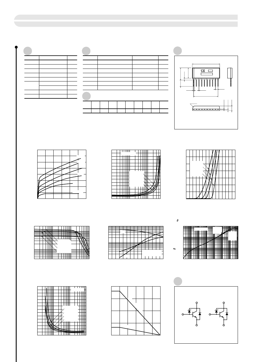
Absolute Maximum Ratings
Electrical Characteristics
Typical Switching Characteristics
0
1
2
6
5
3
4
0
5
4
3
2
I
C
(A)
V
CE
(V)
1
8
7
6
0
0.25
0.75
0.5
0.01
0.1
1
5
V
CE
(sat)
(V)
I
C
(A)
0.01
0.1
10
1
30
50
h
FE
I
C
(A)
2000
1000
500
100
0
1
2
3
0.1
0.5
1
t
on
•
t
stg
•
t
f
(
µ
S)
Ic
(A)
10
5
(Tc = 25ºC)
0
0.5
1.0
1.5
0
7
6
5
4
3
2
1
I
C
(A)
V
BE
(V)
I
B
= 1mA
3mA
V
CC
= 12V
I
B1
= –I
B2
= 30mA
I
C
/I
B
= 100
(V
CE
= 1V)
(V
CE
= 4V)
0
50
150
100
0
10
5
P
T
(W)
Ta
(ºC)
20
15
Ta = –55ºC
25ºC
75ºC
150ºC
0
0.25
0.75
0.5
1
10
100
1000
V
CE
(sat)
(V)
I
B
(mA)
I
C
= 1.2A
Ta = 150ºC
75ºC
25ºC
–55ºC
Ta = 150ºC
75ºC
25ºC
–55ºC
0.0001
1
0.1
0.01
0.001
10
100
1000
0.1
0.5
1
5
10
50
j-a
(º
C/
W)
t
(s)
100
Single pulse
10mA
30mA
20mA
5mA
Ta = 150ºC
75ºC
25ºC
–55ºC
t
f
t
on
Without heatsink
With infinite heatsink
t
stg
Dual
transistor
operated
Single
transistor
operated
Symbol
Ratings
Unit
(Ta=25ºC)
(Ta=25ºC)
V
CBO
115
±
10
Symbol
Test Conditions
Ratings
Unit
I
CBO
µ
A
V
CB
= 105V
10max
I
EBO
µ
A
V
EB
= 6V
10max
V
CEO
V
I
C
= 50mA
105 to 125
h
FE
V
CE
= 1V, I
C
= 1A
400 to 1500
V
CE
(sat)
V
I
C
= 1.2A, I
B
= 12mA
0.12max
V
FEC
V
I
FEC
= 6A
1.5max
Es/b
mJ
L = 10mH, single pulse
45min
V
CEO
V
V
115
±
10
V
EBO
V
6
I
C
A
±
6 (pulse
±
10)
3.2 (Ta=250ºC)
18 (Tc=25ºC)
I
B
A
1
P
T
W
W
Tj
ºC
150
Tstg
ºC
–55 to +150
12
V
CC
(V)
12
R
L
(
Ω
)
1
I
C
(A)
10
V
BB1
(V)
–5
V
BB2
(V)
30
I
B1
(mA)
–30
I
B2
(mA)
0.2
t
on
(
µ
s)
5.7
t
stg
(
µ
s)
0.4
t
f
(
µ
s)
3
2
4
8
7
9
■
I
C
— V
CE
Characteristics (typ.)
■
V
CE
(sat) — I
C
Temperature Characteristics (typ.)
■
V
CE
(sat)
— I
B
Temperature Characteristics (typ.)
■
h
FE
— I
C
Temperature Characteristics (typ.)
■
t
on•
t
stg •
t
f
— I
C
Characteristics
■
I
C
— V
BE
Temperature Characteristics (typ.)
■
j-a
— t Characteristics
■
P
T
— Ta Derating
Power Transistor Array STA463C
85
Equivalent Circuit Diagram
a) Part No.
b) Lot No.
(Unit: mm)
9 •2.54=22.86
±
0.05
a
b
(2.54)
25.25
±
0.2
9.0
±
0.2
2.3
±
0.2
11.3
±
0.2
4.7
±
0.5
0.5
±
0.15
1.0
±
0.25
C1.5
±
0.5
4.0
±
0.2
0.5
±
0.15
1.2
±
0.2
1
3
2
4
B C E
5
6
7
10
B
8
9
C E
External Dimensions
STA4 (LF400B)
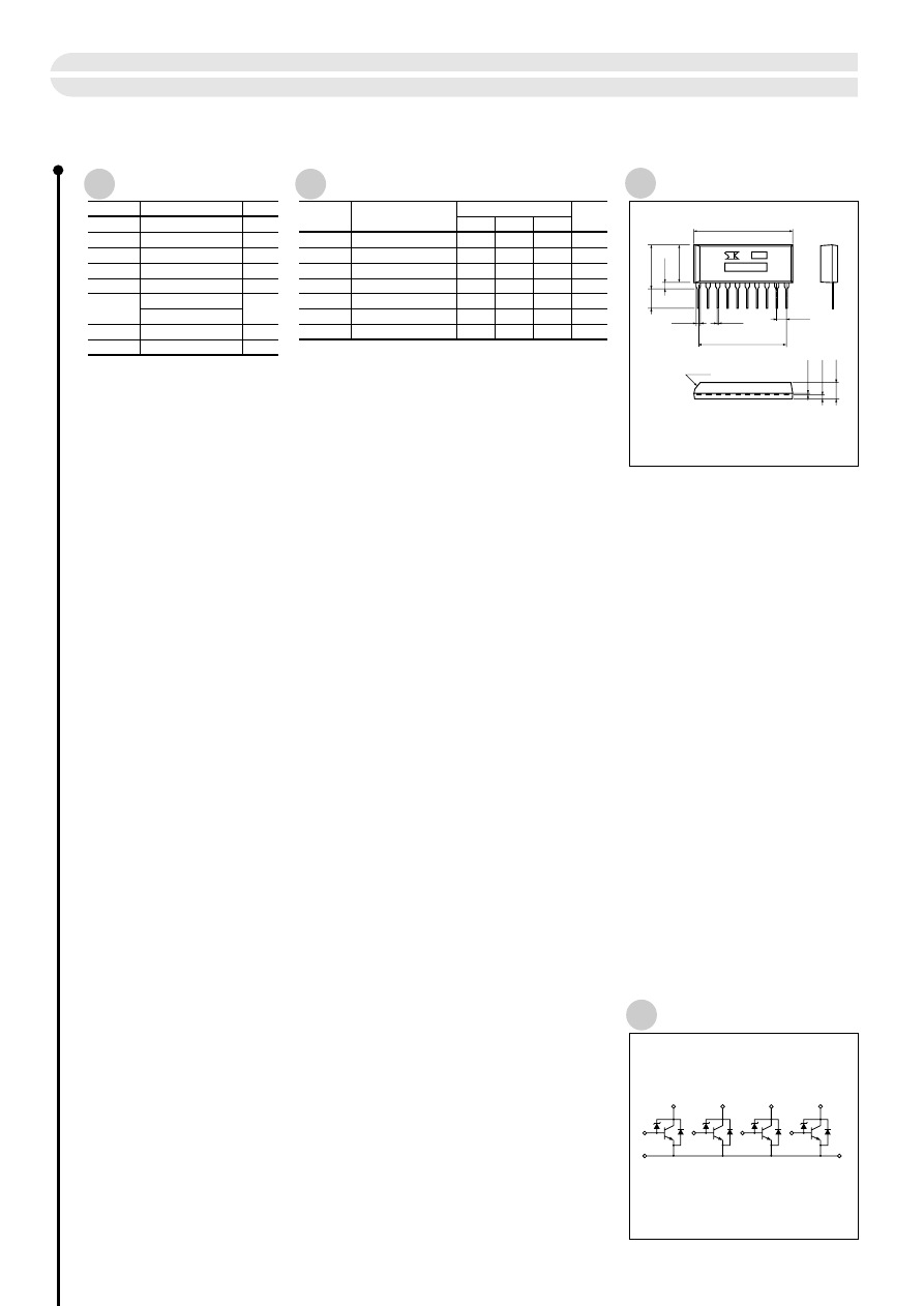
Absolute Maximum Ratings
Electrical Characteristics
Symbol
Ratings
Unit
(Ta=25ºC)
(Ta=25ºC)
V
CBO
65
±
5
Symbol
Test Conditions
Ratings
Unit
I
CBO
µ
A
V
CB
=60V
I
EBO
µ
A
V
EB
=6V
V
CEO
V
I
C
=50mA
60
h
FE
V
CE
=1V, I
C
=1A
400
V
CE
(sat)
V
I
C
=1.5A, I
B
=15mA
V
FEC
V
I
FEC
=6A
Es/b
mJ
L=10mH
80
65
800
0.09
1.25
10
max
typ
min
10
70
1500
0.15
1.5
V
CEO
V
V
65
±
5
V
EBO
V
6
I
C
A
6 (pulse 10)
20 (Tc=25ºC)
4 (Ta=25ºC)
I
B
A
1
P
C
W
Tj
ºC
150
Tstg
ºC
–55 to +150
3
2
1
5
4
7
6
9
8
10
Power Transistor Array STA464C
86
Equivalent Circuit Diagram
a) Part No.
b) Lot No.
(Unit: mm)
9 •2.54= (22.86)
±
0.05
a
b
(2.54)
25.25
±
0.2
9.0
±
0.2
2.3
±
0.2
11.3
±
0.2
3.5
±
0.5
0.5
±
0.15
1.0
±
0.25
C1.5
±
0.5
4.0
±
0.2
0.5
±
0.15
1.2
±
0.2
1
3
2
4
B
B
C
B
C
C
E
5
6
7
10
B
8
9
C E
External Dimensions
STA4
(Root dimension)
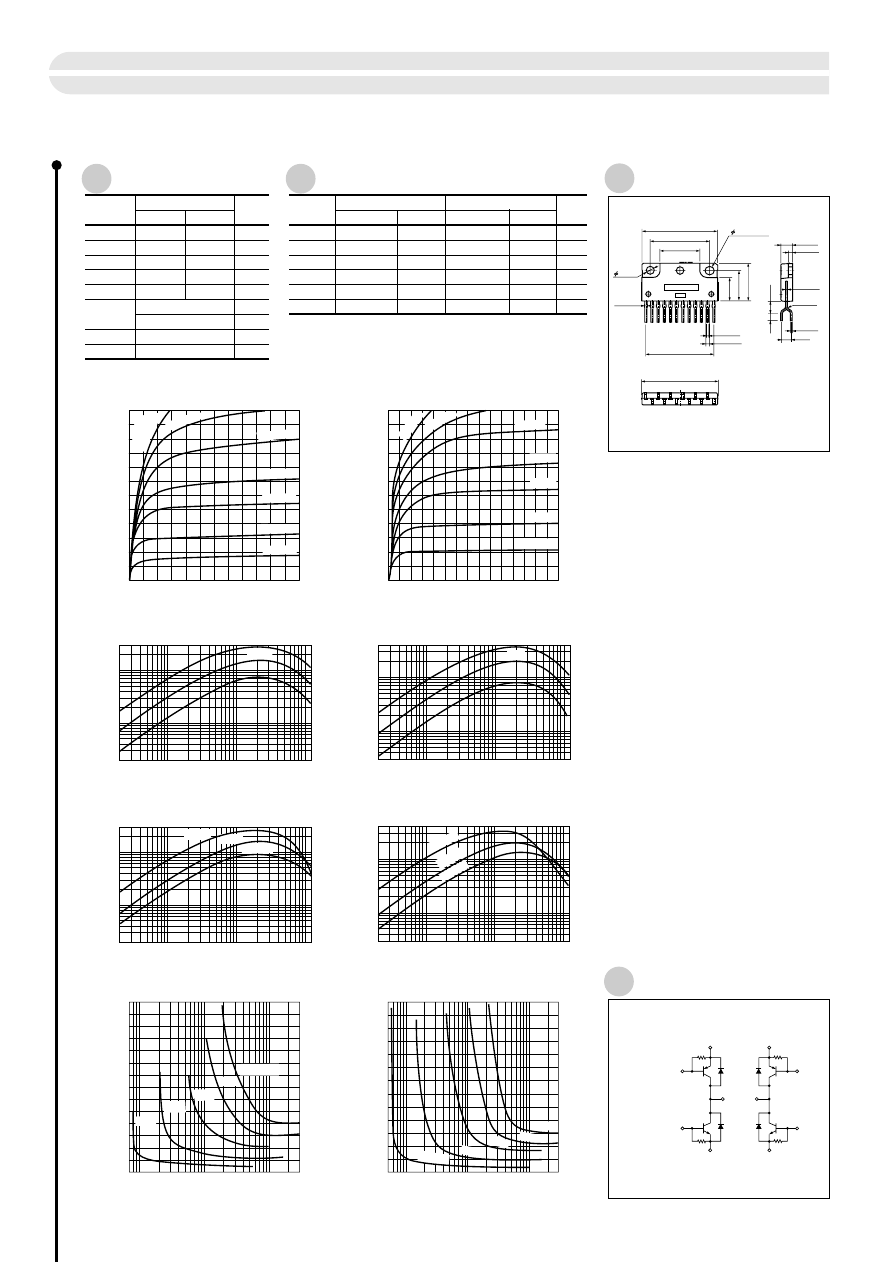
Absolute Maximum Ratings
Electrical Characteristics
Symbol
Ratings
NPN
PNP
Unit
(Ta=25ºC)
(Ta=25ºC)
V
CBO
60
–55
–55
–6
–12
–3
Symbol
Test Conditions
NPN
PNP
Ratings
Test Conditions
Ratings
Unit
I
CBO
µ
A
V
CB
= 60V
100max
I
EBO
mA
V
EB
= 6V
60max
V
CEO
V
I
C
= 25mA
60min
h
FE
V
CE
= 1V, I
C
= 3A
150min
V
CE
(sat)
V
I
C
= 6A, I
B
= 0.3A
0.35max
V
FEC
V
I
FEC
= 10A
2.5max
V
CB
= –55V
–100max
V
EB
= –6V
–60max
I
C
= –25mA
–55min
V
CE
= –1V, I
C
= –3A
80min
I
C
= –6A, I
B
= –0.3A
–0.35max
I
FEC
= 10A
2.5max
V
CEO
V
V
60
V
EBO
V
6
12
I
C
A
I
B
A
3
P
T
W
W
5 (Tc=25ºC, No Fin)
40 (Tc=25ºC)
Tj
150
Tstg
ºC
ºC
–55 to +150
8
4
9
7
10
3
6
12
11
1
2
R
1
: 500
Ω
Typ.
R
2
: 500
Ω
Typ.
R
1
R
2
5
Power Transistor Array SLA8004
87
Equivalent Circuit Diagram
a) Part No.
b) Lot No.
(Unit: mm)
3.2
±
0.15
•3.8
11• P2.54
±
0.1
= (27.94)
3.2
±
0.15
31
±
0.2
4.8
±
0.2
1.7
±
0.1
2.45
±
0.2
4 – (R1)
R-end
4
±
0.7
24.4
±
0.2
9.9
±
0.2
12.9
±
0.2
16
±
0.2
5
±
0.5
(3)
1.2
±
0.15
0.85
1.45
±
0.15
31.3
±
0.2
16.4
±
0.2
(Root dimension)
(Root dimension)
+0.2
–0.1
0.55
1 2 3 4 5 6 7 8 9 10
12
11
a
b
External Dimensions
SLA (LF817)
+0.2
–0.1
■
I
C
— V
CE
Characteristics (typ.)
0
0
–8
–4
–12
–6
–2
–10
–2
–1
–3
–4
–5
–6
–40mA
–60mA
–100mA
–150mA
–20mA
–10mA
I
B
=
–
200mA
V
CE
(V)
I
C
(A)
■
h
FE
— I
C
Characteristics (typ.)
–0.02
–0.1
–1
–12
–10
2
10
300
100
Typ
I
C
(A)
h
FE
( V
C E
= –1 V ) ( P N P )
( P N P )
■
h
FE
— I
C
Temperature Characteristics (typ.)
–0.02
–0.1
–1
–12
–10
2
10
300
100
125ºC
25ºC
–30ºC
( P N P )
( V
C E
= –1 V )
I
C
(A)
h
FE
■
V
CE
(sat) — I
B
Characteristics (typ.)
0
–1.4
–1.0
–0.5
–7
–100
–10
–1000 –3000
I
B
(mA)
V
CE
(sat)
(V)
–1A
–3A
–6A
–9A
I
C
= –12A
( P N P )
( N P N )
■
I
C
— V
CE
Characteristics (typ.)
0
0
4
2
8
6
12
10
2
4
6
200mA
I
B
= 10mA
20mA
40mA
60mA
100mA
150m
A
V
CE
(V)
I
C
(A)
■
h
FE
— I
C
Temperature Characteristics (typ.)
0.02
0.1
1
10 12
3
5
50
10
100
400
25
ºC
–30
ºC
125
ºC
( N P N )
(V
CE
= 1V)
I
C
(A)
h
FE
■
h
FE
— I
C
Characteristics (typ.)
0.02
0.1
1
10 12
3
5
50
10
100
400
Typ
( N P N )
(V
CE
= 1V)
I
C
(A)
h
FE
■
V
CE
(sat) — I
B
Characteristics (typ.)
0
1.0
1.3
0.5
5
10
100
3000
1000
I
C
= 1A
12A
3A
6A
9A
I
B
(mA)
V
CE
(sat)
(V)
( N P N )
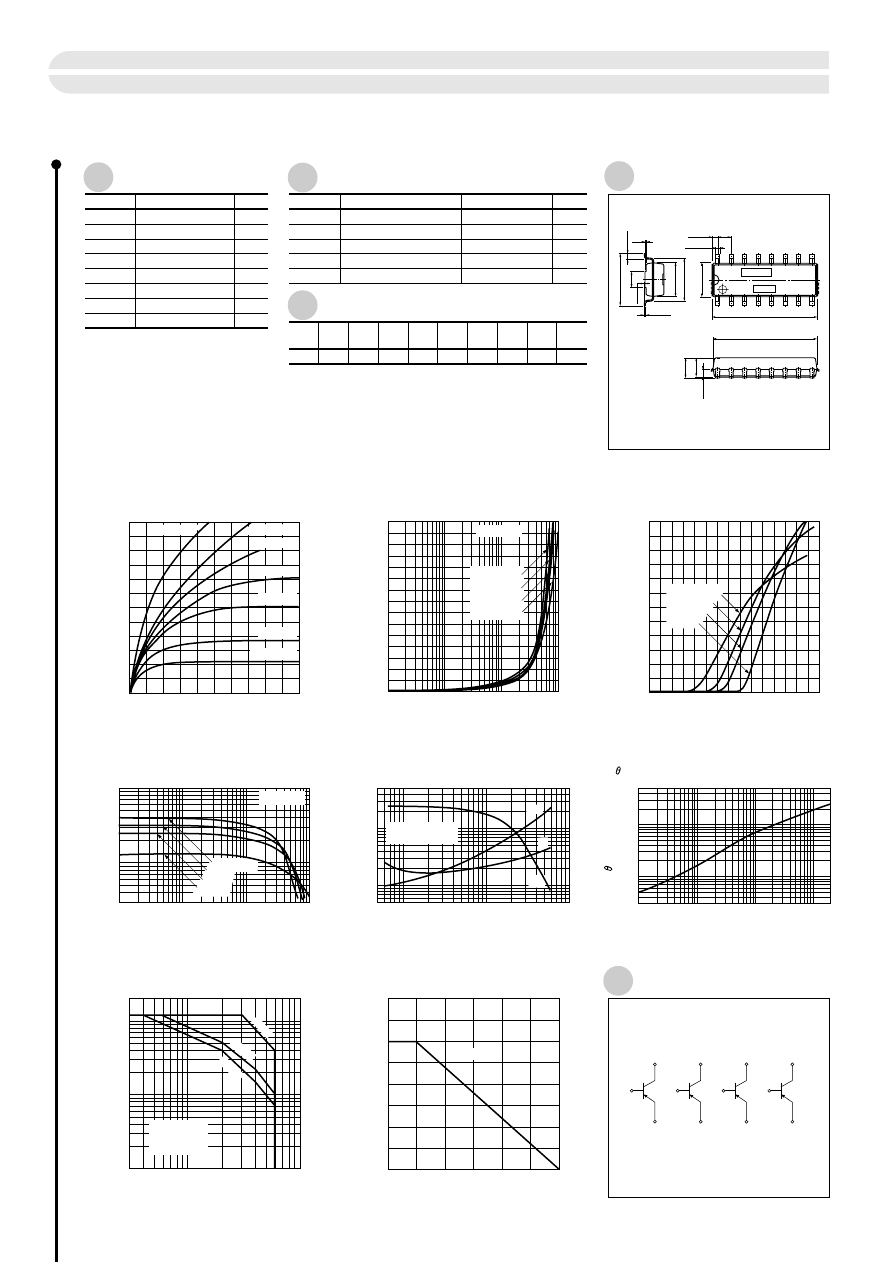
0
–1
–2
–3
–4
–5
■
I
C
— V
CE
Characteristics
0
–5
–6
I
C
(A)
V
CE
(V)
–4
–3
–2
–1
0
50
100
150
■
P
T
— Ta Derating
0
3
2
1
P
T
(W)
Ta (ºC)
4
0.001
0.01
0.1
1
2
■
j-a
— t Characteristics
0.3
1
5
10
j-a (
ºC/W)
t (s)
50
–3
–5
–10
–50
–100
■
Safe Operating Area (single pulse)
–0.1
–0.5
–10
–1
I
C
(A)
V
CE
(V)
–20
–0.05
–1
–0.1
–10
■
V
CE
(sat) — I
C
Temperature Characteristics (typ.)
0
–1
–2
V
CE
(sat)
(V)
I
C
(A)
–3
I
B
= –5mA
–10mA
–20mA
–30mA
–50mA
I
C
/I
B
= 20
Ta = 25ºC
Single pulse
0
–0.5
–1.0
–1.5
■
I
C
— V
BE
Temperature Characteristics (typ.)
0
–5
–4
–3
–2
–1
–6
I
C
(A)
V
BE
(V)
(V
CE
= –4V)
Without heatsink
20ms
10ms
1ms
–200mA
–100mA
Ta = 150ºC
75ºC
25ºC
–55ºC
Ta = 150ºC
75ºC
25ºC
–55ºC
Symbol
Ratings
Unit
(Ta=25ºC)
(Ta=25ºC)
V
CBO
–60
Symbol
Test Conditions
Ratings
Unit
I
CBO
–12
V
CC
(V)
12
R
L
(
Ω
)
–1
I
C
(A)
–10
V
BB1
(V)
5
V
BB2
(V)
–50
I
B1
(mA)
50
I
B2
(mA)
0.4
t
on
(
µ
s)
1.75
t
stg
(
µ
s)
0.22
t
f
(
µ
s)
µ
A
V
CB
= –60V
–10max
I
EBO
µ
A
V
EB
= –6V
–10max
V
CEO
V
I
C
= –25mA
–60min
h
FE
V
CE
= –4V, I
C
= –2A
100min
V
CE
(sat)
V
I
C
= –2A, I
B
= –0.1A
–0.4max
V
CEO
V
V
–60
V
EBO
V
–6
I
C
A
–6 (pulse –12)
I
B
A
–1
P
T
W
3 (No Fin)
Tj
ºC
150
Tstg
ºC
–55 to +150
Electrical Characteristics
Typical Switching Characteristics
natural air cooling
Without heatsink
15
16
2
13
14
4
11
12
6
9
10
8
Surface-mount Power Transistor Array SDA03
88
0.05
1
0.5
0.1
5
–0.5 –0.1
–0.5
–1
–5
–10
■
t
on •
t
stg •
t
f
— I
C
Characteristics
t
on
•
t
stg
•
t
f
(
µ
sec)
I
C
(A)
–0.01
–0.1
–1
–10
■
h
FE
— I
C
Temperature Characteristics
30
100
50
500
h
FE
I
C
(A)
1000
V
CE
= –4V
Ta = 150ºC
V
CC
= 12V
I
B1
= –I
B2
= 50mA
t
on
t
f
t
stg
75ºC
25ºC
–55ºC
Absolute Maximum Ratings
a) Part No.
b) Lot No.
(Unit: mm)
a
b
20.0max
2.54
±
0.25
0.89
±
0.15
8.0
±
0.5
6.3
±
0.2
0 to 0.15
3.0
±
0.2
0.25
9.8
±
0.3
1.0
±
0.3
19.56
±
0.2
6.8max
0.75
0.3
+0.15
–0.05
+0.15
–0.05
16
Pin 1
8
9
4.0max
3.6
±
0.2
1.4
±
0.2
External Dimensions
SMD-16A
Equivalent Circuit Diagram

0
50
100
150
0
3
2
1
P
T
(W)
Ta (ºC)
4
Without heatsink
Symbol
Ratings
Unit
(Ta=25ºC)
(Ta=25ºC)
V
CBO
–60
Symbol
Test Conditions
Ratings
Unit
I
CBO
–12
V
CC
(V)
12
R
L
(
Ω
)
–1
I
C
(A)
–10
V
BB1
(V)
5
V
BB2
(V)
–50
I
B1
(mA)
50
I
B2
(mA)
0.4
t
on
(
µ
s)
1.75
t
stg
(
µ
s)
0.22
t
f
(
µ
s)
µ
A
V
CB
= –60V
–10max
I
EBO
µ
A
V
EB
= –6V
–10max
V
CEO
V
I
C
= –25mA
–60min
h
FE
V
CE
= –4V, I
C
= –2A
100min
V
CE
(sat)
V
I
C
= –2A, I
B
= –0.1A
–0.4max
V
CEO
V
V
–60
V
EBO
V
–6
I
C
A
–6 (pulse –12)
I
B
A
–1
P
T
W
2.5 (No Fin)
Tj
ºC
150
Tstg
ºC
–55 to +150
Absolute Maximum Ratings
Electrical Characteristics
Typical Switching Characteristics
15
16
2
9
10
8
■
P
T
— Ta Derating
Surface-mount Power Transistor Array SDA04
89
0
–1
–2
–3
–4
–5
■
I
C
— V
CE
Characteristics
0
–5
–6
I
C
(A)
V
CE
(V)
–4
–3
–2
–1
0.05
1
0.5
0.1
5
–0.5 –0.1
–0.5
–1
–5
–10
■
t
on•
t
stg•
t
f
— I
C
Characteristics
t
on
•
t
stg
•
t
f
(
µ
sec)
I
C
(A)
–0.01
–0.1
–1
–10
■
h
FE
—
I
C
Temperature Characteristics
30
100
50
500
h
FE
I
C
(A)
1000
0.001
0.01
0.1
1
2
■
j-a
— t Characteristics
0.3
1
5
10
j-a (
ºC/
W)
t (s)
50
–3
–5
–10
–50
–100
■
Safe Operating Area (single pulse)
–0.1
–0.5
–10
–1
I
C
(A)
V
CE
(V)
–20
–0.05
–1
–0.1
–10
■
V
CE
(sat) — I
C
Temperature Characteristics (typ.)
0
–1
–2
V
CE
(sat)
(V)
I
C
(A)
–3
I
B
= –5mA
–10mA
–20mA
–30mA
–50mA
I
C
/I
B
= 20
V
CE
= –4V
Ta = 150ºC
Ta = 25ºC
Single pulse
V
CC
= 12V
I
B1
= –I
B2
= 50mA
0
–0.5
–1.0
–1.5
■
I
C
— V
BE
Temperature Characteristics (typ.)
0
–5
–4
–3
–2
–1
–6
I
C
(A)
V
BE
(V)
(V
CE
= –4V)
20ms
10ms
1ms
–200mA
–100mA
Ta = 150ºC
75ºC
25ºC
–55ºC
Ta = 150ºC
75ºC
25ºC
–55ºC
t
on
t
f
t
stg
75ºC
25ºC
–55ºC
natural air cooling
Without heatsink
Equivalent Circuit Diagram
a) Part No.
b) Lot No.
(Unit: mm)
a
b
20.0max
2.54
±
0.25
0.89
±
0.15
8.0
±
0.5
6.3
±
0.2
0 to 0.15
3.0
±
0.2
0.25
9.8
±
0.3
1.0
±
0.3
19.56
±
0.2
6.8max
0.75
0.3
+0.15
–0.05
+0.15
–0.05
16
Pin 1
8
9
4.0max
3.6
±
0.2
1.4
±
0.2
External Dimensions
SMD-16A
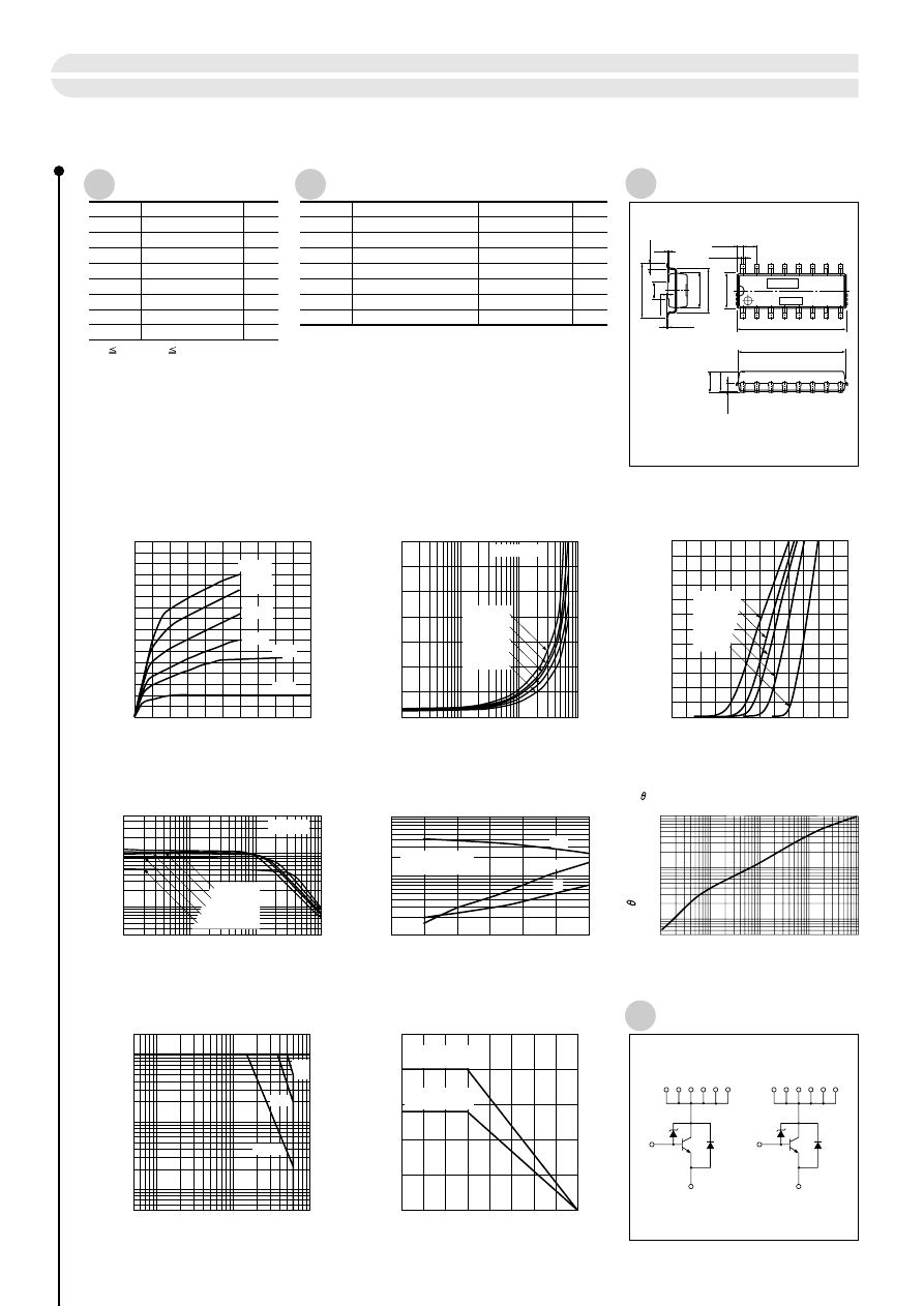
14
1
3
4
13 15 16
2
11
5
6
8
9
10 12
7
Surface-mount Power Transistor Array SDC09
90
Symbol
Ratings
Unit
(Ta=25ºC)
(Ta=25ºC)
V
CBO
65
±
5
Symbol
Test Conditions
Ratings
Unit
I
CBO
µ
A
V
CB
= 60V
10max
I
EBO
µ
A
V
EB
= 6V
10max
V
CEO
V
I
C
= 50mA
60 to 70
h
FE
V
CE
= 1V, I
C
= 1A
400 to 1500
V
CE
(sat)
V
I
C
= 1.5A, I
B
= 15mA
0.15max
V
FEC
V
I
FEC
= 6A
1.5max
Es/b
mJ
L = 10mH, single pulse
80min
V
CEO
V
V
65
±
5
V
EBO
V
6
I
C
A
6 (pulse 10 *)
I
B
A
1
P
T
W
2.8
Tj
ºC
150
Tstg
ºC
–55 to +150
* P
W
100
µ
s, Duty 1%
Absolute Maximum Ratings
Electrical Characteristics
a) Part No.
b) Lot No.
(Unit: mm)
a
b
20.0max
2.54
±
0.25
0.89
±
0.15
8.0
±
0.5
6.3
±
0.2
0 to 0.15
3.0
±
0.2
0.25
9.8
±
0.3
1.0
±
0.3
19.56
±
0.2
6.8max
0.75
0.3
+0.15
–0.05
16
Pin 1
8
9
4.0max
3.6
±
0.2
1.4
±
0.2
External Dimensions
SMD-16A
Equivalent Circuit Diagram
+0.15
–0.05
0
50
–50
100
150
0
3
2
1
P
T
(W)
Ta
(ºC)
6
5
50• 50 • 1.6mm
Use substrate
42•31•1.0mm
Use substrate
■
P
T
— Ta Derating
0
1
2
3
4
5
■
I
C
— V
CE
Characteristics
0
5
6
7
8
I
C
(A)
V
CE
(V)
4
3
2
1
1
0.1
10
0
0.5
1.0
1.5
2.0
2.5
3.0
■
t
on•
t
stg•
t
f
— I
C
Characteristics
t
on
•
t
stg
•
t
f
(
µ
sec)
I
C
(A)
0.01
0.1
1
10
■
h
FE
—
I
C
Temperature Characteristics
1000
100
50
5000
h
FE
I
C
(A)
0.1
1
10
100
1000
0.05
0.1
1
10
j-a
(º
C/W)
t
(ms)
0.5
1
5
10
50
100
■
Safe Operating Area (single pulse)
0.1
0.05
0.5
10
1
5
I
C
(A)
V
CE
(V)
20
0.0001
0.01
0.001
0.1
■
V
CE
(sat) — I
C
Temperature Characteristics (typ.)
0
0.1
0.2
0.3
0.4
0.5
0.6
0.7
V
CE
(sat)
(V)
I
C
(A)
1mA
3mA
5mA
10mA
20mA
I
C
/I
B
=100
V
CE
=1V
Ta=150ºC
Use substrate
42•31•1m
Single pulse
V
CC
=12V
I
B1
= –I
B2
=30mA
0
0.2
0.4
1.2
1.0
0.8
0.6
■
I
C
— V
BE
Temperature Characteristics (typ.)
0
5
4
3
2
1
6
I
C
(A)
V
BE
(V)
(V
CE
= 4V)
I
B
=
30mA
Ta=150ºC
100ºC
75ºC
25ºC
–55ºC
Ta=150ºC
100ºC
75ºC
25ºC
–55ºC
t
on
t
f
t
stg
75ºC
100ºC
25ºC
–55ºC
1ms
10ms
0.5
ms
Ta=25ºC
■
j-a
— t Characteristics
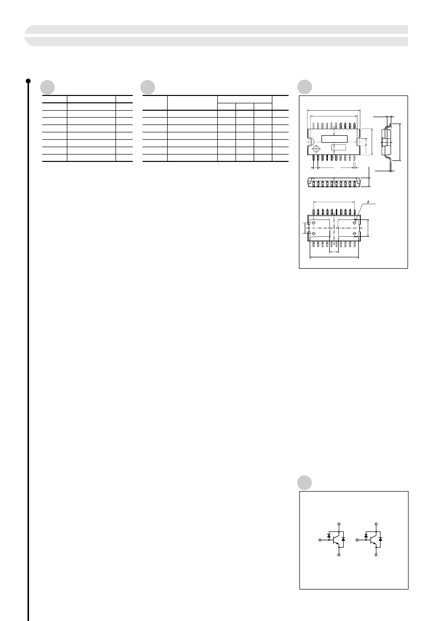
1.0
10.5
±
0.3
+0.1
–0.05
0.25
+0.15
–0.05
2.5
±
0.2
14.74
±
0.2
7.5
±
0.2
2
±
0.2
13.04
±
0.2
1.27
±
0.25
20
1
10
11
0.4
+0.15
–0.05
a
b
F1
3
18,19
F2
8
12,13
Surface-mount Power Transistor Array SPF0001
91
(Ta=25ºC)
(Ta=25ºC)
Absolute Maximum Ratings
Electrical Characteristics
External Dimensions
SMD-16A
Equivalent Circuit Diagram
Symbol
Ratings
Unit
V
CBO
115
±
10
Symbol
Test Conditions
Ratings
Unit
I
CBO
µ
A
V
CB
=105V
I
EBO
µ
A
V
EB
=6V
V
CEO
V
I
C
=50mA
105
h
FE
V
CE
=1V, I
C
=1A
400
V
CE
(sat)
V
I
C
=1.2A, I
B
=12mA
V
FEC
V
I
FEC
=6A
Es/b
mJ
L=10mH
45
115
800
0.08
1.25
10
max
typ
min
10
125
1500
0.12
1.5
V
CEO
V
V
115
±
10
V
EBO
V
6
I
C
A
±
6 (pulse
±
10)
2.5 (Ta=25ºC)
I
B
A
1
P
T
W
Tj
ºC
150
Tstg
ºC
–55 to +150
*
* Use glass epoxy substrate (
FR4) 70mm •100mm•1.6mm
11
(4.7)
(3.05)
20
F1
F2
(2.4)
(11.43)
4-( 0.8)
(13.54)
10
1
a) Part No.
b) Lot No.
(Unit: mm)
Fin
thickness
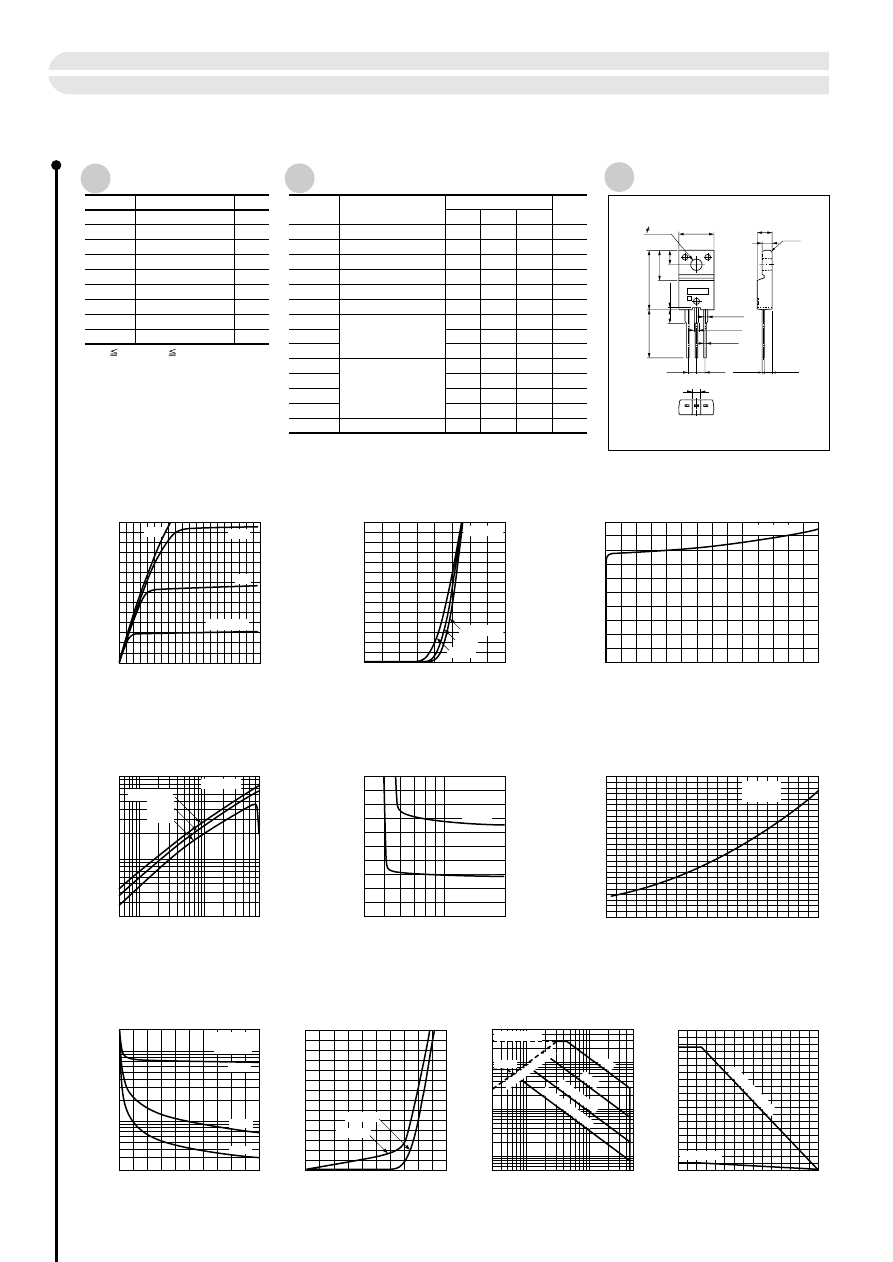
Symbol
Ratings
Unit
(Ta=25ºC)
(Ta=25ºC)
V
DSS
450
Symbol
Test Conditions
Ratings
Unit
V
(BR) DSS
I
D
= 100
µ
A, V
GS
= 0V
450
min
typ
max
I
GSS
nA
µ
A
V
GS
=
±
30V
±
100
I
DSS
S
V
V
DS
= 450V, V
GS
= 0V
100
V
TH
V
DS
= 10V, I
D
= 1mA
4.0
2.0
3.0
5
Re
(yfs)
V
DS
= 20V, I
D
= 3.5A
V
DS
= 10V, I
D
= 3.5A
3.5
R
DS (ON)
Ω
V
ns
ns
ns
ns
V
Coss
Ciss
V
DS
= 10V
f = 1.0MHz
V
GS
= 0V
Crss
t
d (on)
I
D
= 3.5A
V
DD
= 200V
R
L
= 57
Ω
V
GS
= 10V
t
r
t
d (off)
t
f
V
SD
I
SD
= 7A, V
GS
= 0V
0.84
1.10
pF
pF
pF
720
150
65
25
40
70
50
1.0
1.5
V
GSS
V
V
±
30
±
7
±
28
I
D
I
D (pulse)
*
1
A
A
A
35 (Tc=25ºC)
P
T
I
AS
Tch
W
150
7
E
AS
*
2
130
Tstg
ºC
ºC
mJ
–55 to +150
*1 P
W
100
µ
s, duty 1%
*2 V
DD
= 30V, L = 5mH, I
L
= 7A, unclamped, R
G
= 50
Ω
0
10
20
7
1
0
Drain-source voltage V
DS
(V)
Drain current
I
D
(A)
■
I
D
— V
DS
Characteristics
4
5
6
2
3
5
15
5.5V
5V
V
GS
= 10V
0
0
1
7
4
5
6
0.4
0.6
0.8
0.2
1.0
–50
0
0
50
100
150
0.5
1.0
2.0
1.5
2.5
4
1
5
10
20
0
2
7
6
5
4
V
DS
= 20V
25ºC
125ºC
0
20
40
0
50
100
150
0
2
4
6
8
0
2
4
6
10
■
R
DS (ON)
— I
D
Characteristics
■
R
DS (ON)
— T
C
Characteristics
Drain current I
D
(A)
DC ON resistance R
DS (ON)
(
Ω
)
DC ON resistance R
DS (ON)
(
Ω
)
Case temperature Tc (ºC)
■
I
D
— V
GS
Characteristics
■
V
DS
— V
GS
Characteristics
Drain current
I
D
(A)
Gate-source voltage V
GS
(V)
■
P
D
— T
a
Derating
Max. power dissipation
P
D
(W)
Ambient temperature T
a
(ºC)
Gate-source voltage V
GS
(V)
Drain-source voltage
V
DS
(V)
T
C
= –55ºC
10V
3
2
3
0.05
0.2
0.1
0.5
1
0.5
1
10
■
Re
(yfs) — I
D
Characteristics
Drain current I
D
(A)
DC transconductance Re
(yfs)
(S)
5
5 7
8
30
10
V
GS
=
4.5V
25ºC
125ºC
V
DS
=
20V
T
C
= –
55ºC
I
D
= 7A
I
D
= 3.5A
I
D
= 3.5A
V
GS
= 10V
0
10
20
30
40
50
20
50
100
500
1000
2000
Ciss
Coss
Crss
■
Capacitance — V
DS
Characteristics
Drain-source voltage V
DS
(V)
Capacitance Capacitance (pF)
V
GS
=
0V
f
=
1MHz
0
0
0.2
0.4
0.6
0.8
1.0
2
7
6
5
4
Drain reverse current
I
DR
(A)
Source-drain voltage V
SD
(V)
■
I
DR
— V
SD
Characteristics
3
1
5V, 10V
V
GS
= 0V
3
5
10
50
100
500
0.05
0.1
0.5
1
5
10
50
I
D
(pulse) max
I
D
max
10
0
µ
s
DC OPERATION
R
DS
(O
N)
LIMITED
Drain current
I
D
(A)
Drain-source voltage V
DS
(V)
■
Safe Operating Area
(single pulse)
1ms
10
ms (1shot)
(Tc=25ºC)
W
ith infinite heatsink
Without heatsink
Absolute Maximum Ratings
Electrical Characteristics
MOS FET 2SK2701
92
a) Part No.
b) Lot No.
(Unit: mm)
External Dimensions
FM20 (full-mold)
G D S
13.0
min
a
b
3.3
±
0.2
10.0
±
0.2
4.0
±
0.2
8.4
±
0.2
0.8
±
0.2
3.9
±
0.2
1.35
±
0.15
1.35
±
0.15
0.85
2.54
2.54
0.45
2.4
±
0.2
4.2
±
0.2
C 0.5
2.8
16.9
±
0.3
+0.2
–0.1
+0.2
–0.1
2.2
±
0.2
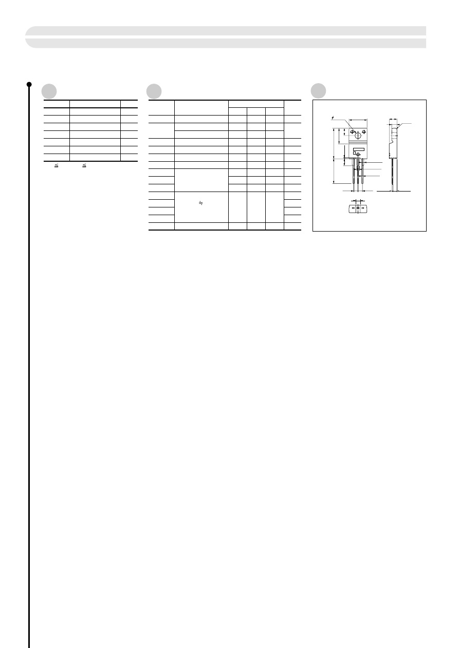
Symbol
Ratings
Unit
(Ta=25ºC)
(Ta=25ºC)
V
DSS
40
Symbol
Test Conditions
Ratings
Unit
V
(BR) DSS
I
D
= 100
µ
A, V
GS
= 0V
40
min
typ
max
I
GSS
µ
A
µ
A
V
GS
= +20V
V
GS
= –10V
+10
–5
I
DSS
S
V
V
DS
= 40V, V
GS
= 0V
100
V
TH
V
DS
= 10V, I
D
= 250
µ
A
2.3
1.3
Re
(yfs)
V
DS
= 10V, I
D
= 25A
20
R
DS (ON)
m
Ω
V
ns
ns
ns
ns
V
V
GS
= 10V, I
D
= 25A
Coss
Ciss
V
DS
= 10V
f = 1.0MHz
V
GS
= 0V
Crss
t
d (on)
I
D
= 25A
V
DD
12V
R
L
= 0.48
Ω
V
GS
= 10V
t
r
t
d (off)
t
f
V
SD
I
SD
= 50A, V
GS
= 0V
6
9
pF
pF
pF
2000
1200
200
1.0
1.5
To be
defined
V
GSS
V
V
+20, –10
±
60
±
180
I
D
A
I
D (pulse)
*
A
40 (Tc=25ºC)
P
D
Tch
W
150
Tstg
ºC
ºC
–55 to +150
* P
W
100
µ
s, duty 1%
Absolute Maximum Ratings
Electrical Characteristics
MOS FET FKV460
(under development)
93
a) Part No.
b) Lot No.
(Unit: mm)
External Dimensions
TO220F (full-mold)
G D S
13.0
min
a
b
3.3
±
0.2
10.0
±
0.2
4.0
±
0.2
8.4
±
0.2
0.8
±
0.2
3.9
±
0.2
1.35
±
0.15
1.35
±
0.15
0.85
2.54
2.54
0.45
2.4
±
0.2
4.2
±
0.2
C 0.5
2.8
16.9
±
0.3
+0.2
–0.1
+0.2
–0.1
2.2
±
0.2
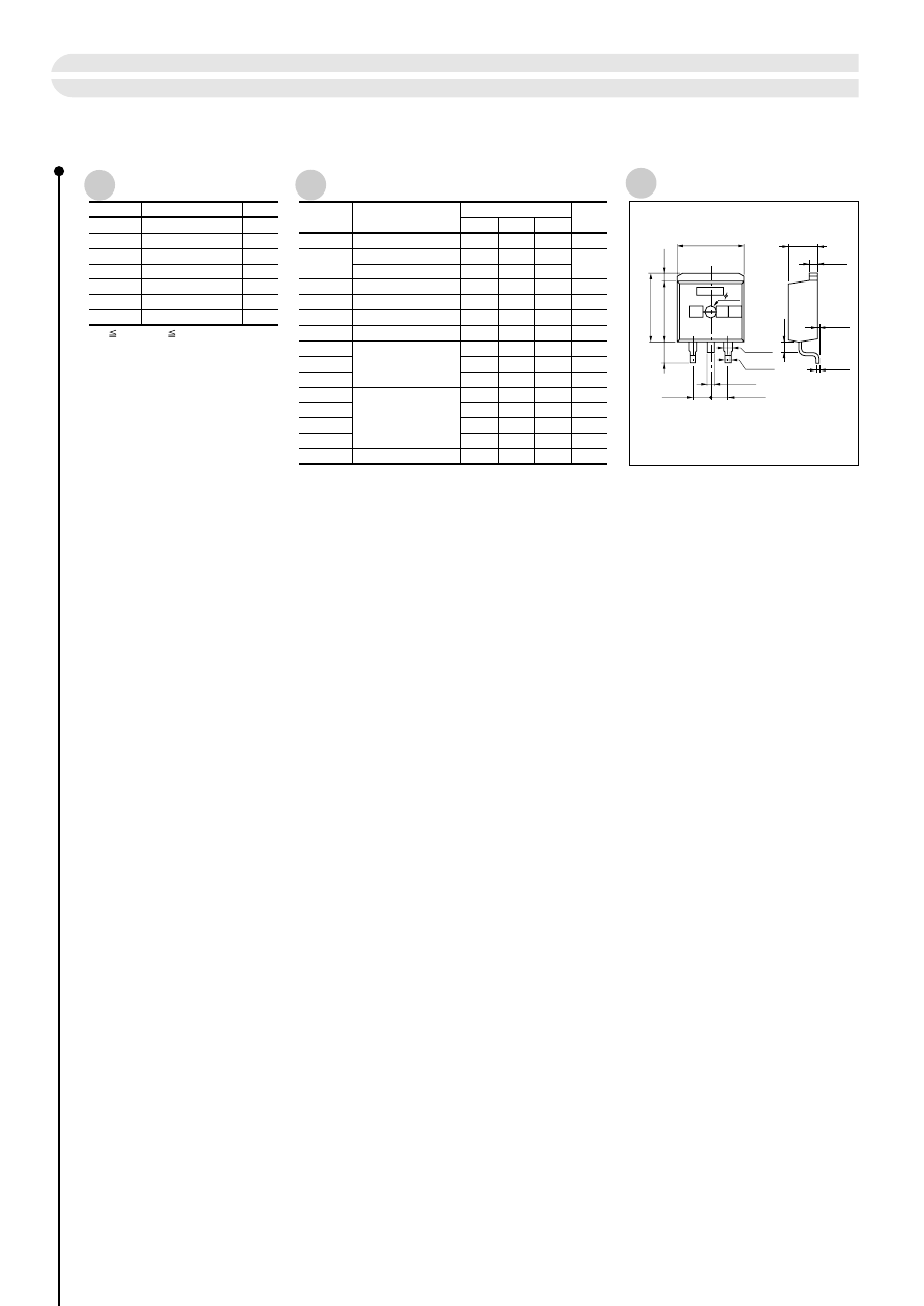
Symbol
Ratings
Unit
(Ta=25ºC)
(Ta=25ºC)
V
DSS
40
Symbol
Test Conditions
Ratings
Unit
V
(BR) DSS
I
D
= 100
µ
A, V
GS
= 0V
40
min
typ
max
I
GSS
µ
A
µ
A
V
GS
= +20V
+10
V
GS
= –10V
–5
I
DSS
S
V
V
DS
= 40V, V
GS
= 0V
100
V
TH
V
DS
= 10V, I
D
= 250
µ
A
2.3
1.3
Re
(yfs)
V
DS
= 10V, I
D
= 25A
20.0
R
DS (ON)
m
Ω
V
ns
ns
ns
ns
V
V
GS
= 10V, I
D
= 25A
Coss
Ciss
V
DS
= 10V
f = 1.0MHz
V
GS
= 0V
Crss
t
d (on)
I
D
= 25A
V
DD
= 12V
R
L
= 0.48
Ω
V
GS
= 10V
t
r
t
d (off)
t
f
V
SD
I
SD
= 50A, V
GS
= 0V
7
9
pF
pF
pF
2800
1400
600
20
600
250
100
1.0
1.5
V
GSS
V
V
+20, –10
±
60
±
180
I
D
A
I
D (pulse)
*
A
60 (Tc=25ºC)
P
D
Tch
W
150
Tstg
ºC
ºC
–55 to +150
* P
W
100
µ
s, duty 1%
Absolute Maximum Ratings
Electrical Characteristics
MOS FET FKV460S
94
a) Part No.
b) Lot No.
(Unit : mm)
External Dimensions
TO220S
a
b
10.2
±
0.3
1.27
±
0.2
2.54
±
0.5
2.54
±
0.5
1.2
±
0.2
1.6
10.0
8.6
±
0.3
(1.4)
–
0.5
+0.3
–
0.5
+0.3
3.0
0.86
4.44
±
0.2
1.3
±
0.2
0.4
±
0.1
(1.5)
0.1
–0.1
+0.2
–0.1
+0.2
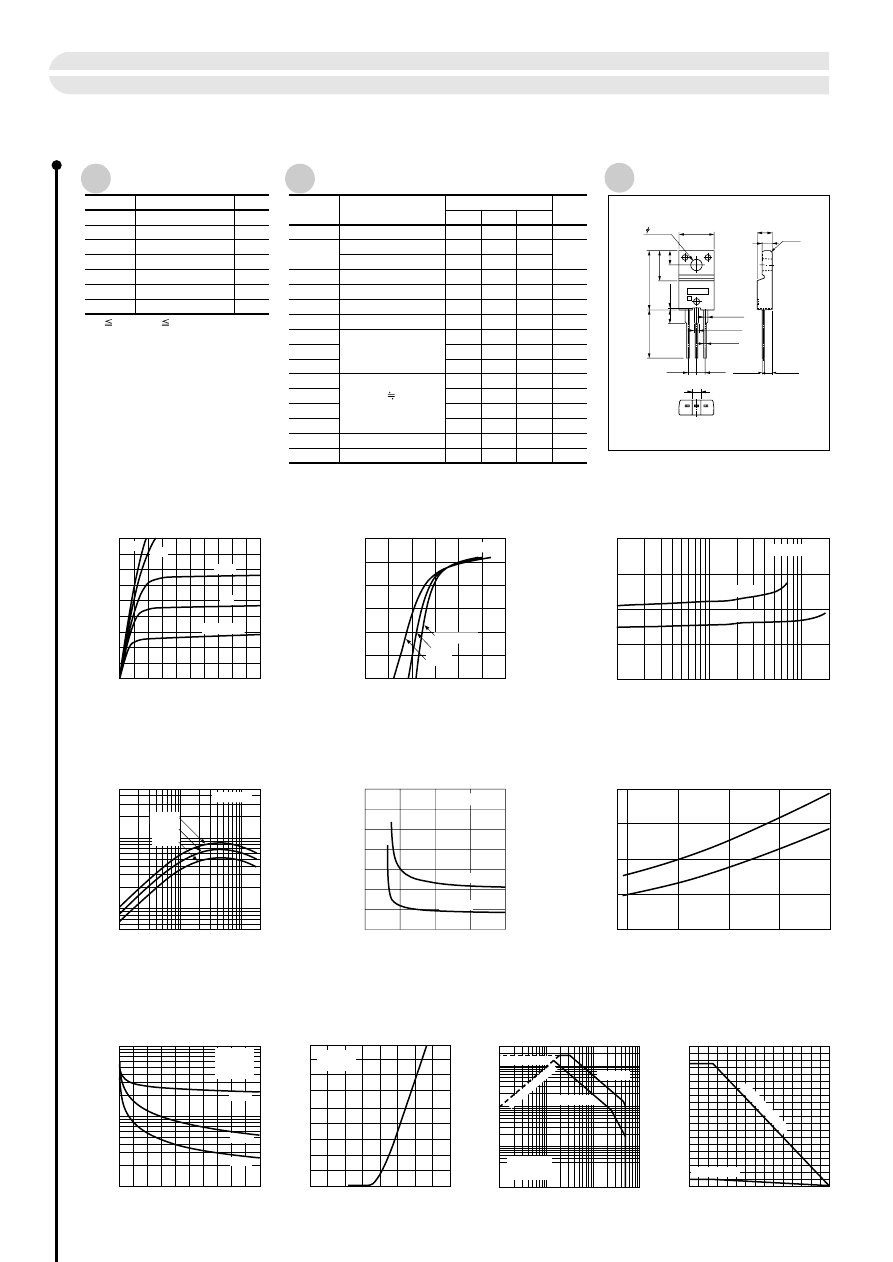
Absolute Maximum Ratings
Electrical Characteristics
Symbol
Ratings
Unit
(Ta=25ºC)
(Ta=25ºC)
V
DSS
50
Symbol
Test Conditions
Ratings
Unit
V
(BR) DSS
I
D
= 100
µ
A, V
GS
= 0V
50
min
typ
max
I
GSS
µ
A
µ
A
V
GS
= +20V
+10
I
DSS
S
V
V
DS
= 50V, V
GS
= 0V
100
V
TH
V
DS
= 10V, I
D
= 250
µ
A
2.5
1.0
Re
(yfs)
V
DS
= 10V, I
D
= 25A
20
R
DS
(ON)
m
Ω
V
ns
ns
ns
ns
V
V
GS
= 10V, I
D
= 25A
Coss
Ciss
V
DS
= 10V
f = 1.0MHz
V
GS
= 0V
Crss
t
d
(on)
I
D
= 25A
V
DD
12V
R
L
= 0.48
Ω
V
GS
= 10V
t
r
t
d
(off)
t
f
V
SD
I
SD
= 50A, V
GS
= 0V
9
11
pF
pF
pF
2700
1100
500
20
600
300
100
1.0
1.5
V
GSS
V
V
+20, –10
±
60
±
180
I
D
A
I
D (pulse)
*
A
35 (Tc=25ºC)
P
D
Tch
W
150
Tstg
ºC
ºC
–55 to +150
V
GS
= –10V
–5
MOS FET FKV560
95
a) Part No.
b) Lot No.
(Unit: mm)
External Dimensions
TO220F (full-mold)
G D S
13.0
min
a
b
3.3
±
0.2
10.0
±
0.2
4.0
±
0.2
8.4
±
0.2
0.8
±
0.2
3.9
±
0.2
1.35
±
0.15
1.35
±
0.15
0.85
2.54
2.54
0.45
2.4
±
0.2
4.2
±
0.2
C 0.5
2.8
16.9
±
0.3
+0.2
–0.1
+0.2
–0.1
2.2
±
0.2
* P
W
100
µ
s, duty 1%
ns
Di, t
rr
I
F
= 25A, di/dt = 100A/
µ
s
110
0
6
4
10
180
20
0
Drain-source voltage V
DS
(V)
Drain current
I
D
(A)
■
I
D
— V
DS
Characteristics
80
100
120
140
160
40
60
2
8
4.5V
4V
Ta=25ºC
0
1
100
200
10
5
10
15
20
–60 –50
0
0
50
100
150
5
10
15
20
0
0.01
5
10
15
20
0.001
0.1
1000
100
10
V
DS
=10V
25ºC
150ºC
0
20
40
0
50
100
150
0
2
4
6
1
3
5
0
0.2
0.4
0.6
0.8
1.0
1.2
1.4
■
R
DS (ON)
— I
D
Characteristics
■
R
DS (ON)
— T
C
Characteristics
Drain current I
D
(A)
DC ON resistance R
DS (ON)
(m
Ω
)
DC ON resistance R
DS (ON)
(m
Ω
)
Case temperature Tc (ºC)
■
I
D
— V
GS
Characteristics
■
V
DS
— V
GS
Characteristics
Drain current
I
D
(A)
Gate-source voltage V
GS
(V)
■
P
D
— T
a
Derating
Max. power dissipation
P
D
(W)
Ambient temperature T
a
(ºC)
Gate-source voltage V
GS
(V)
Drain-source voltage
V
DS
(V)
Ta= –55ºC
10V
6V
1
1
10
100 200
500
■
Re
(yfs) — I
D
Characteristics
Drain current I
D
(A)
DC transconductance Re
(yfs)
(S)
5
10
100
30
10
V
GS
=3.5V
25ºC
125ºC
V
DS
=10V
–55ºC
I
D
=25A
0
10
20
30
40
50
100
1000
10000
Ciss
Coss
Crss
■
Capacitance — V
DS
Characteristics
Drain-source voltage V
DS
(V)
Capacitance Capacitance (pF)
0
0
0.2 0.4
0.6 0.8 1.0 1.2 1.4 1.6
Drain reverse current
I
DR
(A)
Source-drain voltage V
SD
(V)
■
I
DR
— V
SD
Characteristics
20
40
60
80
100
120
140
160
180
0.1
1
10
100
0.1
1
10
300
100
Drain current
I
D
(A)
Drain-source voltage V
DS
(V)
■
Safe Operating Area
W
ith infinite heatsink
Without heatsink
I
D
=60A
I
D
=25A
Ta=25ºC
V
GS
=4V
V
GS
=10V
f=1MHz
V
GS
=0V
Ta= 25ºC
V
GS
= 0V
Ta= 25ºC
I
D
(pulse) max
R
DS (ON)
LIMITED
PT=1ms
PT=10ms
Ta=25ºC
single pulse
V
GS
=4V
V
GS
=10V
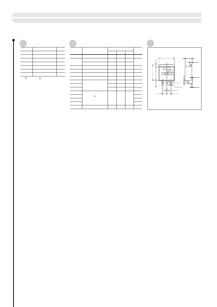
Absolute Maximum Ratings
Electrical Characteristics
Symbol
Ratings
Unit
(Ta=25ºC)
(Ta=25ºC)
V
DSS
50
Symbol
Test Conditions
Ratings
Unit
V
(BR) DSS
I
D
= 100
µ
A, V
GS
= 0V
50
min
typ
max
I
GSS
µ
A
µ
A
V
GS
= +20V
+10
I
DSS
S
V
V
DS
= 50V, V
GS
= 0V
100
V
TH
V
DS
= 10V, I
D
= 250
µ
A
2.0
1.0
Re
(yfs)
V
DS
= 10V, I
D
= 25A
20.0
R
DS
(ON)
m
Ω
V
ns
ns
ns
ns
V
V
GS
= 10V, I
D
= 25A
Coss
Ciss
V
DS
= 10V
f = 1.0MHz
V
GS
= 0V
Crss
t
d
(on)
I
D
= 25A
V
DD
12V
R
L
= 0.48
Ω
V
GS
= 10V
t
r
t
d
(off)
t
f
V
SD
I
SD
= 50A, V
GS
= 0V
9
11
pF
pF
pF
2000
1000
150
1.0
1.5
To be
defined
V
GSS
V
V
±
20
±
45
±
135
I
D
A
I
D (pulse)
*
A
60 (Tc=25ºC)
P
D
Tch
W
150
Tstg
ºC
ºC
–55 to +150
V
GS
= –20V
–5
MOS FET FKV560S
96
External Dimensions
TO220S
a
b
10.2
±
0.3
1.27
±
0.2
2.54
±
0.5
2.54
±
0.5
1.2
±
0.2
1.6
10.0
8.6
±
0.3
(1.4)
3.0
0.86
4.44
±
0.2
1.3
±
0.2
0.4
±
0.1
(1.5)
0.1
a) Part No.
b) Lot No.
(Unit : mm)
* P
W
100
µ
s, duty 1%
+0.2
–0.1
+0.2
–0.1
+0.3 –
0.5
+0.3 –
0.5
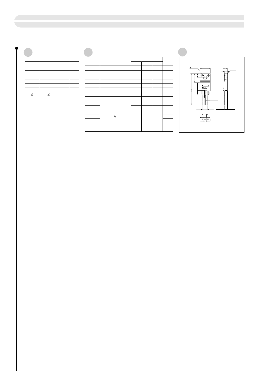
Symbol
Ratings
Unit
(Ta=25ºC)
(Ta=25ºC)
V
DSS
60
Symbol
Test Conditions
Ratings
Unit
V
(BR) DSS
I
D
= 100
µ
A, V
GS
= 0V
60
min
typ
max
I
GSS
µ
A
µ
A
V
GS
= +20V
+10
I
DSS
S
V
V
DS
= 60V, V
GS
= 0V
100
V
TH
V
DS
= 10V, I
D
= 250
µ
A
2.0
1.0
Re
(yfs)
V
DS
= 10V, I
D
= 25A
20.0
R
DS
(ON)
m
Ω
V
ns
ns
ns
ns
V
V
GS
= 10V, I
D
= 25A
Coss
Ciss
V
DS
= 10V
f = 1.0MHz
V
GS
= 0V
Crss
t
d
(on)
I
D
= 25A
V
DD
12V
R
L
= 0.48
Ω
V
GS
= 10V
t
r
t
d
(off)
t
f
V
SD
I
SD
= 50A, V
GS
= 0V
11
14
pF
pF
pF
2000
900
100
1.0
1.5
To be
defined
V
GSS
V
V
±
20
±
50
±
150
I
D
A
I
D (pulse)
*
A
40 (Tc=25ºC)
P
D
Tch
W
150
Tstg
ºC
ºC
–55 to +150
V
GS
= –20V
–5
Absolute Maximum Ratings
Electrical Characteristics
MOS FET FKV660
(under development)
97
a) Part No.
b) Lot No.
(Unit: mm)
External Dimensions
FM20 (full-mold)
C 0.5
G D S
13.0
min
a
b
3.3
±
0.2
10.0
±
0.2
4.0
±
0.2
8.4
±
0.2
0.8
±
0.2
3.9
±
0.2
1.35
±
0.15
1.35
±
0.15
0.85
2.54
2.54
0.45
2.4
±
0.2
4.2
±
0.2
2.8
16.9
±
0.3
2.2
±
0.2
* P
W
100
µ
s, duty 1%
+0.2
–0.1
+0.2
–0.1
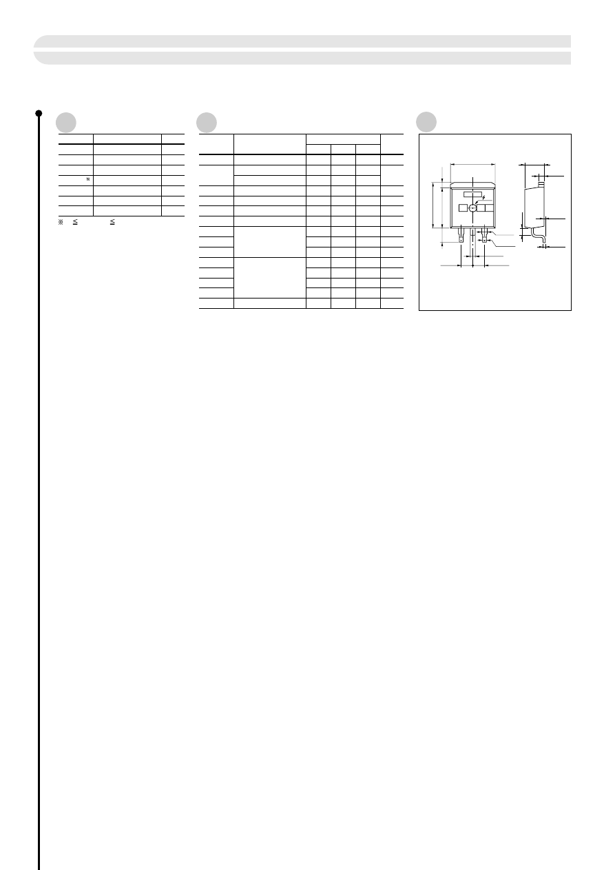
Absolute Maximum Ratings
Electrical Characteristics
Symbol
Ratings
Unit
(Ta=25ºC)
( Ta=25ºC)
V
DSS
60
Symbol
Test Conditions
Ratings
Unit
V
(BR)DSS
I
D
=100
µ
A, V
GS
=0V
60
min
typ
max
I
GSS
µ
A
µ
A
V
GS
=+20V
V
GS
=–10V
+10
– 5
I
DSS
S
V
V
DS
=60V, V
GS
=0V
100
V
TH
V
DS
=10V, I
D
=250
µ
A
2.5
1.0
Re
(yfs)
V
DS
=10V, I
D
=25A
20
R
DS (ON)
m
Ω
V
ns
ns
ns
ns
V
V
GS
=10V, I
D
=25A
Coss
Ciss
V
DS
=10V
f=1.0MHz
V
GS
=0V
Crss
t
d (on)
I
D
=25A
V
DD
=12V
R
L
=0.48
Ω
V
GS
=10V
t
r
t
d (off)
t
f
V
SD
I
SD
=50A, V
GS
=0V
11
14
pF
pF
pF
2500
900
150
50
400
400
300
1.0
1.5
V
GSS
V
V
+20, –10
±
60
±
180
I
D
A
I
D(pulse)
A
60(Tc=25ºC)
P
D
Tch
W
150
Tstg
ºC
ºC
–40 to +150
MOS FET FKV660S
98
External Dimensions
TO220S
a
b
10.2
±
0.3
1.27
±
0.2
2.54
±
0.5
2.54
±
0.5
1.2
±
0.2
1.6
10.0
8.6
±
0.3
(1.4)
–
0.5
+0.3
3.0
0.86 –
0.1
+
0.2
4.44
±
0.2
1.3
±
0.2
0.4
±
0.1
(1
.5
)
0.1–
0.1
+
0.2
a) Part No.
b) Lot No.
(Unit : mm)
P
W
100
µ
s, duty 1%
–
0.5
+0.3
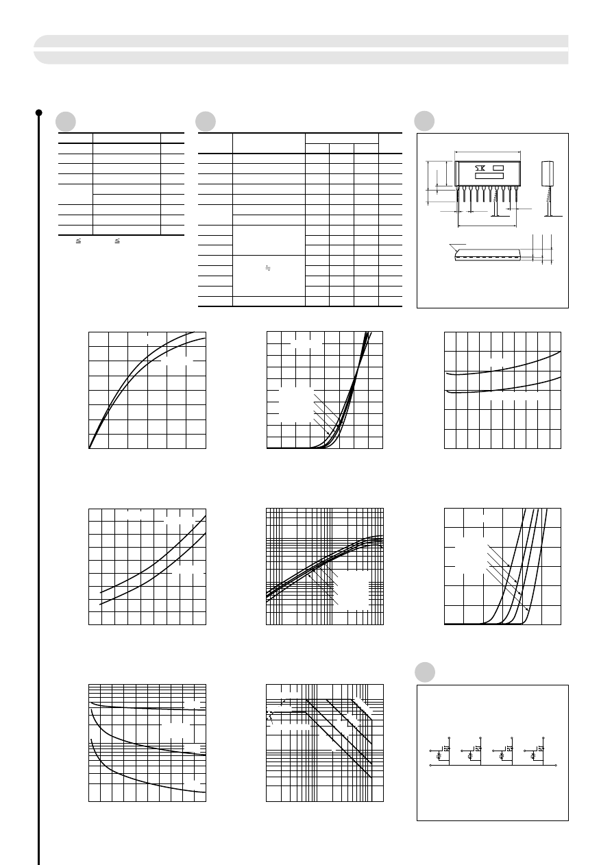
0
1
2
5
3
4
6
■
I
D
—
V
DS
Characteristics
0
12
I
D
(A)
V
DS
(V)
8
4
16
0
8
6
4
2
10
0
1.0
2.0
3.0
4.0
■
I
D
—
V
GS
Characteristics
I
D
(A)
V
GS
(V)
0
2
4
8
6
10
■
R
DS (ON)
—
I
D
Characteristics
0
0.10
0.05
R
DS (ON)
(
Ω
)
I
D
(A)
0.30
0.25
0.20
0.15
–50
0
50
100
150
■
R
DS (ON)
—
T
C
Characteristics
0
0.10
0.30
0.20
0.40
R
DS (ON)
(
Ω
)
Tc
(ºC)
0.45
0
10
20
30
40
50
■
Capacitance
—
V
DS
Characteristics
10
50
100
500
Capacitance
(pF)
V
DS
(V)
1000
1
5
10
50
100 200
■
S
afe Operating Area (single pulse)
0.5
0.1
10
1
5
I
D
(A)
V
DS
(V)
20
(Ta = 25ºC)
0.05
0.1
0.5
1
5
10
■
R
e (yfs) —
I
D
Characteristics
0.1
0.5
1
5
10
50
R
e
(yfs)
(S)
I
D
(A)
V
GS
= 4.5V
V
GS
= 10V
V
GS
= 4V
I
D
= 4A
V
GS
= 10V
V
GS
= 0V
f = 1MHz
Coss
Ciss
Crss
V
DS
= 10V
0
0.4
0.2
0.6
0.8
1.2
1.0
■
I
DR
—
V
SD
Characteristics
0
5
4
3
2
1
I
DR
(A)
V
SD
(V)
6
V
GS
= 4V
V
GS
= 10V
Ta = –55ºC
25ºC
75ºC
150ºC
100ms
10ms
1ms
100
µ
s
I
D
(pulse) max
I
D
(
DC
) max
R
DS
(on) LIMITED
Ta = –55ºC
25ºC
75ºC
150ºC
Ta = 150ºC
75ºC
25ºC
–55ºC
V
GS
= 0V
Symbol
Ratings
Unit
(Ta=25ºC)
(Ta=25ºC)
V
DSS
120
Symbol
Test Conditions
Ratings
Unit
V
(BR) DSS
I
D
= 100
µ
A, V
GS
= 0V
120
min
typ
max
I
GSS
µ
A
µ
A
V
GS
=
±
20V
±
5
I
DSS
S
V
V
DS
= 120V, V
GS
= 0V
100
V
TH
V
DS
= 10V, I
D
= 250
µ
A
2.0
1.0
Re
(yfs)
V
DS
= 10V, I
D
= 4.0A
V
GS
= 10V, I
D
= 4.0A
5.0
R
DS
(ON)
Ω
Ω
V
ns
ns
ns
ns
V
V
GS
= 4V, I
D
= 4.0A
Coss
Ciss
V
DS
= 10V
f = 1.0MHz
V
GS
= 0V
Crss
t
d
(on)
I
D
= 4A
V
DD
12V
R
L
= 3
Ω
V
GS
= 5V
R
G
= 50
Ω
t
r
t
d
(off)
t
f
V
SD
I
SD
= 6A, V
GS
= 0V
0.15
0.2
0.2
0.25
pF
pF
pF
400
130
30
100
300
250
200
1.0
1.5
V
GSS
V
V
±
20
±
6
±
10
I
D
A
I
D (pulse)
*
1
A
4 (Ta = 25ºC)
20 (Tc = 25ºC)
P
T
E
AS
*
2
Tch
W
W
150
80
Tstg
ºC
ºC
mJ
–55 to +150
*1 P
W
100
µ
s, duty 1%
*2 V
DD
= 12V, L = 10mH, unclamped, R
G
= 50
Ω
Electrical Characteristics
Absolute Maximum Ratings
2
1
3
4
5
6
7
8
9
10
MOS FET Array STA508A
99
Equivalent Circuit Diagram
a) Part No.
b) Lot No.
(Unit: mm)
9 •2.54=22.86
±
0.05
a
b
(2.54)
25.25
±
0.2
9.0
±
0.2
2.3
±
0.2
11.3
±
0.2
3.
5
±
0.5
0.5
±
0.15
0
±
0.3
1.0
±
0.25
C1.5
±
0.5
4.0
±
0.2
0.5
±
0.15
1.2
±
0.2
1
3
2
4
S G D G
5
6
7
10
D
G D
S
8
9
G D
0
±
0.3
External Dimensions
STA4 (LF412)
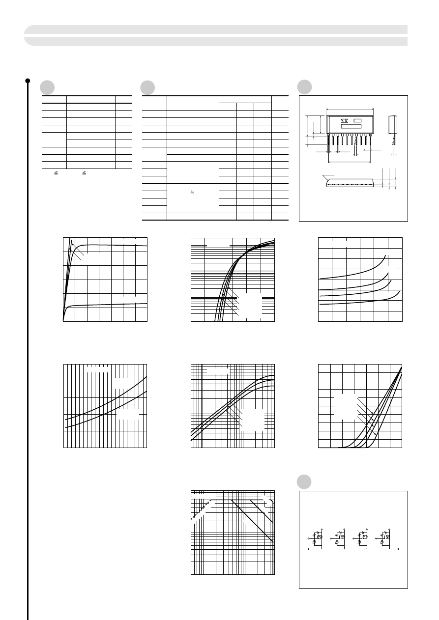
0
2
4
10
12
6
8
14
■
I
D
—
V
DS
Characteristics
0
5
4
I
D
(A)
V
DS
(V)
3
2
1
6
0.01
1
0.1
20
10
0
1
2
3
4
5
6
■
I
D
—
V
GS
Characteristics
I
D
(A)
V
GS
(V)
0
1
2
3
6
4
5
■
R
DS (ON)
—
I
D
Characteristics
0
0.2
R
DS (ON)
(
Ω
)
I
D
(A)
0.8
0.6
0.4
–50
0
50
100
150
■
R
DS (ON)
—
T
C
Characteristics
0
0.1
0.3
0.2
0.4
R
DS (ON)
(
Ω
)
Tc (ºC)
0.5
0.5
1
5
10
50
■
Safe Operating Area (single pulse)
0.5
0.1
1
5
I
D
(A)
V
DS
(V)
10
(Tc = 25ºC)
0.05
0.1
0.5
1
6
■
R
e (yfs) —
I
D
Characteristics
0.2
0.5
1
5
10
R
e
(yfs)
(S)
I
D
(A)
V
GS
= 3V
V
GS
= 4V
V
GS
= 5V
V
GS
= 10V
V
GS
= 4V
typ.
I
D
= 1A
V
GS
= 10V
typ.
V
DS
= 10V
V
DS
= 10V
V
GS
= 4V
0
0.4
0.2
0.6
0.8
1.4
1.2
1.0
■
I
DR
—
V
SD
Characteristics
0
8
6
4
2
I
DR
(A)
V
SD
(V)
10
Ta = –55ºC
25ºC
75ºC
150ºC
10ms
1ms
100
µ
s
I
D
(pulse) max
R
DS
(o
n)
LIM
ITED
Ta = –55ºC
25ºC
150ºC
Ta = 150ºC
75ºC
25ºC
–55ºC
25ºC
Ta = 150ºC
75ºC
–55ºC
Symbol
Ratings
Unit
(Ta=25ºC)
(Ta=25ºC)
V
DSS
52
±
5
Symbol
Test Conditions
Ratings
Unit
V
(BR) DSS
I
D
= 1mA, V
GS
= 0V
47
52
57
min
typ
max
I
GSS
µ
A
µ
A
V
GS
=
±
20V
±
1.0
I
DSS
S
V
V
DS
= 40V, V
GS
= 0V
100
V
TH
V
DS
= 10V, I
D
= 250
µ
A
2.5
1.0
Re
(yfs)
V
DS
= 10V, I
D
= 1.0A
V
GS
= 10V, I
D
= 1.0A
1.0
R
DS
(ON)
Ω
Ω
V
µ
s
µ
s
µ
s
µ
s
V
V
GS
= 4V, I
D
= 1.0A
Coss
Ciss
V
DS
= 10V
f = 1.0MHz
V
GS
= 0V
Crss
t
d
(on)
I
D
= 1A
V
DD
12V
R
L
= 12
Ω
V
GS
= 5V
R
G1
= 50
Ω
, R
G2
= 10
Ω
t
r
t
d
(off)
t
f
V
SD
I
SD
= 6A, V
GS
= 0V
0.2
0.25
0.25
0.3
pF
pF
pF
200
120
20
2.0
7.4
3.3
4.2
1.0
1.5
V
GSS
V
V
±
20
±
3
±
6
I
D
A
I
D (pulse)
*
1
A
4 (Ta = 25ºC)
20 (Tc = 25ºC)
P
T
E
AS
*
2
Tch
W
W
150
40
Tstg
ºC
ºC
mJ
–55 to +150
*1 P
W
100
µ
s, duty 1%
*2 V
DD
= 12V, L = 10mH, unclamped, R
G
= 10
Ω
Electrical Characteristics
Absolute Maximum Ratings
2
1
3
4
5
6
7
8
9
10
MOS FET Array STA509A
100
Equivalent Circuit Diagram
External Dimensions
STA
a) Part No.
b) Lot No.
(Unit: mm)
9 •2.54=22.86
±
0.05
a
b
(2.54)
25.25
±
0.2
9.0
±
0.2
2.3
±
0.2
11.3
±
0.2
3.
5
±
0.5
0.5
±
0.15
0
±
0.3
1.0
±
0.25
C1.5
±
0.5
4.0
±
0.2
0.5
±
0.15
1.2
±
0.2
1
3
2
4
S G D G
5
6
7
10
D
G D
S
8
9
G D
0
±
0.3
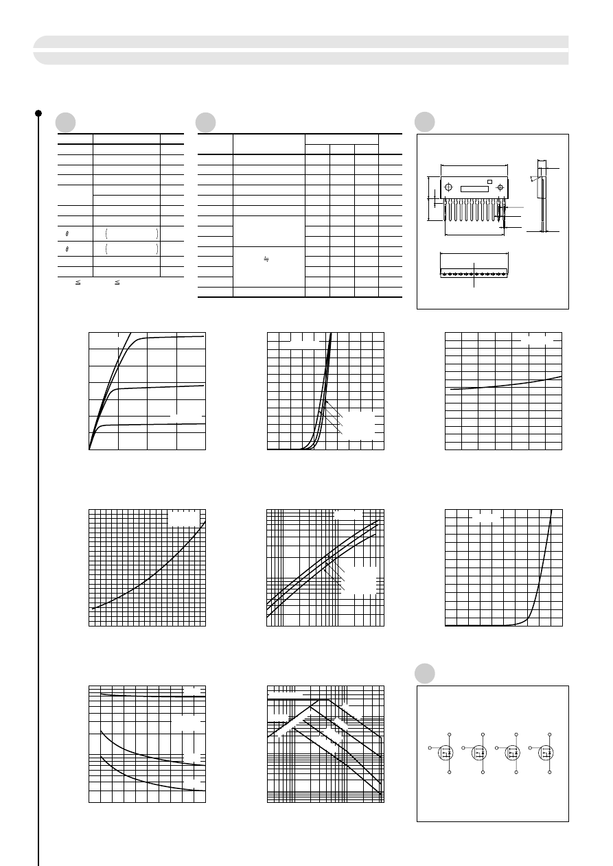
Absolute Maximum Ratings
Electrical Characteristics
0
5
10
15
20
■
I
D
—
V
DS
Characteristics
0
5
6
I
D
(A)
V
DS
(V)
4
3
2
1
7
0
5
6
4
3
2
1
7
0
2
4
6
8
10
■
I
D
—
V
GS
Characteristics
I
D
(A)
V
GS
(V)
0
1
2
3
4
5
6
7
■
R
DS (ON)
—
I
D
Characteristics
0
1.0
0.5
R
DS (ON)
(
Ω
)
I
D
(A)
1.5
–50
0
50
100
150
■
R
DS (ON)
—
T
C
Characteristics
0
1.0
0.5
2.0
1.5
R
D
S (ON)
(
Ω
)
Tc (ºC)
2.5
0
10
20
30
40
50
■
Capacitance — V
DS
Characteristics
20
50
100
500
Capacitance (pF)
V
DS
(V)
1000
3
5
10
50
100
500
■
Safe Operating Area (single pulse)
0.5
0.1
0.05
10
1
5
I
D
(A)
V
DS
(V)
50
(Ta = 25ºC)
0.05
0.1
0.5
1
7
■
R
e (yfs) —
I
D
Characteristics
2
5
10
50
R
e
(yfs)
(S)
I
D
(A)
100
5.5V
5V
V
GS
= 4.5V
I
D
= 3.5A
V
DS
= 20V
V
GS
= 10V
V
GS
= 0V
f = 1MHz
Coss
Ciss
Crss
V
DS
= 20V
0
0.4
0.2
0.6
0.8
1.0
■
I
DR
—
V
SD
Characteristics
0
5
4
3
2
1
6
I
DR
(A)
V
SD
(V)
7
V
GS
= 0V
V
GS
= 10V
Ta = –55ºC
25ºC
150ºC
100ms
10ms
1ms
100
µ
s
I
D
(pulse) max
I
D (DC)
max
R
DS
(o
n)
LIM
ITED
10V
Ta = –55ºC
25ºC
150ºC
Symbol
Ratings
Unit
(Ta=25ºC)
(Ta=25ºC)
V
DSS
450
Symbol
Test Conditions
Ratings
Unit
V
(BR) DSS
I
D
= 100
µ
A, V
GS
= 0V
450
min
typ
max
I
GSS
nA
µ
A
V
GS
=
±
30V
±
100
I
DSS
S
V
V
DS
= 450V, V
GS
= 0V
100
V
TH
V
DS
= 10V, I
D
= 1mA
4.0
5.0
2.0
Re
(yfs)
V
DS
= 20V, I
D
= 3.5A
3.5
R
DS
(ON)
Ω
V
ns
ns
ns
ns
V
V
GS
= 10V, I
D
= 3.5A
Coss
Ciss
V
DS
= 10V
f = 1.0MHz
V
GS
= 0V
Crss
t
d
(on)
I
D
= 3.5A
V
DD
200V
R
L
= 57
Ω
V
GS
= 10V
R
G
= 50
Ω
t
r
t
d
(off)
t
f
V
SD
I
SD
= 7A, V
GS
= 0V
0.84
1.1
pF
pF
pF
720
150
65
25
40
70
50
1.0
1.5
V
GSS
j-a
j-c
I
AS
V
V
±
30
±
7
±
28
I
D
A
I
D (pulse)
*
1
A
A
4 (Ta=25ºC, All circuits operate, No Fin)
35 (Tc=25ºC, All circuits operate,
∞
Fin)
P
T
E
AS
*
2
Tch
W
W
150
130
7
31.2
3.57
Tstg
ºC
ºC
ºC/W
ºC/W
mJ
–55 to +150
*1 P
W
100
µ
s, duty 1%
*2 V
DD
= 30V, L = 5mH, I
L
= 7A, unclamped,
R
G
= 50
Ω
MOS FET Array SMA5113
101
1
3
2
4
6
5
8
7
9
11
10
12
Equivalent Circuit Diagram
Junction - Ambientare,
Ta=25ºC, All circuits operate
Junction - Case,
Ta=25ºC, All circuits operate
0.85
31.5 max
a
b
31.0
±
0.2
4.0
±
0.2
2.5
±
0.2
1.46
±
0.15
1.21
±
0.15
11• P2.54
±
0.1
= 27.94
10.2
±
0.2
2.4
(10.4)
0.55
1.2
±
0.1
30º
1 2 3 4 5 6 7 8 9 10 11 12
a) Part No.
b) Lot No.
(Unit: mm)
External Dimensions
SMA (LF1000)
+0.2
–0.1
+0.2
–0.1
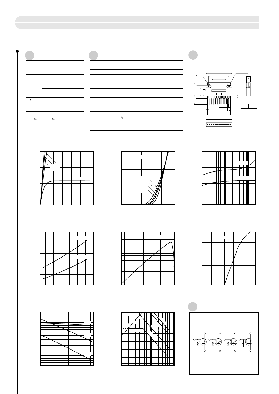
0
1
2
3
4
5
6
■
I
D
—
V
DS
Characteristics
0
4
8
I
D
(A)
V
DS
(V)
6
2
10
0
1
2
3
4
■
I
D
—
V
GS
Characteristics
0
4
6
10
I
D
(A)
V
GS
(V)
8
2
12
0.1
1
10
20
■
R
DS (ON)
—
I
D
Characteristics
0
0.05
R
DS (on)
(
Ω
)
I
D
(A)
0.1
–50
0
50
100
150
■
R
DS (ON)
—
T
C
Characteristics
0.02
0.06
0.10
R
DS (ON)
(
Ω
)
Tc (ºC)
0.12
1
5
10
50
■
Capacitance —
V
DS
Characteristics
50
500
100
1000
Capacitance (pF)
V
DS
(V)
2000
0.5
1
5
10
100
50
■
Safe Operating Area (single pulse)
0.5
10
1
5
I
D
(A)
V
DS
(V)
50
(Ta = 25ºC)
0.4
1
5
10
20
■
R
e (yfs) —
I
D
Characteristics
2
5
10
R
e
(yfs)
(S)
I
D
(A)
30
4V
5V
10V
V
GS
= 3V
V
GS
= 4V
V
DS
= 10V
V
GS
= 10V
V
GS
= 0V
f = 1MHz
Coss
Ciss
Crss
V
DS
= 10V
0
0.4
0.8
1.2
■
I
DR
—
V
SD
Characteristics
0.1
5
10
I
DR
(A)
V
SD
(V)
1
0.5
20
V
GS
= 0V
V
GS
= 4V
V
GS
= 10V
Ta = 150ºC
75ºC
25ºC
–55ºC
100ms
10ms
1ms
0.5ms
I
D
(pulse) max
I
D (DC)
max
R
D
S
(on)
LIM
IT
E
D
Assumed V
G
S
= 4V line
Symbol
Ratings
Unit
(Ta=25ºC)
(Ta=25ºC)
V
DSS
60
Symbol
Test Conditions
Ratings
Unit
V
(BR) DSS
I
D
= 100
µ
A, V
GS
= 0V
60
min
typ
max
I
GSS
µ
A
µ
A
V
GS
=
±
20V
±
100
I
DSS
S
V
V
DS
= 60V, V
GS
= 0V
100
V
TH
V
DS
= 10V, I
D
= 1mA
2.0
1.5
12.0
1.0
Re
(yfs)
V
DS
= 10V, I
D
= 8A
6.0
R
DS
(ON)
Ω
V
ns
ns
ns
ns
V
V
GS
= 4V, I
D
= 8A
Coss
Ciss
V
DS
= 10V
f = 1.0MHz
V
GS
= 0V
Crss
t
d
(on)
I
D
= 8A
V
DD
30V
R
L
= 3.75
Ω
V
GS
= 5V
R
G
= 50
Ω
t
r
t
d
(off)
t
f
V
SD
I
SD
= 10A, V
GS
= 0V
0.07
0.08
pF
pF
pF
1100
500
170
50
250
250
180
1.0
1.5
V
GSS
j-c
V
ISO
V
V
±
20
±
12
±
48
I
D
A
I
D (pulse)
*
1
A
5 (Ta=25ºC, 4 circuits operate)
60 (Tc=25ºC,4 circuits operate)
P
T
E
AS
*
2
Tch
W
W
Vrms
150
250
2.08
(Fin to lead terminal) AC1000
Tstg
ºC
ºC
ºC/W
mJ
–55 to +150
*1 P
W
250
µ
s, duty 1%
*2 V
DD
= 30V, L = 10mH, unclamped, R
G
= 50
Ω
Absolute Maximum Ratings
Electrical Characteristics
1
3
2
4
6
5
8
7
9
11
10
12
MOS FET Array SLA5027
102
1 2 3
11•P2.54
±
0.7
=27.94
±
1.0
31.5 max
0.85
1.2
±
0.15
31.0
±
0.2
24.4
±
0.2
16.4
±
0.2
3.2
±
0.15
0.55
2.2
±
0.7
1.7
±
0.1
4.8
±
0.2
1.45
±
0.15
Pin 1
12
4 5 6 7 8 9 10 11 12
8.5
m
a
x
9
.5
min (10.4)
9.9
±
0.2
13.0
±
0.2
16.0
±
0.2
2.7
a) Part No.
b) Lot No.
(Unit: mm)
External Dimensions
SLA (LF800)
Equivalent Circuit Diagram
a
b
+0.2
–0.1
+0.2
–0.1
Ellipse 3.2
±
0.15
• 3.8
Lead plate thickness
resins
0.8
max
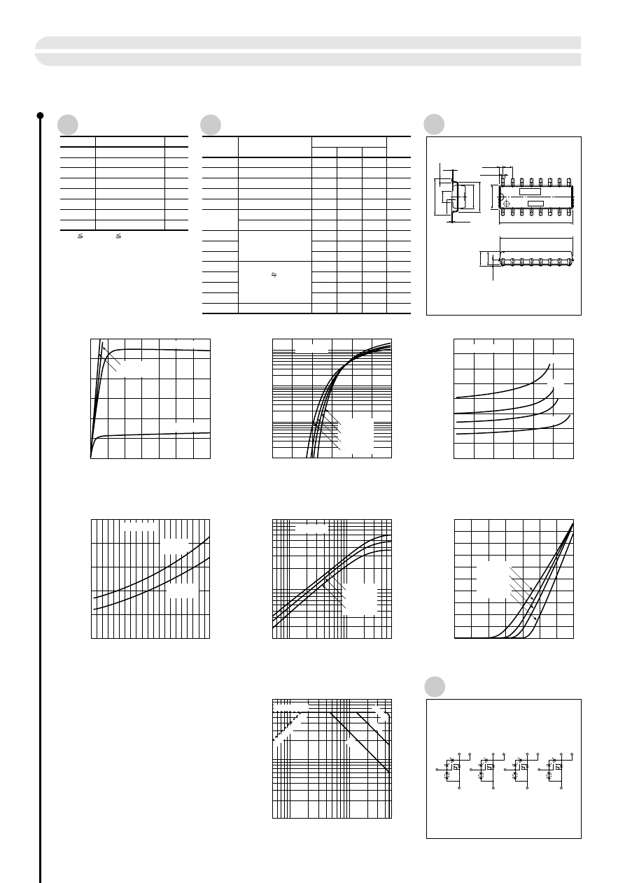
Absolute Maximum Ratings
Electrical Characteristics
Symbol
Ratings
Unit
(Ta=25ºC)
(Ta=25ºC)
V
DSS
52
±
5
Symbol
Test Conditions
Ratings
Unit
V
(BR) DSS
I
D
= 1mA, V
GS
= 0V
47
52
57
min
typ
max
I
GSS
µ
A
µ
A
V
GS
=
±
20V
±
1.0
I
DSS
S
V
V
DS
= 40V, V
GS
= 0V
100
V
TH
V
DS
= 10V, I
D
= 250
µ
A
2.5
1.8
1.0
Re
(yfs)
V
DS
= 10V, I
D
= 1.0A
1.0
R
DS
(ON)
Ω
Ω
V
µ
s
µ
s
µ
s
µ
s
V
V
GS
= 10V, I
D
= 1.0A
V
GS
= 4V, I
D
= 1.0A
Coss
Ciss
V
DS
= 10V
f = 1.0MHz
V
GS
= 0V
Crss
t
d
(on)
I
D
= 1A
V
DD
12V
R
L
= 12
Ω
V
GS
= 5V
R
G1
= 50
Ω
, R
G2
= 10k
Ω
t
r
t
d
(off)
t
f
V
SD
I
SD
= 1A, V
GS
= 0V
0.2
0.25
0.25
0.3
pF
pF
pF
200
120
20
2.0
7.4
3.3
4.2
1.0
1.5
V
GSS
V
V
±
20
±
3
±
6
I
D
A
I
D (pulse)
*
1
A
3 (Tc=25ºC, 4 circuits operate)
P
T
E
AS
*
2
Tch
W
150
40
Tstg
ºC
ºC
mJ
–55 to +150
*1 P
W
100
µ
s, duty 1%
*2 V
DD
= 12V, L = 10mH, unclamped, R
G
= 10
Ω
2
1
15
16
4
3
13
14
6
5
11
12
8
7
9
10
Surface-mount MOS FET Array SDK06
103
Equivalent Circuit Diagram
a) Part No.
b) Lot No.
(Unit: mm)
a
b
20.0max
2.54
±
0.25
0.89
±
0.15
8.0
±
0.5
6.3
±
0.2
0 to 0.15
3.0
±
0.2
0.25
9.8
±
0.3
1.0
±
0.3
19.56
±
0.2
6.8max
0.75
0.3
16
Pin 1
8
9
4.0max
3.6
±
0.2
1.4
±
0.2
External Dimensions
SMD-16A
+0.15
–0.05
+0.15
–0.05
0
2
4
10
12
6
8
14
■
I
D
—
V
DS
Characteristics
0
5
4
I
D
(A)
V
DS
(V)
3
2
1
6
0.01
1
0.1
20
10
0
1
2
3
4
5
6
■
I
D
—
V
GS
Characteristics
I
D
(A)
V
GS
(V)
0
1
2
3
6
4
5
■
R
DS (ON)
—
I
D
Characteristics
0
0.2
R
DS (ON)
(
Ω
)
I
D
(A)
0.8
0.6
0.4
–50
0
50
100
150
■
R
DS (ON)
—
T
C
Characteristics
0
0.1
0.3
0.2
0.4
R
DS (ON)
(
Ω
)
Tc (ºC)
0.5
0.5
1
5
10
50
■
Safe Operating Area (single pulse)
0.5
0.1
1
5
I
D
(A)
V
DS
(V)
10
(Tc = 25ºC)
0.05
0.1
0.5
1
6
■
R
e (yfs) —
I
D
Characteristics
0.2
0.5
1
5
10
R
e
(yfs)
(S)
I
D
(A)
V
GS
= 3V
V
GS
= 4V
V
GS
= 5V
V
GS
= 10V
V
GS
= 4V
typ.
I
D
= 1A
V
GS
= 10V
typ.
V
DS
= 10V
V
DS
= 10V
V
GS
= 4V
0
0.4
0.2
0.6
0.8
1.4
1.2
1.0
■
I
DR
—
V
SD
Characteristics
0
8
6
4
2
I
DR
(A)
V
SD
(V)
10
Ta = –55ºC
25ºC
75ºC
150ºC
10ms
1ms
100
µ
s
I
D
(pulse) max
R
DS
(o
n)
LIM
ITED
Ta = –55ºC
25ºC
150ºC
Ta = 150ºC
75ºC
25ºC
–55ºC
25ºC
Ta = 150ºC
75ºC
–55ºC
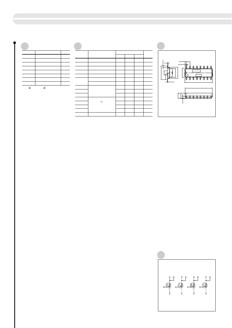
Symbol
Ratings
Unit
(Ta=25ºC)
(Ta=25ºC)
V
DSS
50
Symbol
Test Conditions
Ratings
Unit
V
(BR) DSS
I
D
= 100
µ
A, V
GS
= 0V
50
min
typ
max
I
GSS
nA
µ
A
V
GS
=
±
20V
±
100
I
DSS
S
V
V
DS
= 50V, V
GS
= 0V
100
V
TH
V
DS
= 10V, I
D
= 1mA
2.3
13.0
1.8
9.0
1.3
Re
(yfs)
V
DS
= 10V, I
D
= 4.0A
5.0
R
DS
(ON)
Ω
Ω
V
ns
ns
ns
ns
V
V
GS
= 10V, I
D
= 4.0A
V
GS
= 4V, I
D
= 4.0A
Coss
Ciss
V
DS
= 10V
f = 1.0MHz
V
GS
= 0V
Crss
t
d
(on)
I
D
= 4A
V
DD
12V
R
L
= 3
Ω
V
GS
= 5V
R
G
= 50
Ω
t
r
t
d
(off)
t
f
V
SD
I
SD
= 6A, V
GS
= 0V
0.07
0.08
0.09
0.1
pF
pF
pF
700
300
90
50
80
60
40
1.0
1.5
V
GSS
V
V
±
20
±
4.5
±
9
I
D
A
I
D (pulse)
*
1
A
4 (Tc=25ºC, 4 circuits operate)
P
T
E
AS
*
2
Tch
W
150
80
Tstg
ºC
ºC
mJ
–55 to +150
*1 P
W
100
µ
s, duty 1%
*2 V
DD
= 12V, L = 10mH, unclamped, R
G
= 50
Ω
Absolute Maximum Ratings
Electrical Characteristics
1
15
16
2
3
13
14
4
5
11
12
6
7
9
10
8
Surface-mount MOS FET Array SDK08
104
Equivalent Circuit Diagram
a) Part No.
b) Lot No.
(Unit: mm)
a
b
20.0max
2.54
±
0.25
0.89
±
0.15
8.0
±
0.5
6.3
±
0.2
0 to 0.15
3.0
±
0.2
0.25
9.8
±
0.3
1.0
±
0.3
19.56
±
0.2
6.8max
0.75
0.3
16
Pin 1
8
9
4.0max
3.6
±
0.2
1.4
±
0.2
External Dimensions
SMD-16A
+0.15
–0.05
+0.15
–0.05
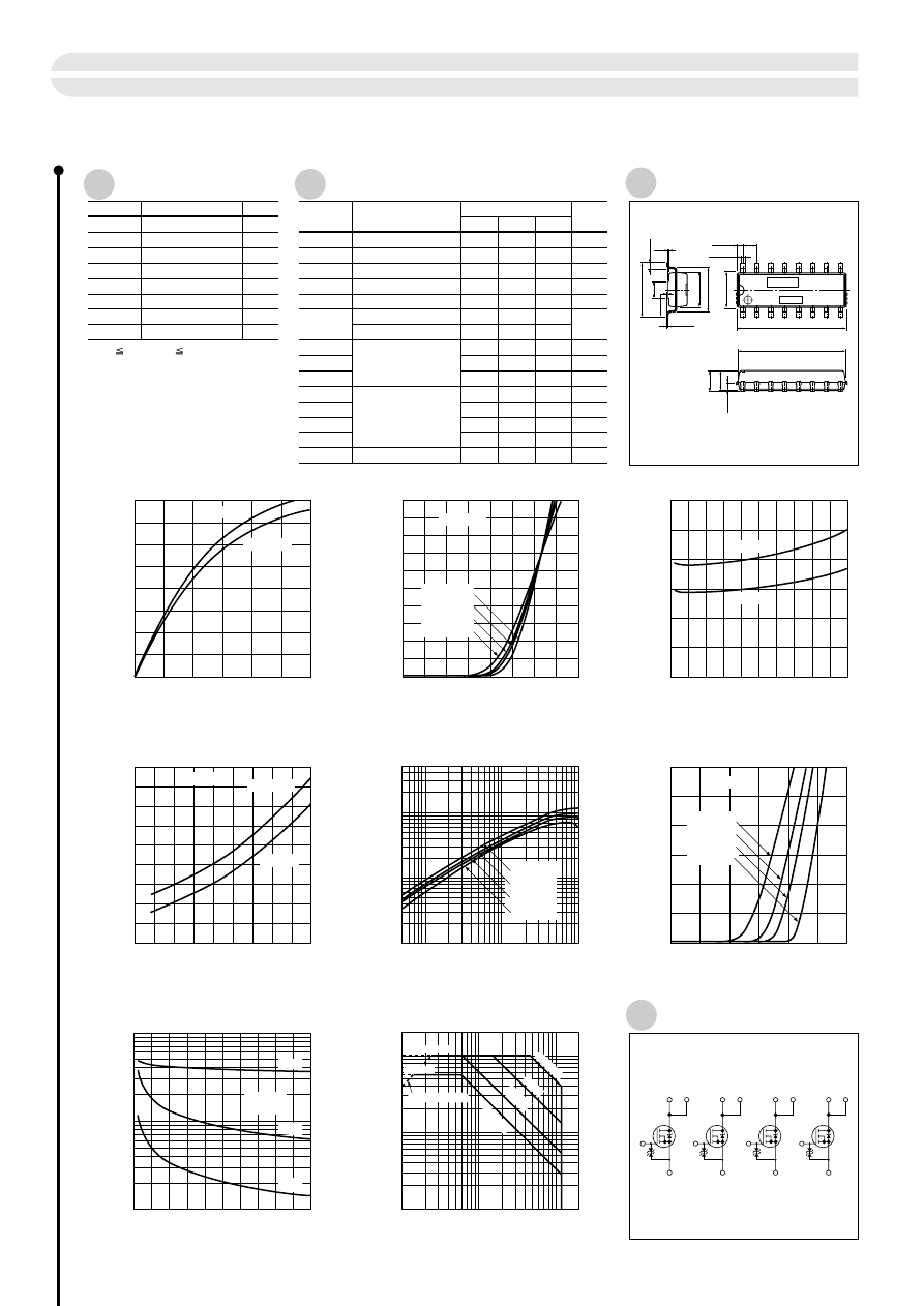
Symbol
Ratings
Unit
(Ta=25ºC)
(Ta=25ºC)
V
DSS
120
Symbol
Test Conditions
Ratings
Unit
V
(BR) DSS
I
D
=100
µ
A, V
GS
=0V
120
min
typ
max
I
GSS
µ
A
µ
A
V
GS
=
±
20V
±
5
I
DSS
S
V
V
DS
=120V, V
GS
=0V
100
V
TH
V
DS
=10V, I
D
=250
µ
A
2.0
1.0
Re
(yfs)
V
DS
=10V, I
D
=4A
5.0
R
DS
(ON)
Ω
V
ns
ns
ns
ns
V
V
GS
=10V, I
D
=4A
V
GS
=4V, I
D
=4A
Coss
Ciss
V
DS
=10V
f=1.0MHz
V
GS
=0V
Crss
t
d
(on)
I
D
=4A
V
DD
=12V
R
L
=3
Ω
V
GS
=5V
R
G
=50
Ω
t
r
t
d
(off)
t
f
V
SD
I
SD
=6A, V
GS
=0V
0.15
0.2
0.2
0.25
pF
pF
pF
400
130
30
100
300
250
200
1.0
1.5
V
GSS
V
V
±
20
±
6
±
10
I
D
A
I
D (pulse)
*
1
A
3 (Tc=25ºC, 4 circuits operate)
P
T
Tch
W
150
Tstg
ºC
ºC
–55 to +150
80
E
AS
*
2
mJ
Absolute Maximum Ratings
Electrical Characteristics
1
15
16
2
3
13
14
4
5
11
12
6
7
9
10
8
Surface-mount MOS FET Array SDK09
(under development)
105
Equivalent Circuit Diagram
a) Part No.
b) Lot No.
(Unit: mm)
a
b
20.0max
2.54
±
0.25
0.89
±
0.15
8.0
±
0.5
6.3
±
0.2
0 to 0.15
3.0
±
0.2
0.25
9.8
±
0.3
1.0
±
0.3
19.56
±
0.2
6.8max
0.75
0.3
+0.15
–0.05
+0.15
–0.05
16
Pin 1
8
9
4.0max
3.6
±
0.2
1.4
±
0.2
External Dimensions
SMD-16A
0
1
2
5
3
4
6
■
I
D
—
V
DS
Characteristics
0
12
I
D
(A)
V
DS
(V)
8
4
16
0
8
6
4
2
10
0
1.0
2.0
3.0
4.0
■
I
D
—
V
GS
Characteristics
I
D
(A)
V
GS
(V)
0
2
4
8
6
10
■
R
DS (ON)
—
I
D
Characteristics
0
0.10
0.05
R
DS (ON)
(
Ω
)
I
D
(A)
0.30
0.25
0.20
0.15
–50
0
50
100
150
■
R
DS (ON)
—
T
C
Characteristics
0
0.10
0.30
0.20
0.40
R
DS (ON)
(
Ω
)
Tc
(ºC)
0.45
0
10
20
30
40
50
■
Capacitance —
V
DS
Characteristics
10
50
100
500
Capacitance
(pF)
V
DS
(V)
1000
1
5
10
50
100 200
■
Safe Operating Area (single pulse)
0.5
0.1
10
1
5
I
D
(A)
V
DS
(V)
20
(Ta = 25ºC)
0.05
0.1
0.5
1
5
10
■
R
e (yfs) —
I
D
Characteristics
0.1
0.5
1
5
10
50
R
e
(yfs)
(S)
I
D
(A)
V
GS
=4.5V
V
GS
=10V
V
GS
=4V
I
D
=4A
V
GS
=10V
V
GS
=0V
f=1MHz
Coss
Ciss
Crss
V
DS
=10V
0
0.4
0.2
0.6
0.8
1.2
1.0
■
I
DR
—
V
SD
Characteristics
0
5
4
3
2
1
I
DR
(A)
V
SD
(V)
6
V
GS
=4V
V
GS
=10V
Ta=–55ºC
25ºC
75ºC
150ºC
100ms
10ms
1ms
100
µ
s
I
D (
pulse) max
I
D (DC)
max
R
DS (
on) LIMITED
Ta=–55ºC
25ºC
75ºC
150ºC
Ta=150ºC
75ºC
25ºC
–55ºC
V
GS
=0V
*1 P
W
100
µ
s, duty 1%
*2 V
DD
= 12V, L = 10mH, unclamped, R
G
= 50
Ω
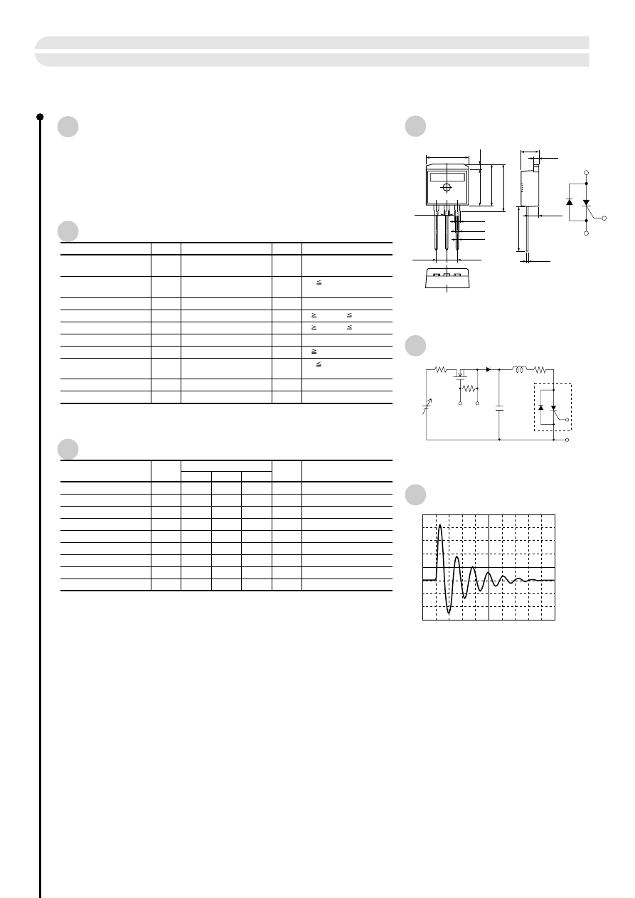
Measurement circuit
Current waveform (1cycle)
External Dimensions
(unit: mm)
Thyristor with built-in reverse diode for HID lamp ignition TFC561D
106
Features
●
Repetitive peak off-state voltage: V
DRM
=600V
●
Repetitive peak surge on-state current: I
TRM
=430A
●
Critical rate-of-rise of on-state current: di/dt=1200A/
µ
s
●
Gate trigger current: I
GT
=20mA max
●
With built-in reverse diode
Parameter
Symbol
Unit
Conditions
Ratings
Absolute Maximum Ratings
Repetitive peak off-state voltage
Repetitive surge peak
on-state current
Critical rate-of-rise of on-state current
Average gate power loss
Peak reverse gate voltage
Diode repetitive peak surge
forward current
Junction temperature
V
DRM
I
TRM
di/dt
I
FGM
P
GM
P
G (AV)
V
RGM
I
FRM
Tj
Tstg
V
A
Tj=–40 to +125
°
C,
R
GK
=1k
Ω
A/
µ
s
W
W
V
A
ºC
600
430
1200
Peak forward gate current
Peak gate power loss
A
2.0
5.0
0.5
5
240
–40 to +125
Storage temperature
V
D
430V, 100kcycle,
Wp=1.3
µ
s, Ta=125
°
C
f 50Hz, duty 10%
f 50Hz, duty 10%
f 50Hz
V
D
430V, 100kcycle,
Wp=1.3
µ
s, Ta=125
°
C
ºC
–40 to +125
Electrical Characteristics
Parameter
Symbol
min
typ
max
Unit
Conditions
Ratings
(Tj=25ºC)
V
TM
V
D
=6V, R
L
=10
Ω
V
D
=6V, R
L
=10
Ω
I
T
=10A
10.0
1.4
V
20
1.5
mA
V
V
GT
I
GT
V
D
=480V, Tj=125ºC
R
G–K
=1k
Ω
, Tj=25ºC
V
V
GD
mA
I
H
V
D
=V
DRM
, R
G–K
=1k
Ω
, Tj=25ºC
V
D
=V
DRM
, R
G–K
=1k
Ω
, Tj=125ºC
Junction to case
I
F
=10A
100
1
1.4
4.0
µ
A
I
DRM
(1)
Off-state current (2)
Off-state current (1)
Holding current
Gate non-trigger voltage
Gate trigger current
Gate trigger voltage
On-state voltage
mA
I
DRM
(2)
0.1
Thermal resistance
ºC/W
Rth
2
Diode forward voltage
V
V
F
(1). Cathode (K)
(2). Anode (A)
(3). Gate (G)
10.2
±
0.3
1.2
±
0.2
1.27
±
0.2
2.59
±
0.2
1.3
±
0.2
4.44
±
0.2
0.86
0.76
±
0.1
0.4
±
0.1
2.54
±
0.5
11.0
±
0.5
2.54
±
0.5
8.6
±
0.3
11.3
±
0.5
(1.4)
+0.2
–0.1
10.0
+0.3 –
0.5
(1) (2) (3)
V
D
G
1
G
2
C
L
Sample
(Ta=25ºC)
100A
/div
2
µ
s/div
*
*
*
Weight: Approx. 1.5g
*
The surge current for T=10ms /cycle shall be applied 50 cycles successively, and an interval time shall follow to
cool down the junction temperature of the device to 125
°
C. This process shall be repeated up to 100K cycles.
Absolute maximum ratings
Electrical Characteristics
V
RM
(V)
I
F (AV)
(A)
I
FSM
(A)
T
stg
(ºC)
V
F
(V)
max
I
R
(mA)
max
I
F
(
A
)
Part No.
Condition
200
20
–40 to +150
200
1.10
20
0.25
1
200
20
–40 to +150
300
1.10
30
0.25
2
200
35
–40 to +150
350
1.10
35
0.25
2
V
Z
(V)
—
—
—
Condition
I
Z
(mA)
—
—
—
Fig.
No.
SG-9CNS
SG-9CNR
SG-9LCNS
SG-9LCNR
SG-9LLCNS
SG-9LLCNR
3.1
±
0.1
S: 19.0
±
1.0
R: 23.0
±
1.0
8.4
±
0.2
7.0
±
0.2
1.5
5
±
0.4
1
1.2
S type
R type
Polarity
S type
R type
Polarity
Fig. 1
Fig. 2
Rectifier Diodes for Alternators
107
External Dimensions
(unit: mm)
3.1
±
0.1
S: 19.0
±
1.0
R: 23.0
±
1.0
8.4
±
0.2
9.5
±
0.2
1.5
(R0.5)
5
±
0.4
1
1.2
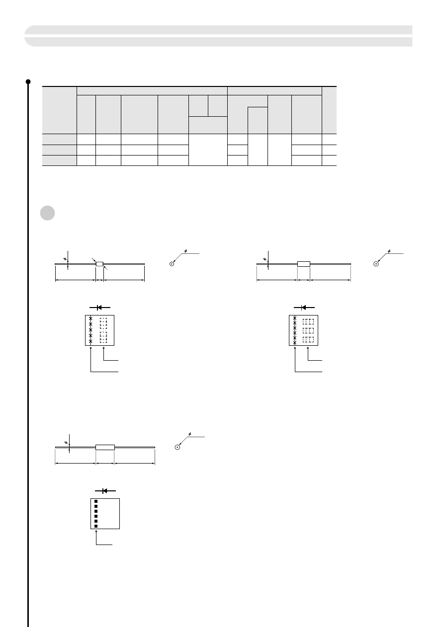
Absolute Maximum Ratings
Electrical Characteristics (Ta=25ºC)
V
RM
(kV)
I
F (AV)
(mA)
50 Hz
half-wave
signal
average
I
RSM
(mA)
Peak value of
single shot
triangular wave
with 100
µ
s
half-power
bandwidth
I
RSM
(A)
Peak value
of 50 Hz
half-wave
signal
V
F
(V)
max
V
z
(kV)
I
R
=100
µ
A
I
R
(
µ
A)
V
R
=V
RM
max
Condition
I
F
(mA)
Fig.
No.
T
j
T
stg
(ºC)
SHV-05JS
SHV-08J
SHV-30J
2.5
4.0
15.0
30
30
30
30
30
10
3
3
–40 to +150
3
5
8
10
10
30
2.6 to 5.0
4.5 to 8.0
16.0 to 30.0
1
2
3
27min
5
±
0.2
0.5
C0.5
C0.5
2.5
±
0.2
27min
Lot No.
Part No. code and cathode marking
27min
12
±
0.2
0.6
3.0
±
0.2
27min
Part No. code and cathode marking (white)
27min
8
±
0.2
0.6
3.0
±
0.2
27min
Lot No.
Part No. code and cathode marking (white)
Part No.
High-voltage Diodes for Igniters
108
External Dimensions
(unit: mm)
Fig. 1 (SHV-05JS)
Fig. 3 (SHV-30J)
Fig. 2 (SHV-08J)
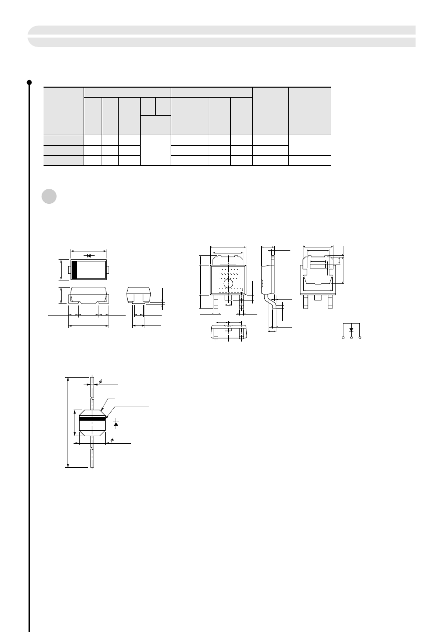
109
–40 to +150
Absolute Maximum Ratings
Electrical Characteristics
P
R
(W)
V
DC
(V)
I
ZSM
(A)
10ms
rectangular
wave
single shot
Tstg
Tj
V
Z
(V)
1mA
instantaneous
current
Part No.
Remarks
Surface-mount
type
External
dimensions
(ºC)
I
R (H)
(mA)
max
I
R
(
µ
A)
max
SFPZ-68
50
1500
PZ 628
20
20
2
65
28
±
3.0
28
±
3.0
10
1.0
500
1.0
1
3
450
SPZ-G36
30
11
36
±
3.6
5
0.1
2
(Ta=25ºC)
Power Zener Diode
Fig. 1
Fig. 3
Fig. 2
External Dimensions
(unit: mm)
56.0
1.3
±
0.05
±
0.2
±
0.7
±
0.02
10.0
C2
10.0
Cathode marking
6.5
±
0.4
2.3
±
0.4
5.4
4.9
4.1
5.4
a
b
c
±
0.4
1.7
±
0.5
5.5
±
0.4
2.5
±
0.4
0.8
±
0.1
0.8
1.5 max
±
0.1
0.55
±
0.1
0.55
±
0.1
1.15
±
0.1
1.2max
2.29
±
0.5
2.29
±
0.5
0 to 0.25
0.5
±
0.2
2.9
0.16
1.
3
7
5.0
0.7
a) Part No.
b) Polarity
c) Lot No.
4.5
±
0.2
±
0.2
±
0.2
±
0.2
±
0.4
±
0.4
±
0.2
0.05
2.0min
1.35
1.35
5.1
+0.4
–0.1
2.6
2.05
1.1
1.5
Absolute Maximum Ratings
Electrical Characteristics
V
RM
(V)
I
F (AV)
(A)
I
FSM
(A)
V
F
(V)
max
Tstg
Tj
I
R
(
µ
A)
max
Part No.
(ºC)
Condition
I
F
(A)
SFPM-52
SFPM-62
SFPM-54
SFPM-64
200
400
0.9
1.0
0.9
1.0
30
45
30
45
1.0
0.98
1.0
0.98
1.0
1.0
1.0
1.0
10
10
10
10
–40 to +150
–40 to +150
–40 to +150
–40 to +150
1
1
■
Surface-mount Type
Absolute Maximum Ratings
Electrical Characteristics
V
RM
(V)
I
F (AV)
(A)
I
FSM
(A)
V
F
(V)
max
Tstg
Tj
I
R
(
µ
A)
max
Part No.
(ºC)
Condition
I
F
(A)
RM 1C
EM 1C
RO 2C
RM 11C
RM 2C
RM 3C
RM 4C
0.8
1.0
1.2
2.0
3.0
1000
40
35
80
100
150
150
1.2
0.97
0.92
0.92
0.91
0.95
0.95
1.0
1.0
1.5
1.5
1.5
2.5
3.0
5
20
10
10
10
10
10
5
4
6
5
6
7
8
–40 to +150
–40 to +150
–40 to +150
–40 to +150
–40 to +150
–40 to +150
–40 to +150
Absolute Maximum Ratings
Electrical Characteristics
V
RM
(V)
I
F (AV)
(A)
I
FSM
(A)
V
F
(V)
max
Tstg
Tj
I
R
(
µ
A)
max
Part No.
(ºC)
Condition
I
F
(A)
FMM-31S,R
FMM-22S,R
FMM-32S,R
FMM-24S,R
FMM-34S,R
FMM-26S,R
FMM-36S,R
20
10
20
10
20
10
20
100
200
400
600
120
100
120
100
120
100
120
1.10
1.10
1.10
1.10
1.10
1.10
1.10
10
5.0
10
5.0
10
5.0
10
10
10
10
10
10
10
10
10
9
10
9
10
9
10
–40 to +150
–40 to +150
–40 to +150
–40 to +150
–40 to +150
–40 to +150
–40 to +150
Absolute Maximum Ratings
Electrical Characteristics
V
RM
(V)
I
F (AV)
(A)
I
FSM
(A)
V
F
(V)
max
Tstg
Tj
I
R
(
µ
A)
max
Part No.
(ºC)
Condition
I
F
(A)
100
200
400
600
800
1.0
3.0
1.0
1.2
1.5
3.0
1.0
1.2
2.5
3.0
1.0
1.2
2.5
3.0
3.2
0.8
1.0
1.2
2.0
3.0
45
200
35
45
50
80
100
120
200
35
45
50
80
100
150
150
200
35
45
50
80
100
150
150
200
350
40
35
80
100
150
150
150
0.97
0.95
0.98
0.97
0.97
0.95
0.92
0.91
0.91
0.95
0.98
0.97
0.97
0.95
0.92
0.92
0.91
0.91
0.95
0.95
0.98
0.97
0.97
0.95
0.92
0.92
0.92
0.91
0.91
0.95
0.95
0.92
1.2
0.97
0.92
0.92
0.92
0.91
0.91
0.95
0.95
1.0
3.0
1.0
1.0
1.0
1.0
1.5
1.5
1.5
3.0
1.0
1.0
1.0
1.0
1.2
1.5
1.5
1.5
2.5
3.0
1.0
1.0
1.0
1.0
1.2
1.5
1.5
1.5
1.5
2.5
3.0
3.5
1.0
1.0
1.2
1.5
1.5
1.5
1.5
2.5
3.0
10
10
10
10
10
5
10
10
10
10
10
10
10
5
10
10
10
10
10
10
10
10
10
5
10
10
10
10
10
10
10
10
5
20
10
10
10
10
10
10
10
4
8
2
3
4
5
6
5
8
2
3
4
5
4
6
5
7
8
2
3
4
5
4
6
5
6
5
7
8
5
4
6
5
6
5
7
8
–40 to +150
–40 to +150
–40 to +150
–40 to +150
–40 to +150
–40 to +150
–40 to +150
–40 to +150
–40 to +150
–40 to +150
–40 to +150
–40 to +150
–40 to +150
–40 to +150
–40 to +150
–40 to +150
–40 to +150
–40 to +150
–40 to +150
–40 to +150
–40 to +150
–40 to +150
–40 to +150
–40 to +150
–40 to +150
–40 to +150
–40 to +150
–40 to +150
–40 to +150
–40 to +150
–40 to +150
–40 to +150
–40 to +150
–40 to +150
–40 to +150
–40 to +150
–40 to +150
–40 to +150
–40 to +150
–40 to +150
–40 to +150
■
Axial Type
■
Center-tap Type
Rectifier Diodes
110
General-purpose Diodes
EM 1Y
RM 4Y
AM01Z
EM01Z
EM 1Z
RM 1Z
RO 2Z
RM 2Z
RM 10Z
RM 4Z
AM01
EM01
EM 1
RM 1
EM 2
RO 2
RM 2
RM 10
RM 3
RM 4
AM01A
EM01A
EM 1A
RM 1A
EM 2A
RO 2A
RM 11A
RM 2A
RM 10A
RM 3A
RM 4A
RM 4AM
RM 1B
EM 1B
EM 2B
RO 2B
RM 11B
RM 2B
RM 10B
RM 3B
RM 4B
Fig.
No.
Fig.
No.
Fig.
No.
Fig.
No.
■
Axial Type
■
Frame 2-pin Type
■
Center-tap Type
111
Fast Recovery Rectifier Diodes
100
200
400
600
Absolute Maximum Ratings
Electrical Characteristics
V
RM
(V)
I
F (AV)
(A)
I
FSM
(A)
Tstg
Tj
V
F
(V)
max
Part No.
(ºC)
I
R
(
µ
A)
max
trr1
(
µ
s)
max
trr2
(
µ
s)
max
EU 2YX
RU 2YX
RU 3YX
RU 4Y
RU 30Y
RU 4YX
EU01Z
EU 1Z
AU01Z
RF 1Z
AS01Z
EH 1Z
RH 1Z
ES01Z
ES 1Z
AU02Z
EU02Z
EU 2Z
RU 2Z
RU 4Z
RU 30Z
RU 1
EU01
EU 1
AU01
RF 1
AS01
EH 1
RH 1
ES01
ES 1
AU02
EU02
EU 2
RU 2M
RU 3
RU 3M
RU 30
RU 4
RU 31
RU 4M
RU 1A
EU01A
EU 1A
RF 1A
AS01A
EH 1A
RH 1A
ES01A
ES 1A
RS 1A
1.2
1.5
2.0
3.5
4.0
0.25
0.5
0.6
0.7
0.8
1.0
3.5
0.25
0.5
0.6
0.7
0.8
1.0
1.1
1.5
2.0
3.0
3.5
0.25
0.6
0.7
25
30
50
70
80
70
15
15
15
20
30
35
30
25
15
20
70
80
15
15
15
20
30
35
30
25
15
15
20
20
50
200
50
150
70
15
15
20
30
35
30
0.9
0.95
0.95
1.3
0.97
1.3
2.5
2.5
1.7
2.0
1.5
1.35
1.3
2.5
2.5
1.3
1.4
1.4
1.5
1.3
0.97
2.5
2.5
2.5
1.7
2.0
1.5
1.35
1.3
2.5
2.5
1.3
1.4
1.4
1.2
1.5
1.1
0.95
1.5
1.2
1.3
2.5
2.5
2.5
2.0
1.5
1.35
1.3
2.5
2.5
2.5
0.2
0.2
0.2
0.4
0.4
0.4
0.4
0.4
0.4
0.4
1.5
4.0
4.0
1.5
1.5
0.4
0.4
0.4
0.4
0.4
0.4
0.4
0.4
0.4
0.4
0.4
1.5
4.0
4.0
1.5
1.5
0.4
0.4
0.4
0.4
0.4
0.4
0.4
0.4
0.4
0.4
0.4
0.4
0.4
0.4
1.5
4.0
4.0
1.5
1.5
1.5
10
10
10
10
10
10
10
10
10
10
10
10
5
10
10
10
10
10
10
10
10
10
10
10
10
10
10
10
5
10
10
10
10
10
10
10
10
10
10
50
10
10
10
10
10
10
10
5
10
10
10
0.08
0.08
0.08
0.18
0.18
0.18
0.18
0.18
0.18
0.18
0.6
1.3
1.3
0.6
0.6
0.18
0.18
0.18
0.18
0.18
0.18
0.18
0.18
0.18
0.18
0.18
0.6
1.3
1.3
0.6
0.6
0.18
0.18
0.18
0.18
0.18
0.18
0.18
0.18
0.18
0.18
0.18
0.18
0.18
0.18
0.6
1.3
1.3
0.6
0.6
0.6
4
5
6
8
7
8
3
4
2
5
2
4
5
3
4
2
3
4
5
8
7
5
3
4
2
5
2
4
5
4
2
3
4
5
6
7
8
7
8
5
3
4
5
2
4
5
3
4
5
–40 to +150
–40 to +150
–40 to +150
–40 to +150
–40 to +150
–40 to +150
–40 to +150
–40 to +150
–40 to +150
–40 to +150
–40 to +150
–40 to +150
–40 to +150
–40 to +150
–40 to +150
–40 to +150
–40 to +150
–40 to +150
–40 to +150
–40 to +150
–40 to +150
–40 to +150
–40 to +150
–40 to +150
–40 to +150
–40 to +150
–40 to +150
–40 to +150
–40 to +150
–40 to +150
–40 to +150
–40 to +150
–40 to +150
–40 to +150
–40 to +150
–40 to +150
–40 to +150
–40 to +150
–40 to +150
–40 to +150
–40 to +150
–40 to +150
–40 to +150
–40 to +150
–40 to +150
–40 to +150
–40 to +150
–40 to +150
–40 to +150
–40 to +150
–40 to +150
100
200
400
Absolute Maximum Ratings
Electrical Characteristics
V
RM
(V)
I
F (AV)
(A)
I
FSM
(A)
Tstg
Tj
V
F
(V)
max
Part No.
(ºC)
I
R
(
µ
A)
max
trr1
(
µ
s)
max
trr2
(
µ
s)
max
FMU-21S,R
FMU-12S,R
FMU-22S,R
FMU-32S,R
FMU-14S,R
FMU-24S,R
FMU-34S,R
10.0
5.0
10.0
20.0
5.0
10.0
20.0
40
30
40
80
30
40
80
1.5
1.5
1.5
1.5
1.5
1.5
1.5
0.4
0.4
0.4
0.4
0.4
0.4
0.4
50
50
50
50
50
50
50
0.18
0.18
0.18
0.18
0.18
0.18
0.18
9
9
10
9
10
–40 to +150
–40 to +150
–40 to +150
–40 to +150
–40 to +150
–40 to +150
–40 to +150
100
Absolute Maximum Ratings
Electrical Characteristics
V
RM
(V)
I
F (AV)
(A)
I
FSM
(A)
Tstg
Tj
V
F
(V)
max
Part No.
(ºC)
I
R
(
µ
A)
max
trr1
(
µ
s)
max
trr2
(
µ
s)
max
FMU-G2YXS
10.0
100
1.0
0.2
50
0.08
11
–40 to +150
600
800
1000
1500
2000
Absolute Maximum Ratings
Electrical Characteristics
V
RM
(V)
I
F (AV)
(A)
I
FSM
(A)
Tstg
Tj
V
F
(V)
max
Part No.
(ºC)
I
R
(
µ
A)
max
trr1
(
µ
s)
max
trr2
(
µ
s)
max
EU02A
EU 2A
RU 2
RU 2AM
RU 3A
RU 20A
RU 3AM
RU 30A
RU 4A
RU 31A
RU 4AM
RU 1B
RF 1B
RH 1B
RS 1B
RU 2B
RU 3B
RU 4B
RU 1C
RH 1C
RU 2C
RU 3C
RU 4C
ES01F
ES 1F
RC 2
1.0
1.1
1.5
2.0
3.0
3.5
0.25
0.6
0.7
1.0
1.1
3.0
0.2
0.6
0.8
1.5
2.5
0.5
0.2
15
20
20
20
50
200
50
150
70
15
15
35
30
20
20
50
15
35
20
20
50
20
20
1.4
1.4
1.5
1.2
1.5
1.1
1.1
0.95
1.5
1.2
1.3
2.5
2.0
1.3
2.5
1.5
1.5
1.6
3.0
1.3
1.5
2.5
1.6
2.0
2.0
2.0
0.4
0.4
0.4
0.4
0.4
0.4
0.4
0.4
0.4
0.4
0.4
0.4
0.4
4.0
1.5
0.4
0.4
0.4
0.4
4.0
0.4
0.4
0.4
1.5
1.5
4.0
10
10
10
10
10
10
10
10
10
50
10
10
10
5
10
10
10
10
10
5
10
10
50
10
10
10
0.18
0.18
0.18
0.18
0.18
0.18
0.18
0.18
0.18
0.18
0.18
0.18
0.18
1.3
0.6
0.18
0.18
0.18
0.18
1.3
0.18
0.18
0.18
0.6
0.6
1.3
3
4
5
6
5
6
7
8
7
8
5
6
8
5
6
8
3
4
5
–40 to +150
–40 to +150
–40 to +150
–40 to +150
–40 to +150
–40 to +150
–40 to +150
–40 to +150
–40 to +150
–40 to +150
–40 to +150
–40 to +150
–40 to +150
–40 to +150
–40 to +150
–40 to +150
–40 to +150
–40 to +150
–40 to +150
–40 to +150
–40 to +150
–40 to +150
–40 to +150
–40 to +150
–40 to +150
–40 to +150
General-purpose Diodes
Fig.
No.
Fig.
No.
Fig.
No.
Fig.
No.
●
trr1=I
F
/I
RP
=1: 1, trr2=I
F
/I
RP
=1: 2
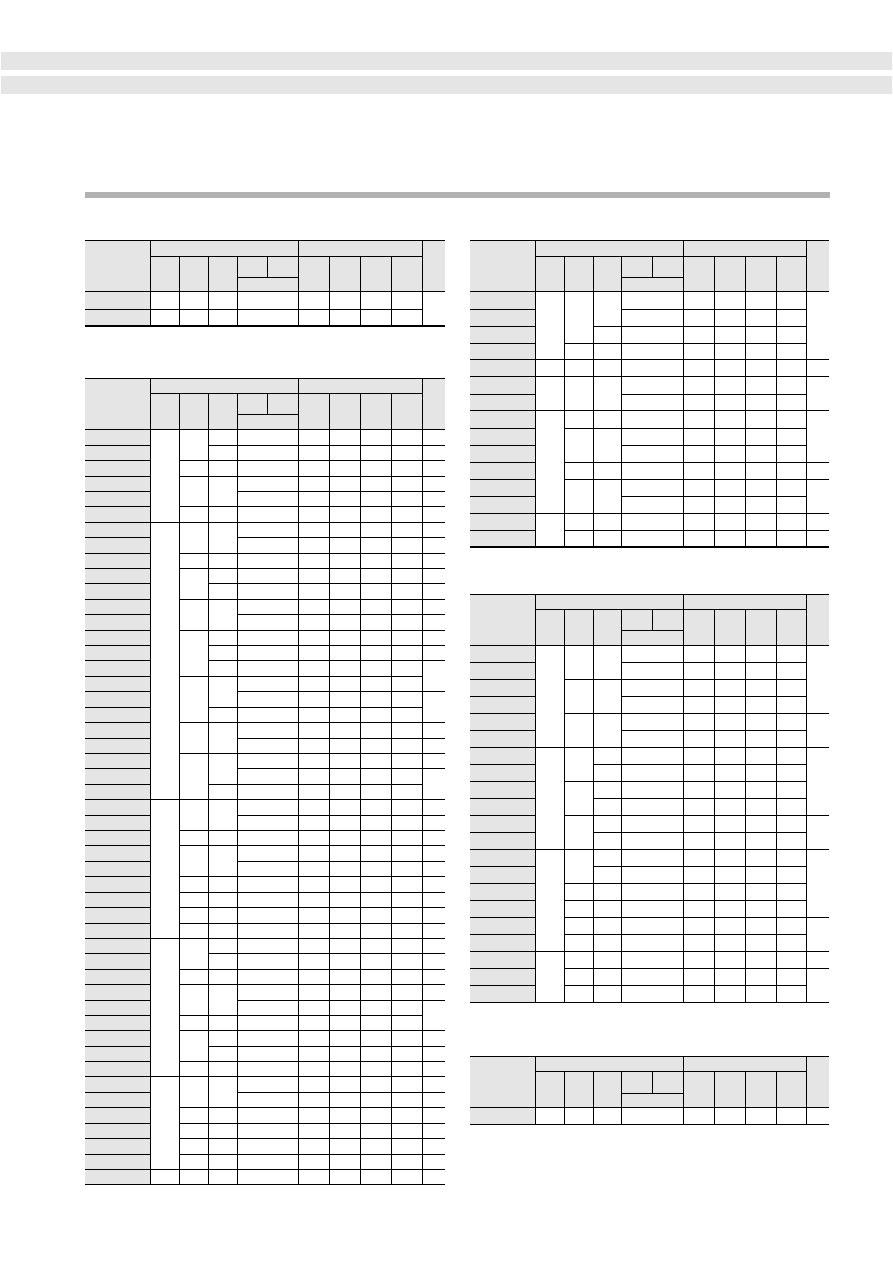
Ultra Fast Recovery Rectifier Diodes
112
Absolute Maximum Ratings
Electrical Characteristics
V
RM
(V)
I
F (AV)
(A)
I
FSM
(A)
Tstg
Tj
V
F
(V)
max
Part No.
(ºC)
I
R
(
µ
A)
max
trr1
(ns)
max
trr2
(ns)
max
Absolute Maximum Ratings
Electrical Characteristics
V
RM
(V)
I
F (AV)
(A)
I
FSM
(A)
Tstg
Tj
V
F
(V)
max
Part No.
(ºC)
I
R
(
µ
A)
max
trr1
(
µ
s)
max
trr2
(
µ
s)
max
■
Axial Type
■
Center-tap Type
■
Bridge Type
SFPL-52
SFPL-62
200
200
0.9
1.0
25
25
0.98
0.98
10
10
50
50
35
35
1
–40 to +150
–40 to +150
Absolute Maximum Ratings
Electrical Characteristics
V
RM
(V)
I
F (AV)
(A)
I
FSM
(A)
Tstg
Tj
V
F
(V)
max
Part No.
(ºC)
I
R
(
µ
A)
max
trr1
(ns)
max
trr2
(ns)
max
FMP-G12S
FML-G12S
FMN-G12S
FML-G22S
FML-G13S
FMN-G14S
FML-G14S
FMG-G26S
FMN-G16S
FML-G16S
FMG-G36S
FML-G26S
FMD-G26S
FMG-G2CS
FMG-G3CS
200
300
400
600
1000
200
300
400
600
5.0
10.0
5.0
5.0
4.0
5.0
8.0
10.0
4.0
5.0
65
100
150
70
70
50
50
80
100
30
60
1.15
0.98
0.92
0.98
1.3
1.0
1.3
2.5
1.2
1.5
2.5
1.7
1.7
4.0
3.5
50
250
100
500
100
50
100
500
50
100
500
100
100
50
100
150
40
100
40
50
100
50
100
100
50
100
65
50
100
150
70
30
50
30
35
50
35
50
50
35
50
40
30
50
70
11
11
11
11
12
11
11
12
–40 to +150
–40 to +150
–40 to +150
–40 to +150
–40 to +150
–40 to +150
–40 to +150
–40 to +150
–40 to +150
–40 to +150
–40 to +150
–40 to +150
–40 to +150
–40 to +150
–40 to +150
Absolute Maximum Ratings
Electrical Characteristics
V
RM
(V)
I
F (AV)
(A)
I
FSM
(A)
Tstg
Tj
V
F
(V)
max
Part No.
(ºC)
I
R
(
µ
A)
max
trr1
(ns)
max
trr2
(ns)
max
FMG-12S,R
FML-12S
FMG-22S,R
FML-22S
FMG-32S,R
FML-32S
FMG-13S,R
FML-13S
FMG-23S,R
FML-23S
FML-33S
FMG-33S,R
FMG-14S,R
FML-14S
FMG-24S,R
FML-24S
FMG-34S,R
FML-34S
FMG-26S,R
FMG-36S,R
FML-36S
5.0
10.0
20.0
5.0
10.0
20.0
5.0
8.0
10.0
16.0
20.0
6.0
15.0
20.0
35
65
150
35
40
65
70
100
150
35
40
65
70
100
100
50
80
100
1.8
0.98
1.8
0.98
1.8
0.98
1.8
1.3
1.8
1.3
1.3
1.8
2.0
1.3
2.0
1.3
2.0
1.3
2.2
2.2
1.7
500
150
500
250
1000
600
500
50
500
100
200
1000
500
50
500
100
1000
200
500
1000
100
100
40
100
40
100
40
100
50
100
50
50
100
100
50
100
50
100
50
100
100
65
50
30
50
30
50
30
50
35
50
35
35
50
50
35
50
35
50
35
50
50
35
9
10
9
10
9
10
9
10
–40 to +150
–40 to +150
–40 to +150
–40 to +150
–40 to +150
–40 to +150
–40 to +150
–40 to +150
–40 to +150
–40 to +150
–40 to +150
–40 to +150
–40 to +150
–40 to +150
–40 to +150
–40 to +150
–40 to +150
–40 to +150
–40 to +150
–40 to +150
–40 to +150
200
Absolute Maximum Ratings
Electrical Characteristics
V
RM
(V)
I
F (AV)
(A)
I
FSM
(A)
Tstg
Tj
V
F
(V)
max
Part No.
(ºC)
I
R
(
µ
A)
max
trr1
(ns)
max
trr2
(ns)
max
RBV-602L
6
100
1
250
50
35
13
–40 to +150
AG01Y
EG01Y
EG 1Y
RG 10Y
RG 2Y
RG 4Y
AG01Z
EG01Z
EG 1Z
AL01Z
EN 01Z
RG 10Z
RG 2Z
EL 1Z
EL02Z
RN 1Z
RL 10Z
RL 2Z
RN 2Z
RN 3Z
RG 4Z
RL 3Z
RL 4Z
RN 4Z
AG01
EG01
EG 1
RG 10
RG 2
EL 1
RL 2
RG 4
RL 3
EG01A
AG01A
EG 1A
RG 10A
RG 2A
RL 2A
RG 4A
RL 3A
RL 4A
AP01C
EP01C
RU 1P
EG01C
RG 1C
RG 4C
RP 1H
70
200
400
600
1000
2000
1.0
1.1
1.5
3.5
0.7
0.8
1.0
1.2
1.5
2.0
3.0
3.5
0.7
0.8
1.2
1.5
2.0
3.0
3.5
0.5
0.6
1.0
1.2
2.0
3.0
0.2
0.4
0.5
0.7
2.0
0.1
25
30
30
50
100
15
15
25
50
50
20
25
60
30
70
80
80
120
15
15
50
20
40
80
80
10
15
10
50
30
50
60
80
5
10
10
10
60
5
1.2
1.2
1.2
1.1
1.1
1.3
1.8
1.9
1.7
0.98
0.92
1.5
1.5
0.98
0.98
0.92
0.98
0.98
0.92
0.92
1.7
0.95
0.95
0.92
1.8
2.0
1.8
1.8
1.8
1.3
1.3
1.8
1.3
2.0
1.8
2.0
2.0
2.0
1.55
2.0
1.7
1.5
4.0
4.0
4.0
3.3
3.3
3.0
7.0
100
100
100
500
500
1000
100
50
50
100
10
500
500
100
50
20
50
100
50
50
1000
50
150
50
100
50
50
500
500
10
10
500
100
100
100
100
500
500
50
500
50
50
100
5
5
50
20
500
20
100
100
100
100
100
100
100
100
100
50
100
100
100
100
40
100
50
50
100
100
100
50
50
100
100
100
100
100
100
100
50
100
50
100
100
100
100
100
50
100
50
50
200
200
100
100
100
100
200
50
50
50
50
50
50
50
50
50
35
50
50
50
50
30
50
35
35
50
50
50
35
35
50
50
50
50
50
50
50
35
50
35
50
50
50
50
50
35
50
35
35
80
80
50
50
50
50
80
2
3
4
5
6
8
2
3
4
2
3
5
6
4
3
5
6
7
8
7
8
2
3
4
5
6
4
6
8
7
3
2
4
5
6
8
7
8
2
3
5
3
5
8
5
–40 to +150
–40 to +150
–40 to +150
–40 to +150
–40 to +150
–40 to +150
–40 to +150
–40 to +150
–40 to +150
–40 to +150
–40 to +150
–40 to +150
–40 to +150
–40 to +150
–40 to +150
–40 to +150
–40 to +150
–40 to +150
–40 to +150
–40 to +150
–40 to +150
–40 to +150
–40 to +150
–40 to +150
–40 to +150
–40 to +150
–40 to +150
–40 to +150
–40 to +150
–40 to +150
–40 to +150
–40 to +150
–40 to +150
–40 to +150
–40 to +150
–40 to +150
–40 to +150
–40 to +150
–40 to +150
–40 to +150
–40 to +150
–40 to +150
–40 to +150
–40 to +150
–40 to +150
–40 to +150
–40 to +150
–40 to +150
–40 to +150
■
Surface-mount Type
■
Frame 2-pin Type
General-purpose Diodes
●
trr1=I
F
/I
RP
=1: 1, trr2=I
F
/I
RP
=1: 2
Fig.
No.
Fig.
No.
Fig.
No.
Fig.
No.
Fig.
No.
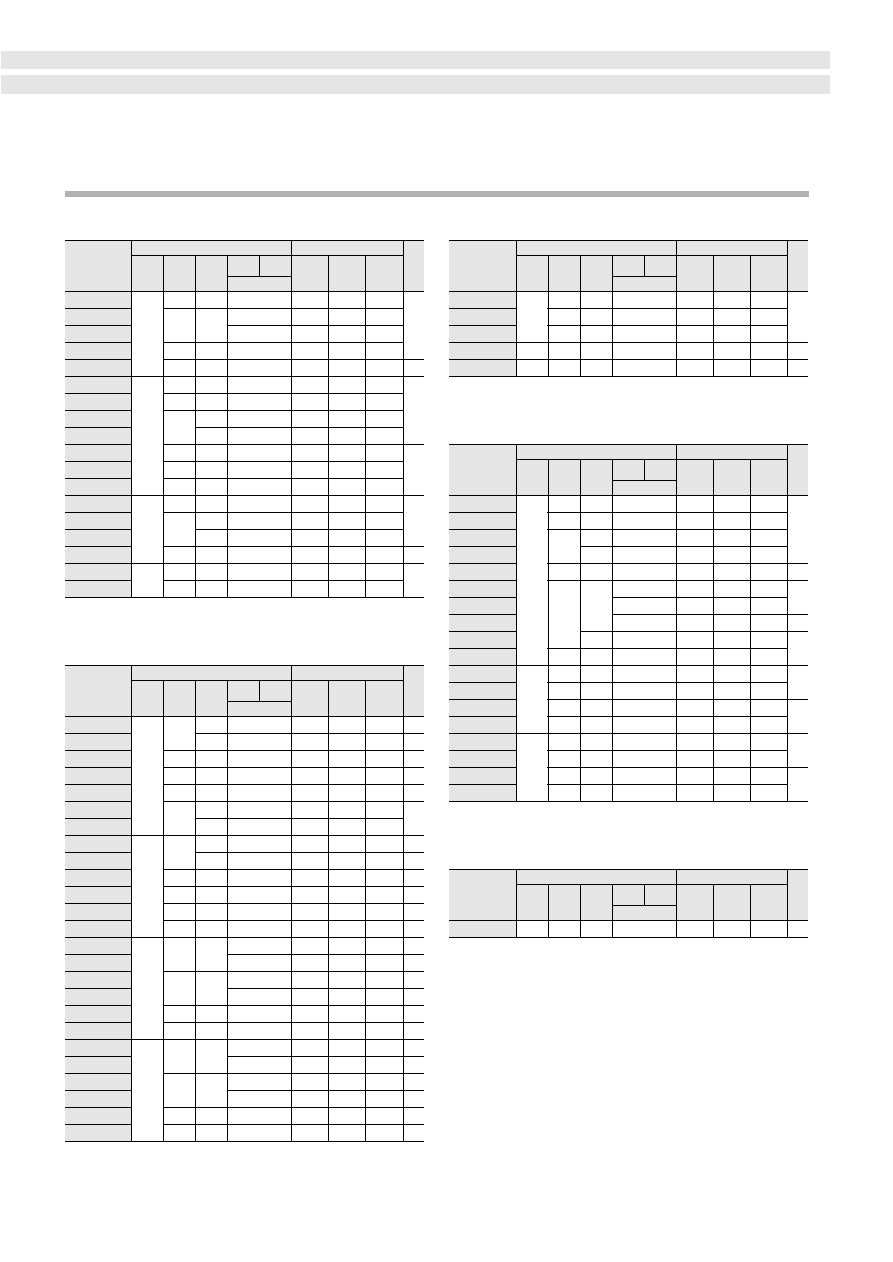
113
Schottky Barrier Diodes
■
Surface-mount Type
■
Axial Type
■
Bridge Type
Absolute Maximum Ratings
Electrical Characteristics
V
RM
(V)
I
F (AV)
(A)
I
FSM
(A)
Tstg
Tj
Part No.
(ºC)
H•I
R
(mA)
Ta=100ºC
max
FMB-G14
FMB-G14L
FMB-G24H
FMB-G16L
FMB-G19L
40
60
90
60
60
150
50
60
3.0
5.0
10.0
6.0
4.0
–40 to +150
–40 to +150
–40 to +150
–40 to +150
–40 to +150
5
5
10
5
5
100
100
65
50
35
0.55
0.55
0.55
0.62
0.81
11
11
11
■
Frame 2-pin Type
■
Center-tap Type
Absolute Maximum Ratings
Electrical Characteristics
V
RM
(V)
I
F (AV)
(A)
I
FSM
(A)
Tstg
Tj
Part No.
(ºC)
H•I
R
(mA)
Ta=100ºC
max
SFPJ-53
SFPE-63
SFPJ-63
SFPJ-73
SPJ-63S
SFPB-54
SFPB-64
SFPE-64
SFPB-74
SPB-G34S
SPB-G54S
SPB-64S
SFPB-56
SFPB-66
SFPB-76
SPB-G56S
SFPB-59
SFPB-69
30
40
60
90
30
40
50
50
30
60
40
60
50
60
50
10
25
40
60
10
40
1.0
2.0
3.0
6.0
1.0
1.5
2.0
3.0
5.0
6.0
0.7
2.0
5.0
0.7
1.5
–40 to +150
–40 to +150
–40 to +150
–40 to +150
–40 to +150
–40 to +150
–40 to +150
–40 to +150
–40 to +150
–40 to +150
–40 to +150
–40 to +150
–40 to +150
–40 to +150
–40 to +150
–40 to +150
–40 to +150
–40 to +150
1.0
0.2
2.0
3.0
3
1
5
0.2
5
3.5
5
3.5
1
1
2
3
1
2
10
20
30
50
50
50
50
50
50
7.5
15
20
50
5
10
0.45
0.55
0.45
0.45
0.45
0.55
0.55
0.6
0.5
0.55
0.55
0.55
0.62
0.69
0.62
0.7
0.81
0.81
1
14
1
14
1
14
1
Absolute Maximum Ratings
Electrical Characteristics
V
RM
(V)
I
F (AV)
(A)
I
FSM
(A)
Tstg
Tj
Part No.
(ºC)
H•I
R
(mA)
Ta=100ºC
max
FMB-24
FMB-24M
FMB-24L
FME-24L
FMB-34S
FMB-24H
FME-24H
MPE-24H
FMB-34
FMB-34M
FMB-26
FMB-26L
FMB-36
FMB-36M
FMB-29
FMB-29L
FMB-39
FMB-39M
40
60
90
50
60
60
80
75
100
150
300
40
50
100
150
50
60
60
150
4.0
6.0
10
12
15
30
4.0
10
15
30
4.0
8.0
15
20
–40 to +150
–40 to +150
–40 to +150
–40 to +150
–40 to +150
–40 to +150
–40 to +150
–40 to +150
–40 to +150
–40 to +150
–40 to +150
–40 to +150
–40 to +150
–40 to +150
–40 to +150
–40 to +150
–40 to +150
–40 to +150
5
5
5
0.5
5
7.5
0.75
0.75
10
20
1
2.5
5
10
3
5
10
15
0.55
0.55
0.55
0.6
0.58
0.55
0.6
0.6
0.55
0.55
0.62
0.62
0.62
0.62
0.81
0.81
0.81
0.81
9
10
9
15
10
9
10
9
10
35
35
35
30
35
50
50
65
100
20
50
75
150
15
35
50
60
Absolute Maximum Ratings
Electrical Characteristics
V
RM
(V)
I
F (AV)
(A)
I
FSM
(A)
Tstg
Tj
Part No.
(ºC)
H•I
R
(mA)
Ta=100ºC
max
RBV-406B
60
40
4.0
–40 to +150
2
0.62
13
20
50
(Tj=150ºC)
20
(Tj=150ºC)
30
(Tj=125ºC)
20
(Tj=150ºC)
Absolute Maximum Ratings
Electrical Characteristics
V
RM
(V)
I
F (AV)
(A)
I
FSM
(A)
Tstg
Tj
V
F
(V)
max
Part No.
(ºC)
I
R
(mA)
max
H•I
R
(mA)
Ta=100ºC
max
AK 03
EK 03
EK 13
RK 13
RK 33
RJ 43
RK 43
AK 04
EK 04
EK 14
RK 14
RK 34
RK 44
AK 06
EK 06
EK 16
RK 16
RK 36
RK 46
AK 09
EK 09
EK 19
RK 19
RK 39
RK 49
30
40
60
90
25
40
40
60
50
50
80
25
40
40
60
50
80
10
25
40
70
10
40
50
60
1.0
1.5
1.7
2.5
3.0
1.0
1.5
1.7
2.5
3.0
0.7
1.5
2.0
3.5
0.7
1.5
2.0
3.5
–40 to +150
–40 to +150
–40 to +150
–40 to +150
–40 to +150
–40 to +150
–40 to +150
–40 to +150
–40 to +150
–40 to +150
–40 to +150
–40 to +150
–40 to +150
–40 to +150
–40 to +150
–40 to +150
–40 to +150
–40 to +150
–40 to +150
–40 to +150
–40 to +150
–40 to +150
–40 to +150
–40 to +150
–40 to +150
1
5
5
5
5
3
5
1
5
5
5
5
5
1
1
1
1
2
3
1
1
2
2
3
5
50
50
50
50
30
50
50
50
50
50
50
7.5
7.5
15
15
20
35
5
5
10
10
15
35
0.55
0.55
0.55
0.55
0.55
0.45
0.55
0.55
0.55
0.55
0.55
0.55
0.55
0.62
0.62
0.62
0.62
0.62
0.62
0.81
0.81
0.81
0.81
0.81
0.81
2
3
4
5
6
8
2
3
4
5
6
8
2
3
4
5
6
8
2
3
4
5
6
8
50
(Tj=100ºC)
50
(Tj=100ºC)
V
F
(V)
max
I
R
(mA)
max
V
F
(V)
max
I
R
(mA)
max
V
F
(V)
max
I
R
(mA)
max
V
F
(V)
max
I
R
(mA)
max
General-purpose Diodes
Fig.
No.
Fig.
No.
Fig.
No.
Fig.
No.
Fig.
No.
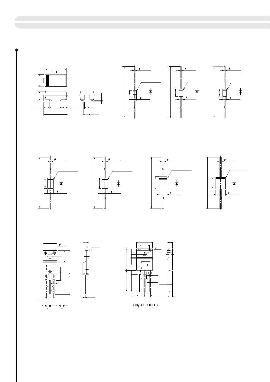
4.5
±
0.2
0.05
2.0min
1.35
±
0.4
1.35
±
0.4
5.1
+0.4
–0.1
2.6
±
0.2
2.05
±
0.2
1.1
±
0.2
1.5
±
0.2
50.0
±
1.0
2.9
±
0.1
2.4
±
0.1
0.57
±
0.02
Cathode marking
62.3
±
0.7
5.0
±
0.2
2.7
±
0.2
0.78
±
0.05
Cathode marking
62.5
±
0.7
7.2
±
0.2
4.0
±
0.2
0.78
±
0.05
Cathode marking
62.5
±
0.7
7.2
±
0.2
4.0
±
0.2
0.98
±
0.05
Cathode marking
50.0
±
0.1
1.4
±
0.1
6.5
±
0.2
Cathode marking
8.0
±
0.2
62.5
±
0.7
1.2
±
0.05
5.2
±
0.2
Cathode marking
9.1
±
0.2
9.0
15.0
5.0
2.8
3.5
16.5
20.0
20.0
0.8
3.3
3.4
2.3
1.0
5.45
5.45
5.0
0.65
2.6
–0.1
+0.2
±
0.5
±
0.5
S type
(SBD)
R type
S type
(SBD)
R type
a
b
a
b
c
0.6
±
0.05
2.7
±
0.2
5.0
±
0.2
62.3
±
0.7
Cathode marking
General-purpose Diodes - External Dimensions
114
Fig. 1
Fig. 2
Fig. 3
Fig. 4
Fig. 5
Fig. 6
Fig. 9
Fig. 10
Fig. 7
Fig. 8
a) Part No.
b) Lot No.
a) Part No.
b) Polarity
c) Lot No.
C 0.5
16.9
(13.5)
8.4
0.8
3.9
4
10.0
2.6
4.2
2.8
1.35
1.35
0.85
2.54
2.54
0.45
3.3
(Unit: mm)

1.2
1.27
10.2
0.86
0.76
2.54
2.54
4.44
1.3
2.59
0.4
3.19
1.
3
8.5
10.0
11.3
11.0
1.4
115
Fig. 11 Full-mold
Fig. 14
Fig. 15
Fig. 12 Full-mold
Fig. 13
6.5
±
0.4
2.3
±
0.4
5.4
4.9
4.1
5.4
a
b
c
±
0.4
1.7
±
0.5
5.5
±
0.4
2.5
±
0.4
0.8
±
0.1
0.8
1.5 max
±
0.1
0.55
±
0.1
0.55
±
0.1
1.15
1
2
3
±
0.1
1.2max
2.29
±
0.5
2.29
±
0.5
0 to 0.25
0.5
±
0.2
2.9
0.16
1
.37
5.0
0.7
a) Part No.
b) Polarity
c) Lot No.
9.0
15.0
5.0
2.8
3.5
16.5
20.0
20.0
0.8
3.3
3.4
2.3
1.0
5.45
5.45
5.0
0.65
2.6
–0.1
+0.2
±
0.5
±
0.2
a) Part No.
b) Polarity
c) Lot No.
a
b
c
General-purpose Diodes - External Dimensions
16.9
(13.5)
8.4
0.8
3.9
4.0
10.0
2.2
2.6
4.2
2.8
1.35
0.85
5.08
0.45
3.3
10
7.5 7.5
30
11
13
4-1.0
4.6
3.6
2.7
20.0
17.5
C3
0.7
3.2
±
0.1
–
+
a) Part No.
b) Lot No.
a
b
(Unit: mm)

Taping
Name
Taping Dimensions (mm)
Packaging Dimensions (mm) and Markings
Packaging
Quantity
A suffix "V" is
added to Part
No. for tape
packaging.
A suffix "V" is
added to Part
No. for tape
packaging.
V
V
Emboss taping
Reel
Axial taping
Reel
(1) The cathode is on the right-hand side when viewed in the pull out direction.
(2) The electrode side of the product is on the bottom when casing.
(3) A leader tape of 150 to 200 mm in length is provided.
(4) The leading and trailing edge of the leader tape are provided with a pitch of at least 10 mm.
(5) Reversed polarity taping available on request (specify taping name "VL").
1,800 pcs.
per reel
5,000 pcs.
per reel
2.7 body
2.4 body
(4 body)
3,000 pcs.
4.5
±
0.2
0.05
2.0min
1.35
±
0.4
1.35
±
0.4
5.1
+0.4
–0.1
2.6
±
0.2
2.05
±
0.2
1.1
±
0.2
1.5
±
0.2
+0.1 –
0.05
4.0
±
0.1
2.0
3.1
2.6
12.0
±
0.3
5.5
±
0.05
1.75
±
0.1
4.0
±
0.1
5.5
Pull out direction
1.5
+0.1
–0
13
±
0.5
2.0
±
0.5
21
±
0.8
R1.0
178
±
2
14
±
1.5
2.0
±
0.5
65
Marking of Part No.,
Lot No., quantity, etc.
0.5max
1.0
–1.0
+0.5
5.08
+0.38
0.5max
max 52.0
0
+1
(Blue)
(White)
6.0
0
+5
6.0
0
+5
0.5
340
±
2
Core Flange
81
±
2
75
±
2
25
±
0.1
83
±
2
Marking of Part No.,
Lot No. and quantity
15
±
2
29
±
1
75
±
1
Stopper
A suffix "V3" is
added to Part
No. for tape
packaging.
V3
A suffix "V0" is
added to Part
No. for tape
packaging.
V0
A suffix "V1" is
added to Part
No. for tape
packaging.
V1
2,000 pcs.
per box
(2.7 body)
3000 pcs.
(2.4 body)
2,000 pcs.
per box
(2.7 body)
3000 pcs.
(2.4 body)
1000 pcs.
(4 body)
1,500 pcs.
per reel
(5.2 body)
Axial taping
Axial taping
Axial taping
Ammunition (Ammo) pack
Ammunition (Ammo) pack
Reel
0.5max
1.0
1.0
+
---
0.5
5.08
0.38
+
0.5max
max 26.0
0
+
1
(Blue)
(White)
6.0
0
+
5
6.0
0
+
5
0.5
0.5max
1.0
–1.0
+0.5
5.08
+0.38
0.5max
52.0
0
+1
(Blue)
(White)
6.0
0
+5
6.0
0
+5
max
0.5
0.5max
1.0
–1.0
+0.5
10
±
0.2
0.5max
52.0
0
+1
(Blue)
(White)
6.0
0
+5
6.0
0
+5
max
1.0
Broken lines: perforations
255max
77max
77max
Marking of Part No.,
Lot No. and quantity
Broken lines: perforations
Marking of Part No.,
Lot No. and quantity
95max
255max
51max
340
±
2
Core Flange
81
±
2
75
±
2
25
±
0.1
83
±
2
Marking of Part No.,
Lot No. and quantity
15
±
2
29
±
1
75
±
1
Stopper
Taping Specifications
General-purpose Diodes - Taping Specifications
116

Taping Specifications
Taping
Name
Taping Dimensions (mm)
Packaging Dimensions (mm) and Markings
Packaging
Quantity
A suffix "WS" is
added to Part
No. for tape
packaging.
A suffix "WK" is
added to Part
No. for tape
packaging.
WK
WS
A suffix "W" is
added to Part
No. for tape
packaging.
W
A suffix "V4" is
added to Part
No. for tape
packaging.
V4
Radial taping
2,500 pcs.
per box
(2.4 body)
1,000 pcs.
per box
(5.2 body)
4,000 pcs.
per box
2.7 body
0.6 leads only
(applies to A0 series)
Radial taping
(applies to A0 series)
Radial taping
Axial taping
Ammunition
(Ammo)
pack
Ammunition (Ammo) pack
Ammunition (Ammo) pack
0.5max
1.0
– 1.0
+0.5
10
±
0.2
0.5max
52.0
0
+1
(Blue)
(White)
6.0
0
+5
6.0
0
+5
max
1.0
4.0
±
0.2
6.35
±
1.3
12.7
±
1.0
2.6max
27.5
±
0.5
16.0
±
0.5
(11.5)
max
4.2
12.7
±
1.0
1.0
max
12.7
±
1.0
3.85
±
0.7
5.0
±
0.5
12.7
±
0.3
3.0
max
12.5
min
9.0
±
0.5
18.0
+1.0 –
0.5
0
2.0
+
---
0.7
±
0.2
3.85
±
0.7
4.0
±
0.2
5.0
+0.8
12.7
±
0.3
–0.2
0.7
±
0.2
12.5
m
in
11max
9.0
±
0.5
18.0
+1.0 –
0.5
0
±
2.0
12.7
±
1.0
6.35
±
1.3
1.0
max
18.0
+0.5 –
0
0.7
±
0.2
5.0
±
1.0
5.0
+0.8
–0
2.75
±
0.5
19.8
±
1.0
16.5
+1.0 –
0.5
11.0
4.0
±
0.3
3.0
±
0.2
12.7
±
0.3
3.85
±
0.7
12.7
±
1.0
0
±
2.0
1.5
22.2
±
1.0
9.0
±
0.5
12.5
m
in
18.0
+1.0 –
0.5
30º
Broken lines:
perforations
77max
Company
mark
Marking of Part No., Lot No. and quantity.
255max
120max
Broken lines:
perforations
Marking of Part No., Lot No. and quantity.
ANODE
CATH
ODE
340max
140max
55max
ANODE
CATH
ODE
Marking of Part No.,
Lot No. and quantity
150max
45m
ax
340max
General-purpose Diodes - Taping Specifications
117

Taping
Name
Taping Dimensions (mm)
Packaging Dimensions (mm) and Markings
Packaging
Quantity
A suffix "VR" is
added to Part
No. for tape
packaging.
VR
A suffix "VL" is
added to Part
No. for tape
packaging.
VL
3,000 pcs.
per reel
3,000 pcs.
per reel
5,000 pcs.
per reel
8,000 pcs.
per reel
Taping
Name
Taping Dimensions (mm)
Packaging Dimensions (mm) and Markings
Packaging
Quantity
A suffix "VD" is
added to Part
No. for tape
packaging.
VD
A suffix "V1" is
added to Part
No. for tape
packaging.
V1
Axial taping
Axial taping
Part No.
Quantity
Taping name
(type)
Lot No.
Materials
Disc: both-face white
corrugated cardboard
Core: foamed styrol
1.5
+0.1
–0
2.0
±
0.1
8.0
±
0.1
3.4 max
0.3
±
0.1
6.8
±
0.1
13.5
±
0.1
10.6
±
0.1
4.0
±
0.1
1.6
+0.1
–0
7.5
±
0.1
16.0
±
0.3
1.75
±
0.1
6
±
1.0
6
±
1.0
3.5
±
0.5
58
1.0 max
1.0
max
±
1
6
±
1.0
6
±
1.0
5
±
0.5
58
1.0 max
1.2
max
±
1
Part No.
Quantity
Lot No.
29
±
1.5
75
±
1.5
340
±
2
25
±
1
Pull out direction
Pull out direction
Part No.
Quantity
Lot No.
29
±
1.5
75
±
1.5
340
±
2
25
±
1
4
(6.0)
(2.0)
(40
º)
(120
º)
±
0.5
R95
±
1
80
±
1
330
±
2
23
max
17.5
±
0.5
2
±
0.5
2
±
0.5
13
±
1
R40
±
1
Power Surface-mount - Taping Specifications
High-voltage Diodes - Taping Specifications
118
General-purpose Diodes - Taping Specifications
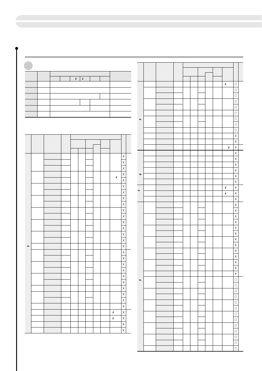
Condition
I
F
(mA)
typ
max
typ
typ
SEL1110R
SEL1110W
SEL1110S
SEL1610W
SEL1610C
SEL1210R
SEL1210S
SEL1810D
SEL1810A
SEL1910D
SEL1910A
SEL1710Y
SEL1710K
SEL1410G
SEL1410E
SEL1510C
SEL1210RM
SEL1210SM
SEL1810DM
SEL1810AM
SEL1910DM
SEL1910AM
SEL1710KM
SEL1410GM
SEL1410EM
SEL1510CM
SELU1210CXM
SELU1810CXM
SELU1D10CXM
SELU1E10CXM
Deep red
Red
Amber
Orange
Yellow
Green
Pure green
Red
Amber
Orange
Yellow
Green
Pure green
2.0
1.75
1.9
1.9
1.9
2.0
2.0
2.0
1.9
1.9
1.9
2.0
2.0
2.0
2.0
2.0
3.3
3.3
2.5
2.2
2.5
2.5
2.5
2.5
2.5
2.5
2.5
2.5
2.5
2.5
2.5
2.5
2.5
2.5
4.0
4.0
5
20
20
10
10
10
20
20
20
10
10
10
20
20
20
20
20
20
700
660
630
610
587
570
560
555
630
610
587
570
560
555
635
615
525
470
GaP
GaA As
GaAsP
GaAsP
GaAsP
GaP
GaP
GaP
GaAsP
GaAsP
GaAsP
GaP
GaP
GaP
A GaInP
A GaInP
InGaN
InGaN
1
2
3
2.8
2.8
4.5
1000
1200
26
75
18
37
14
25
22
65
32
84
50
36
75
18
37
19
34
65
30
84
50
280
570
2000
600
SELU1250CM
SEL1250SM
SEL1250RM
SEL1850AM
SEL1850DM
SEL1950KM
SEL1450EKM
SEL1450GM-YG
SEL1550CM
SELU1D50CM
SELU1E50CM
SEL1615C
SEL1111R
SEL1211R
SEL1811D
SEL1911D
SEL1711Y
SEL1411G
SELU1253CMKT
SELU1853CMKT
SEL1453CEMKT
SEL4110S
SEL4110R
SEL4210S
SEL4210R
SEL4810A
SEL4810D
SEL4910A
SEL4910D
SEL4710K
SEL4710Y
SEL4410E
SEL4410G
SEL4510C
SEL4114S
SEL4114R
SEL4214S
SEL4214R
SEL4814A
SEL4814D
SEL4914A
SEL4914D
SEL4714K
SEL4714Y
SEL4414E
SEL4414G
SEL4514C
Red
Amber
Orange
Green
Pure green
Deep red
Red
Amber
Orange
Yellow
Green
Green
Deep red
Red
Amber
Orange
Yellow
Green
Pure green
Deep red
Red
Amber
Orange
Yellow
Green
Pure green
2.0
1.9
1.9
1.9
2.0
2.0
3.3
3.3
1.75
2.0
1.9
1.9
1.9
2.0
2.0
2.0
2.0
2.0
2.0
1.9
1.9
1.9
2.0
2.0
2.0
2.0
1.9
1.9
1.9
2.0
2.0
2.0
2.5
2.5
2.5
2.5
2.5
2.5
4.0
4.0
2.2
2.5
2.5
2.5
2.5
2.5
2.5
2.5
2.5
2.5
2.5
2.5
2.5
2.5
2.5
2.5
2.5
2.5
2.5
2.5
2.5
2.5
2.5
2.5
20
20
20
20
20
20
20
20
20
10
20
10
10
10
20
20
20
20
5
20
10
10
10
20
20
10
20
10
10
10
20
20
635
630
610
587
560
555
525
470
660
700
630
610
587
570
560
635
615
560
700
630
610
587
570
560
555
700
630
610
587
570
560
555
A GaInP
GaAsP
GaAsP
GaAsP
GaP
GaP
InGaN
InGaN
GaA As
GaP
GaAsP
GaAsP
GaAsP
GaP
GaP
A GaInP
A GaInP
GaP
GaP
GaAsP
GaAsP
GaAsP
GaP
GaP
GaP
GaP
GaAsP
GaAsP
GaAsP
GaP
GaP
GaP
4
5
6
7
8
9
900
75
48
90
60
96
190
120
72
6000
1850
700
1.4
12
8.0
8.0
13
30
200
450
140
2.4
1.7
30
17
20
15
26
16
36
14
87
34
45
3.8
2.8
40
24
20
15
26
11
38
27
69
48
26
Condition
I
F
(mA)
typ
max
typ
typ
119
General-purpose LEDs
Parameter
Unit
Ratings
mA
mA/ºC
mA
V
ºC
ºC
I
F
∆
I
F
I
FP
V
R
Top
Tstg
Ratings
GaP
GaAsP GaA As A GaInP InGaN
GaN
30
–0.45
Above 25ºC
f=1kHz, tw=100
µ
s
70
100
4
5
3
–30 to +85
–25 to +85
–30 to +100
(Ta=25ºC)
Absolute Maximum Ratings
Uni-Color LED Lamp
Diffused
red
Diffused
white
Diffused
white
Tinted
red
Diffused
red
Tinted
red
Diffused
orange
Tinted
orange
Diffused
orange
Tinted
orange
Diffused
yellow
Tinted
yellow
Diffused
green
Tinted
green
Clear
Diffused
red
Tinted
red
Diffused
orange
Tinted
orange
Diffused
orange
Tinted
orange
Tinted
yellow
Diffused
green
Tinted
green
Clear
Clear
Clear
Clear
Clear
Tinted
red
Diffused
red
Tinted
orange
Diffused
orange
Tinted
orange
Tinted
green
Diffused
green
Diffused
red
Diffused
red
Diffused
orange
Diffused
orange
Diffused
yellow
Diffused
green
Tinted
green
Tinted
red
Diffused
red
Tinted
red
Diffused
red
Tinted
orange
Diffused
orange
Tinted
orange
Diffused
orange
Tinted
yellow
Diffused
yellow
Tinted
green
Diffused
green
Tinted
red
Diffused
red
Tinted
red
Diffused
red
Tinted
orange
Diffused
orange
Tinted
orange
Diffused
orange
Tinted
yellow
Diffused
yellow
Tinted
green
Diffused
green
High-
intensity red
High-
intensity red
Ultra high-
intensity blue
Ultra high-
intensity pure green
Ultra high-
intensity red
Ultra high-
intensity red
Ultra high-
intensity red
Ultra high-
intensity amber
Ultra high-
intensity pure green
Ultra high-
intensity blue
Ultra high-
intensity amber
5 Round
5 Round
4 Round
Outline
Emitting
color
Lens
color
Part No.
V
F
(V)
I
V
λ
p
(nm)
(mcd)
Electro-optical characteristics (Ta=25ºC)
Chip
material
Fig. No.
Contact mount
4.6
✕
5.6
Egg-shaped
5 Cylindrical
Outline
Emitting
color
Lens
color
Part No.
V
F
(V)
I
V
λ
p
(nm)
(mcd)
Electro-optical characteristics (Ta=25ºC)
Chip
material
Fig. No.
Contact mount
Clear
Clear
Clear
Clear
Clear
Clear
Clear
Clear
Clear
Clear
120
Condition
I
F
(mA)
typ
max
typ
typ
SEL6110S
SEL6110R
SEL6210S
SEL6210R
SEL6810A
SEL6810D
SEL6910A
SEL6910D
SEL6710K
SEL6710Y
SEL6410E
SEL6410G
SEL6510C
SEL6510G
SEL6214S
SEL6814A
SELS6B14C
SEL6914A
SEL6914W
SEL6714K
SEL6714W
SEL6414E
SEL6414E-TG
SEL6514C
SEL6215S
SEL6915A
SEL6715C
SEL6415E
SEL6515C
SEL2110S
SEL2110R
SEL2110W
SEL2610C
SEL2210S
SEL2210R
SEL2210W
SEL2810A
SEL2810D
SEL2910A
SEL2910D
SELU2710C
SEL2710K
SEL2710Y
SEL2410E
SEL2410G
Deep red
Red
Amber
Orange
Yellow
Green
Pure green
Red
Amber
Orange
Yellow
Green
Deep green
Pure green
Red
Orange
Yellow
Green
Pure green
Deep red
Red
Amber
Orange
Yellow
Green
2.0
1.9
1.9
1.9
2.0
2.0
2.0
1.9
1.9
2.0
1.9
2.0
2.0
2.0
1.9
1.9
2.0
2.0
2.0
2.0
1.75
1.9
1.9
1.9
2.0
2.0
2.0
2.5
2.5
2.5
2.5
2.5
2.5
2.5
2.5
2.5
2.5
2.5
2.5
2.5
2.5
2.5
2.5
2.5
2.5
2.5
2.5
2.2
2.5
2.5
2.5
2.5
2.5
2.5
10
20
10
10
10
20
20
20
10
20
10
20
20
20
20
20
20
20
20
10
20
20
10
10
20
10
20
700
630
610
587
570
560
555
630
610
600
587
570
560
558
555
630
587
570
560
555
700
660
630
610
587
572
570
560
GaP
GaAsP
GaAsP
GaAsP
GaP
GaP
GaP
GaAsP
GaAsP
A GaInP
GaAsP
GaP
GaP
GaP
GaAsP
GaAsP
GaP
GaP
GaP
GaP
GaA As
GaAsP
GaAsP
GaAsP
A GaInP
GaP
GaP
10
11
12
13
3.9
2.6
41
18
22
9.6
22
11
37
11
90
30
42
9.6
18
9.0
120
8.0
5.0
66
30
42
18
12
45
60
90
81
44
4
1.8
1.8
350
40
15
15
22
9.0
16
8.0
270
40
14
77
20
SEL2510C
SEL2510G
SELU2D10C
SELU2E10C
SEL2E10C
SEL2215S
SEL2215R
SEL2815A
SEL2815D
SEL2915A
SEL2915D
SEL2715K
SEL2715Y
SEL2415E
SEL2415G
SEL2515C
SEL2111R
SEL2911D
SEL2411G
SEL4117R
SEL4817D
SEL4917D
SEL4717Y
SEL4417G
SEL1213C
SEL1813A
SEL1913K
SEL1713K
SEL1413E
SEL1513E
SEL6413E
SEL6513C
SEL2613CS-S
SEL2213C
SEL2813A
SEL2913K
SEL2713K
SEL2413E
SEL2413G
SEL2513E
SEL1121R
SEL1821D
SEL1921D
SEL1721Y
SEL1421G
Pure green
Blue
Red
Amber
Orange
Yellow
Green
Pure green
Deep red
Orange
Green
Deep red
Amber
Orange
Yellow
Green
Red
Amber
Orange
Yellow
Green
Pure green
Green
Pure green
Red
Amber
Orange
Yellow
Green
Pure green
Deep red
Amber
Orange
Yellow
Green
2.0
3.3
3.3
3.8
1.9
1.9
1.9
2.0
2.0
2.0
2.0
1.9
2.0
2.0
1.9
1.9
2.0
2.0
1.9
1.9
1.9
2.0
2.0
2.0
2.0
2.0
1.7
1.9
1.9
1.9
2.0
2.0
2.0
2.0
1.9
1.9
2.0
2.0
2.5
4.0
4.0
4.8
2.5
2.5
2.5
2.5
2.5
2.5
2.5
2.5
2.5
2.5
2.5
2.5
2.5
2.5
2.5
2.5
2.5
2.5
2.5
2.5
2.5
2.5
2.5
2.5
2.5
2.5
2.5
2.5
2.5
2.5
2.5
2.5
2.5
2.5
20
20
20
20
20
10
10
10
20
20
10
10
20
10
10
10
20
20
20
20
20
20
20
20
20
20
20
20
20
20
20
20
20
10
10
10
10
20
555
525
470
430
630
610
587
570
560
555
700
587
560
700
610
587
570
560
630
610
587
570
560
555
560
555
660
630
610
587
570
560
555
700
610
587
570
560
GaP
InGaN
InGaN
GaN
GaAsP
GaAsP
GaAsP
GaP
GaP
GaP
GaP
GaAsP
GaP
GaP
GaAsP
GaAsP
GaP
GaP
GaAsP
GaAsP
GaAsP
GaP
GaP
GaP
GaP
GaP
GaA As
GaAsP
GaAsP
GaAsP
GaP
GaP
GaP
GaP
GaAsP
GaAsP
GaP
GaP
13
14
15
16
17
18
19
20
43
8.2
1200
400
60
45
38
80
60
81
53
130
110
110
72
52
0.7
3.3
18
1.1
7.5
7.5
14
16
7.0
8.0
8.0
15
12
5.0
14
5.0
80
7.0
8.0
8.0
17
14
12
5.0
0.9
3.0
3.8
7.0
12
Condition
I
F
(mA)
typ
max
typ
typ
Uni-Color LED Lamp
Diffused
red
Tinted
red
Diffused
red
Tinted
orange
Diffused
orange
Tinted
orange
Diffused
orange
Tinted
yellow
Diffused
yellow
Tinted
green
Diffused
green
Clear
Diffused
green
Tinted
red
Tinted
orange
Clear
Tinted
orange
Tinted
yellow
Tinted
green
Tinted
green
Clear
Tinted
red
Tinted
orange
Clear
Tinted
green
Clear
Tinted
red
Diffused
red
Clear
Tinted
red
Diffused
red
Tinted
orange
Diffused
orange
Tinted
orange
Diffused
orange
Clear
Tinted
yellow
Diffused
yellow
Tinted
green
Diffused
green
Tinted
red
Clear
Diffused
green
Clear
Clear
Clear
Tinted
red
Diffused
red
Tinted
orange
Diffused
orange
Tinted
orange
Diffused
orange
Tinted
yellow
Diffused
yellow
Tinted
green
Diffused
green
Clear
Diffused
red
Diffused
orange
Diffused
green
Diffused
red
Diffused
orange
Diffused
orange
Diffused
yellow
Diffused
green
Tinted
red
Tinted
orange
Tinted
light orange
Tinted
yellow
Tinted
green
Tinted
green
Clear
Clear
Tinted
orange
Tinted
light orange
Tinted
light red
Tinted
light green
Tinted
yellow
Tinted
green
Diffused
green
Tinted
green
Diffused
red
Diffused
orange
Diffused
orange
Diffused
yellow
Diffused
green
High-
intensity red
High-
intensity red
Ultra high-
intensity blue
Ultra high-
intensity pure green
Ultra high-
intensity yellow
Outline
Emitting
color
Lens
color
Part No.
V
F
(V)
I
V
λ
p
(nm)
(mcd)
Electro-optical characteristics (Ta=25ºC)
Chip
material
Fig. No.
Contact mount
Outline
Emitting
color
Lens
color
Part No.
V
F
(V)
I
V
λ
p
(nm)
(mcd)
Electro-optical characteristics (Ta=25ºC)
Chip
material
Fig. No.
Contact mount
General-purpose LEDs
3 Round
3 Round
2 Round
Inverted-cone typ for surface illumination
3
✕
5
Rectangular
3 Cylindrical
Ultra-high-
intensiti
light amber
Diffused
white
Diffused
white
Diffused
white
Diffused
white
Condition
I
F
(mA)
typ
max
typ
typ
SEL1222R
SEL1822D
SEL1922D
SEL1722Y
SEL1722K
SEL1422G
SEL1120R
SEL1220R
SEL1820D
SEL1920D
SEL1720Y
SEL1420G
SEL1124R
SEL1824D
SEL1924D
SEL1724Y
SEL1424G
SEL4225C
SEL4225R
SEL4825A
SEL4825D
SEL4925A
SEL4925D
SEL4725K
SEL4725Y
SEL4425E
SEL4425G
SEL4525C
SEL4226C
SEL4226R
SEL4826A
SEL4826D
SEL4926A
SEL4926D
SEL4726K
SEL4726Y
SEL4426E
SEL4426G
SEL4227C
SEL4427EP
SEL6227S
SEL6927A
SEL6427EP
Red
Amber
Orange
Yellow
Green
Deep red
Red
Amber
Orange
Yellow
Green
Deep red
Amber
Orange
Yellow
Green
Red
Amber
Orange
Yellow
Green
Pure green
Red
Amber
Orange
Yellow
Green
Red
Green
Red
Orange
Green
1.9
1.9
1.9
2.0
2.0
2.0
1.9
1.9
1.9
2.0
2.0
2.0
1.9
1.9
2.0
2.0
1.9
1.9
1.9
2.0
2.0
2.0
1.9
1.9
1.9
2.0
2.0
1.9
2.0
1.9
1.9
2.0
2.5
2.5
2.5
2.5
2.5
2.5
2.5
2.5
2.5
2.5
2.5
2.5
2.5
2.5
2.5
2.5
2.5
2.5
2.5
2.5
2.5
2.5
2.5
2.5
2.5
2.5
2.5
2.5
2.5
2.5
2.5
2.5
20
10
10
10
20
10
20
10
10
10
20
10
10
10
10
20
20
10
10
10
20
20
20
10
10
10
20
20
20
20
10
20
630
610
587
570
560
700
630
610
587
570
560
700
610
587
570
560
630
610
587
570
560
555
630
610
587
570
560
630
560
630
587
560
GaAsP
GaAsP
GaAsP
GaP
GaP
GaP
GaAsP
GaAsP
GaAsP
GaP
GaP
GaP
GaAsP
GaAsP
GaP
GaP
GaAsP
GaAsP
GaAsP
GaP
GaP
GaP
GaAsP
GaAsP
GaAsP
GaP
GaP
GaAsP
GaP
GaAsP
GaAsP
GaP
21
22
23
24
25
26
27
9.0
4.8
4.5
7.8
12
7.2
0.9
4.8
3.0
3.8
7.0
11
0.5
4.0
3.0
6.0
15
12
5.4
5.4
4.0
4.5
4.0
13
5.0
20
10
6.6
12
10
5.4
4.5
6.0
4.5
14
8.6
20
14
15
19
14
10
26
SEL4628C-S
SEL4228C
SEL4828A
SEL4928A
SEL4728K
SEL4428E
SEL4428B-TG
SEL4528C
SEL4229R
SEL4829A
SEL4929A
SEL4729KH
SEL4429E
SEL5620C
SEL5220S
SEL5820A
SEL5920A
SEL5420E
SEL5520C
SELU5E20C
SEL5221S
SEL5821A
SEL5921A
SEL5721C
SEL5421E
SEL5521C
SELS5223C
SEL5223S
SELS5823C
SELU5823C
SEL5823A
SELS5B23C
SELS5923C
SEL5923A
SELU5723C
SEL5723C
SEL5423E
SEL5523C
SELU5E23C
SEL5E23C
SEL5255S
SEL5955A
SEL5755C
Red
Amber
Orange
Yellow
Green
Deep green
Pure green
Red
Amber
Orange
Yellow
Green
Red
Amber
Orange
Green
Pure green
Red
Amber
Orange
Yellow
Green
Pure green
Red
Amber
Orange
Yellow
Green
Pure green
Blue
Red
Orange
Yellow
1.7
1.9
1.9
1.9
2.0
2.0
2.0
2.0
1.9
1.9
1.9
2.0
2.0
1.7
1.9
1.9
1.9
2.0
2.0
3.3
1.9
1.9
1.9
2.0
2.0
2.0
2.0
1.9
2.0
1.9
2.0
2.0
1.9
2.0
2.0
2.0
2.0
3.6
4.0
1.9
1.9
2.0
2.2
2.5
2.5
2.5
2.5
2.5
2.5
2.5
2.5
2.5
2.5
2.5
2.5
2.2
2.5
2.5
2.5
2.5
2.5
4.0
2.5
2.5
2.5
2.5
2.5
2.5
2.5
2.5
2.5
2.5
2.5
2.5
2.5
2.5
2.5
2.5
2.5
4.0
4.8
2.5
2.5
2.5
20
20
10
10
10
20
20
20
20
10
10
10
20
20
20
20
20
20
20
10
20
20
20
20
20
20
20
20
20
20
20
20
20
20
20
20
20
10
20
20
20
20
660
630
610
587
570
560
558
555
630
610
587
570
560
660
630
610
587
560
555
470
630
610
587
570
560
555
635
630
615
610
600
590
587
572
570
560
555
470
430
630
587
570
GaA As
GaAsP
GaAsP
GaAsP
GaP
GaP
GaP
GaP
GaAsP
GaAsP
GaAsP
GaP
GaP
GaA As
GaAsP
GaAsP
GaAsP
GaP
GaP
InGaN
GaAsP
GaAsP
GaAsP
GaP
GaP
GaP
A GaInP
GaAsP
A GaInP
GaAsP
A GaInP
A GaInP
GaAsP
A GaInP
GaP
GaP
GaP
InGaN
GaN
GaAsP
GaAsP
GaP
28
29
30
31
32
33
200
27
14
14
30
63
18
30
21
18
18
60
60
100
20
12
12
20
6.0
60
35
60
60
90
95
35
100
25
130
185
35
135
145
35
155
60
40
13
110
20
35
25
140
Condition
I
F
(mA)
typ
max
typ
typ
121
Diffused
red
Diffused
orange
Diffused
orange
Diffused
yellow
Tinted
yellow
Diffused
green
Diffused
red
Diffused
red
Diffused
orange
Diffused
orange
Diffused
yellow
Diffused
green
Diffused
red
Diffused
orange
Diffused
orange
Diffused
yellow
Diffused
green
Clear
Diffused
red
Tinted
orange
Diffused
orange
Tinted
orange
Diffused
orange
Tinted
yellow
Diffused
yellow
Tinted
green
Diffused
green
Clear
Clear
Diffused
red
Tinted
orange
Diffused
orange
Tinted
orange
Diffused
orange
Tinted
yellow
Diffused
yellow
Tinted
green
Diffused
green
Clear
Tinted
green
Tinted
red
Tinted
orange
Tinted
green
Clear
Clear
Tinted
orange
Tinted
orange
Tinted
yellow
Tinted
dark blue
Tinted
green
Clear
Diffused
red
Tinted
orange
Tinted
orange
Tinted
yellow
Tinted
green
Clear
Tinted
red
Tinted
orange
Tinted
orange
Tinted
green
Clear
Clear
Tinted
red
Tinted
orange
Tinted
orange
Clear
Tinted
green
Clear
Clear
Tinted
red
Clear
Clear
Tinted
orange
Clear
Clear
Tinted
orange
Clear
Clear
Tinted
green
Clear
Clear
Clear
Tinted
red
Tinted
orange
Clear
High-
intensity red
High-
intensity red
Ultra high-
intensity red
Ultra high-
intensity blue
Ultra high-
intensity yellow
Ultra high-
intensity amber
Ultra high-
intensity orange
Ultra high-
intensity blue
Uni-Color LED Lamp
General-purpose LEDs
Outline
Emitting
color
Lens
color
Part No.
V
F
(V)
I
V
λ
p
(nm)
(mcd)
Electro-optical characteristics (Ta=25ºC)
Chip
material
Fig. No.
Contact mount
Outline
Emitting
color
Lens
color
Part No.
V
F
(V)
I
V
λ
p
(nm)
(mcd)
Electro-optical characteristics (Ta=25ºC)
Chip
material
Fig. No.
Contact mount
2.5
✕
5
Rectangular
2
✕
5
Rectangular
1
✕
5
Rectangular
2
✕
4 Rectangular
4 Bow-shaped
3.1 Bow-shaped
5mm Pitch lead rectangular
5mm Pitch lead 3
lens-type
5mm Pitch lead bow-shaped
5mm Pitch lead
egg-shaped
Ultra-high-
intensiti
light amber
Condition
I
F
(mA)
typ
max
typ
typ
SML11516C
SML1216C
SML1216W
SML1516W
SML16716CN
SML16716WN
SML1816W
SML19416W
SML12451W
SML16751WN
SML12460C
SML16760CN
SML19460C
SML72420C
SML78420C
SML79420C
Deep red
Pure green
Red
Green
Red
Green
Deep red
Pure green
Yellow
Yellow
Amber
Green
Orange
Green
Red
Green
Yellow
Red
Green
Yellow
Orange
Green
Red
Green
Amber
Green
Orange
Green
A
B
A
B
A
B
A
B
A
B
A
B
A
B
A
B
A
B
A
B
A
B
A
B
A
B
A
B
A
B
A
B
Red
Green
Red
Orange
Amber
Green
Orange
Green
Yellow
Red
Yellow
Orange
Red
Orange
Green
Yellow
A
B
A
B
A
B
A
B
A
B
A
B
A
B
A
B
A
B
A
B
A
B
2.0
2.0
1.9
2.0
1.9
2.0
2.0
2.0
1.7
2.4
1.7
2.4
1.9
2.0
1.9
2.0
1.9
2.0
1.7
2.4
1.9
2.0
1.7
2.4
1.9
2.0
1.9
2.0
1.9
2.0
1.9
2.0
2.5
2.5
2.5
2.5
2.5
2.5
2.5
2.5
2.2
3.0
2.2
3.0
2.5
2.5
2.5
2.5
2.5
2.5
2.2
3.0
2.5
2.5
2.2
3.0
2.5
2.5
2.5
2.5
2.5
2.5
2.5
2.5
20
20
20
20
20
20
20
20
20
20
20
20
20
20
20
20
20
20
20
20
20
20
20
20
20
20
20
20
20
20
20
20
700
555
630
560
630
560
700
555
660
570
660
570
610
560
587
560
630
560
660
570
630
560
660
570
587
560
630
560
610
560
587
560
Cathode
Cathode
Cathode
Cathode
Anode
Anode
Cathode
Cathode
Cathode
Anode
Cathode
Anode
Cathode
Cathode
Cathode
Cathode
34
35
36
37
15
50
65
90
60
60
6.0
20
100
140
50
70
50
60
45
60
40
60
50
60
10
25
30
40
15
25
15
20
10
20
10
20
122
Parameter
Unit
Conditions
mA
mA/ºC
mA
V
ºC
ºC
I
F
∆
I
F
I
FP
V
R
Top
Tstg
Ratings
Above 25ºC
f=1kHz, tw=100
µ
s
30
–0.45
100
4
–30 to +85
–30 to +100
(Ta=25ºC)
Absolute Maximum Ratings
Bi-Color LED Lamp
Condition
I
F
(mA)
typ
max
typ
typ
SML72423C
SML72923C
SML78423C
SML79423C
SMLS79723C
SML72755C
SML79255C
SML79455C
SML76755WN
SMLU72755C
SMLU78755C
1.9
2.0
1.9
1.9
1.9
2.0
1.9
2.0
2.0
2.0
1.9
2.0
1.9
2.0
1.9
2.0
1.7
2.4
2.0
2.0
2.0
2.0
2.5
2.5
2.5
2.5
2.5
2.5
2.5
2.5
2.5
2.5
2.5
2.5
2.5
2.5
2.5
2.5
2.2
3.0
2.5
2.5
2.5
2.5
20
20
20
20
20
20
20
20
20
20
20
20
20
20
20
20
20
20
20
20
20
20
630
560
630
587
610
560
587
560
590
570
630
570
587
630
587
560
660
570
635
572
615
572
Cathode
Cathode
Cathode
Cathode
Cathode
Cathode
Cathode
Cathode
Anode
Cathode
Cathode
38
39
25
35
25
25
25
35
25
35
150
40
45
75
40
45
45
75
50
50
160
170
280
170
■
Internal wiring diagram
A
1
2
3
B
Clear
Clear
Clear
Clear
Clear
Clear
Clear
Clear
Clear
Clear
Clear
Clear
Clear
Clear
Clear
Clear
Clear
Clear
Clear
High-
intensity red
Ultra high-
intensity orange
High-
intensity red
High-
intensity red
High-
intensity red
High-
intensity red
Ultra high-
intensity red
Ultra high-
intensity yellow
Ultra high-
intensity amber
Ultra high-
intensity yellow
5 Round
General-purpose LEDs
Outline
Emitting
color
Lens
color
Part No.
V
F
(V)
I
V
λ
p
(nm)
(mcd)
Electro-optical characteristics (Ta=25ºC)
Common
Fig. No.
Contact mount
Outline
Emitting
color
Lens
color
Part No.
V
F
(V)
I
V
λ
p
(nm)
(mcd)
Electro-optical characteristics (Ta=25ºC)
Common
Fig. No.
Contact mount
2.5
✕
5
Rectangular
3.3
✕
6 Rectangular
Egg-shaped
3.3
✕
6 Bow-shaped
Diffused
white
Diffused
white
Diffused
white
Diffused
white
Diffused
white
Diffused
white
Diffused
white
Diffused
white
123
Condition
I
F
(mA)
typ
max
typ
typ
SEC1101C
SEC1601C
SEC1201C
SEC1801C
SEC1901C
SEC1701C-YG
SEC1401C
SEC1401E-TG
SEC1501C
SECU1D01C
SECU1E01C
SEC1E01C
SEC1603C
SECS1203C
SEC1203C
SELS1803C
SEC1803C
SELS1903C
SEC1903C
SEC1703C
SEC1403C
SEC1403E-TG
SEC1503C
Deep red
Red
Amber
Orange
Yellow
Green
Deep reen
Pure green
Blue
Red
Amber
Orange
Yellow
Green
Deep green
Pure green
2.0
1.7
1.9
1.9
1.9
2.0
2.0
2.0
2.0
3.3
3.3
3.9
1.7
1.9
1.9
1.9
1.9
1.9
1.9
2.0
2.0
2.0
2.0
2.5
2.2
2.5
2.5
2.5
2.5
2.5
2.5
2.5
4.0
4.0
4.8
2.2
2.5
2.5
2.5
2.5
2.5
2.5
2.5
2.5
2.5
2.5
20
20
20
20
20
20
20
20
20
20
20
20
20
20
20
3
20
3
20
20
20
20
20
700
660
630
610
587
570
560
558
555
525
470
430
660
635
630
615
610
590
587
570
560
558
555
GaP
GaA As
GaAsP
GaAsP
GaAsP
GaP
GaP
GaP
GaP
InGaN
InGaN
GaN
GaA As
A GaInP
GaAsP
A GaInP
GaAsP
A GaInP
GaAsP
GaP
GaP
GaP
GaP
40
41
1.5
100
10
16
13
25
22
11
8.0
150
50
6.0
150
100
15
10
20
10
15
35
33
15
10
Parameter
Unit
Conditions
mA
mA/ºC
mA
V
ºC
ºC
I
F
∆
I
F
I
FP
V
R
Top
Tstg
Ratings
GaP
GaAsP
InGaN
GaN
30
–0.45
70
Above 25ºC
f=1kHz, tw=100
µ
s
4
5
–30 to +85
–25 to +85
–30 to +100
(Ta=25ºC)
Absolute Maximum Ratings
■
Uni-Color
Surface Mount LED
(mcd)
Condition
I
F
(mA)
typ
max
typ
typ
Electro-optical characteristics (Ta=25ºC)
SEC2422C
SEC2442C
SEC2462C
SEC2492C
SEC2552C
SEC2592C
SEC2762C-YG
SEC2484C
SEC2554C
SEC2494C
SEC2764C
SEC2774C
Red
Green
Green
Green
Green
Orange
Green
Pure green
Pure green
Orange
Pure green
Yellow
Amber
Green
Pure green
Pure green
Orange
Green
Yellow
Yellow
Yellow
A
B
A
B
A
B
A
B
A
B
A
B
A
B
A
B
A
B
A
B
A
B
A
B
1.9
2.0
2.0
2.0
1.7
2.0
1.9
2.0
2.0
2.0
1.9
2.0
1.7
2.0
1.9
2.0
2.0
2.0
1.9
2.0
1.7
2.0
2.0
2.0
2.5
2.5
2.5
2.5
2.2
2.5
2.5
2.5
2.5
2.5
2.5
2.5
2.2
2.5
2.5
2.5
2.5
2.5
2.5
2.5
2.2
2.5
2.5
2.5
20
20
20
20
20
20
20
20
20
20
20
20
20
20
20
20
20
20
20
20
20
20
20
20
630
560
560
560
660
560
587
560
555
555
587
555
660
570
610
560
555
555
587
560
660
570
570
570
42
43
10
20
20
20
20
20
10
20
5.0
5.0
10
5.0
20
20
20
30
10
10
20
30
50
50
50
50
■
Bi-Color
■
Internal wiring diagram
A
B
1
2
4
3
GaA As A GaInP
Fig. No.
Fig. No.
Clear
Clear
Clear
Clear
Clear
Clear
Clear
Tinted
green
Clear
Clear
Clear
Clear
Clear
Clear
Clear
Clear
Clear
Clear
Clear
Clear
Clear
Clear
Clear
Clear
Clear
Clear
Clear
Clear
Clear
Clear
Clear
Clear
Clear
Clear
Clear
High-
intensity red
High-
intensity red
High-
intensity red
High-
intensity red
High-
intensity red
Ultra high-
intensity red
Ultra high-
intensity amber
Ultra high-
intensity orange
Ultra high-
intensity pure green
Ultra high-
intensity blue
Inner lens type
Flat lens type
Inner lens type
F
lat lens type
General-purpose LEDs
Outline
Outline
Emitting
color
Emitting
color
Lens
color
Lens
color
Part No.
Part No.
V
F
(V)
I
V
V
F
(V)
I
V
λ
p
(nm)
λ
p
(nm)
(mcd)
Electro-optical characteristics (Ta=25ºC)
Chip
material
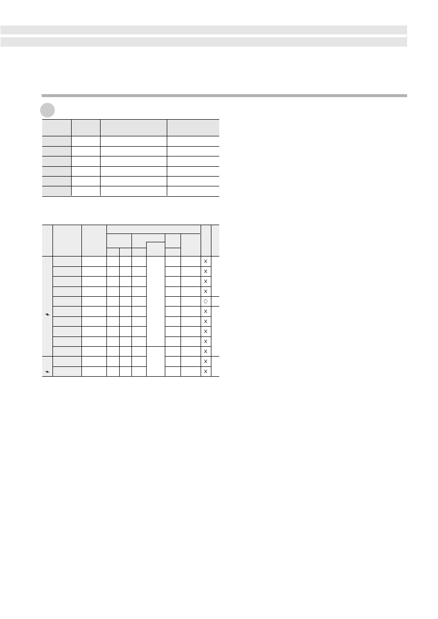
124
Ie
(mW/sr)
Condition
typ
max
typ
typ
SID1010CM
SID1K10CM
SID1010CXM
SID1K10CXM
SID1050CM
SID303C
SID313BP
SID1003BQ
SID307BR
SID1G307C
SID2010C
SID2K10C
1.3
1.3
1.3
1.3
1.3
1.3
1.3
1.3
1.3
1.5
1.3
1.3
1.5
1.5
1.5
1.5
1.5
1.5
1.5
1.5
1.5
1.8
1.5
1.5
940
940
940
940
940
940
940
940
940
850
940
940
GaAs
GaAs
GaAs
GaAs
GaAs
GaAs
GaAs
GaAs
GaAs
GaAs
GaAs
GaAs
44
45
46
47
130
200
60
110
250
80
130
180
200
50
7.0
14
(Constant
voltage)
V
CC
=3V,
R=2.2
Ω
Parameter
Unit
Ratings
mA
mA/ºC
mA
V
ºC
ºC
I
F
∆
I
F
I
FP
V
R
Top
Tstg
Ratings
Above 25ºC
f=1kHz, tw=10
µ
s
150
–1.33
1000
5
–30 to +85
–30 to +100
(Ta=25ºC)
Absolute Maximum Ratings
Infrared LED
I
F
=50mA
Fig. No.
Clear
Clear
Clear
Clear
Clear
Clear
Transparent
light purpl
Transparent
light navy blue
Transparent
dark navy blue
Clear
Clear
Clear
5 Round
3 Round
General-purpose LEDs
Outline
Lens
color
Part No.
V
F
(V)
λ
p
(nm)
Electro-optical characteristics (Ta=25ºC)
Chip
material
Contact mount

Fig. 1
Fig. 2
Fig. 3
Fig. 4
Fig. 5
Fig. 6
Fig. 7
Fig. 8
Fig. 9
Fig. 10
General-purpose LEDs - External Dimensions
5.6
±
0.2
20.0min 5.0
±
0.5
7.6
±
0.2
19.0min 0.8
(1.0)
Cathode
0.5
(2.54)
0.5
1.1max
0.8
Resin heap 1.5max
5.0
±
0.2
0.5
±
0.1
Anode
Cathode
1.0min
21.0min
9.4
±
0.3
5.0
±
0.2
Resin heap 0.8max
Resin burr 0.3max
0.65
max
0.5
±
0.1
(2.54)
5.6
±
0.2
20.0min 5.5
±
0.5
8.2
±
0.2
19.0min 0.8
(1.0)
Cathode
0.5
±
0.1
1.1max
0.8
Resin heap 1.5max
5.0
±
0.2
0.5
(2.54)
5.6
±
0.2
23.0min
1.0min
6.9
±
0.2
Cathode
0.65max
Resin heap 1.5max
5.0
±
0.2
(2.54)
0.5
±
0.1
(1.0)
0.5
±
0.1
5.6
±
0.2
23.0min
1.0min
7.6
±
0.2
Cathode
0.65max
Resin heap 1.5max
5.0
±
0.2
0.5
±
0.1
0.5
±
0.1
(1.0)
(2.54)
2.2
4.8
0.4
±
0.1
(2.54)
0.45
±
0.1
1.1max
Resin heap 1.5max
Cathode
1.0min
25.5min
5.0
±
0.2
6.5
±
0.5
0.8
1.5
4.0
±
0.2
2.2
4.8
(2.54)
0.45
±
0.1
0.65max
Resin heap 0.8max
1.0min
24.5min
5.0
±
0.2
4.0
±
0.2
(1.5)
0.4
±
0.1
Cathode
3.5
0.8
±
0.2
4.0
±
0.2
0.4
±
0.1
23.0min
1.0min
5.5
±
0.5
(1.7)
3.5
±
0.1
(2.54)
3.1
±
0.1
4.4
0.45
±
0.1
0.65max
Resin heap
0.8max
Cathode
5.6
±
0.2
20.0min 5.0
±
0.5
7.9
±
0.2
19.0min 0.8
(1.0)
Cathode
0.5
(2.54)
0.5
±
0.1
1.1max
0.8
Resin heap 1.5max
5.0
±
0.2
5.6
±
0.2
Resin burr 0.3max
4.6
±
0.2
1.0min
23.5min
Cathode
Anode
7.7
±
0.5
(2.54)
0.65max
4.7
±
0.2
5.7
±
0.2
2-0.5
±
0.1
0.5
±
0.1
Resin heap 1.5max
125
(Unit: mm)
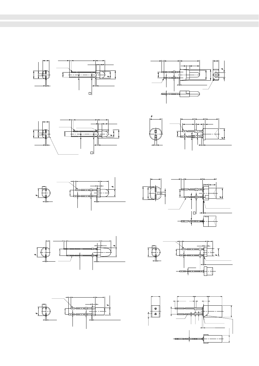
Fig. 11
Fig. 12
Fig. 13
Fig. 14
Fig. 15
Fig. 16
Fig. 17
Fig. 18
Fig. 19
Fig. 20
1.7
3.8
0.4
1.0min
25.8min
3.5
±
0.1
(1.3)
0.45
±
0.1
0.65max
Resin heap 1.5max
3.1
±
0.1
Cathode
(2.54)
1.55
3.8
0.4
±
0.1
1.0min
25.4min
4.0
±
0.1
(1.3)
(2.54)
0.45
±
0.1
0.65max
Resin heap 1.5max
3.1
±
0.1
Cathode
3.5
0.8
±
0.2
4.0
±
0.2
0.4
±
0.1
23.0min
1.0min
4.5
±
0.5
(1.6)
2.5
±
0.1
(2.54)
3.5
4.4
0.45
±
0.1
0.65max
Resin heap
0.8max
Cathode
3.5
5.5
0.8
±
0.2
4.0
±
0.2
0.4
±
0.1
23.0min
1.0min
(1.7)
3.5
±
0.1
(2.54)
3.1
±
0.1
4.4
0.45
±
0.1
0.65max
Resin heap
0.8max
Resin burr
0.3max
Cathode mark
Cathode
1.7
3.8
0.4
±
0.1
(2.54)
1.0min
25.8min
4.2
±
0.1
(1.3)
0.45
±
0.1
0.65max
Resin heap 1.5max
3.1
±
0.1
Cathode
1.0min
23.0min
8.0
±
0.2
(1.5) 4.0
±
0.1
4.0
±
0.2
4.4
±
0.2
2.5
±
0.2
2.0
±
0.1
(2.54)
0.45
±
0.1
0.65max
Resin heap 1.5max
0.4
±
0.1
Cathode
C1.0
5.6
±
0.2
20.0min 5.0
±
0.5
5.8
±
0.2
19.0min 0.8
(1.0)
0.5
0.5
±
0.1
1.1max
0.8
Resin heap 1.5max
4.9
±
0.2
Cathode
(2.54)
1.7
3.8
±
0.1
0.4
(2.54)
1.0min
25.8min
2.6
±
0.1
(1.3)
0.45
±
0.1
0.65max
Resin heap 1.5max
Resin burr 0.3max
3.1
±
0.1
Cathode
0.4
±
0.1
23.0min
4.5
1.0min
3.5
2.5
±
0.1
(1.7)
0.45
±
0.1
0.8
±
0.2
4.0
±
0.2
4.4
0.65max
Resin heap 0.8max
Resin burr 0.3max
3.5
±
0.1
(2.54)
0.4
±
0.1
Cathode
±
0.1
±
0.2
±
0.2
5.0
0.8
0.5
±
0.5
±
0.2
1.5
±
0.2
3.0
3.8
0.8
6.0
(2.0)
0.5
1.1max
Resin heap 1.5max
Resin burr 0.3max
6.0
20.0min
(2.54)
1.0min
±
0.2
Cathode mark
±
0.1
Cathode
126
(Unit: mm)
General-purpose LEDs - External Dimensions
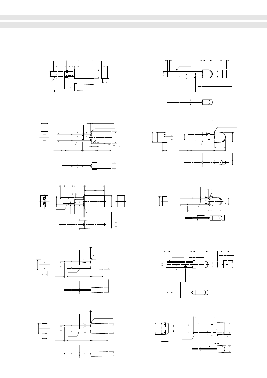
Fig. 21
Fig. 22
Fig. 23
Fig. 24
Fig. 25
Fig. 26
Fig. 27
Fig. 28
Fig. 29
Fig. 30
20.0min
(2.54)
5.0
±
0.5
9.0
±
0.2
4.0
±
0.2
19.0min 0.8
(1.0)
2.5
±
0.15
0.5
±
0.1
1.1max
0.8
5.0
±
0.2
Cathode
3.0
±
0.15
0.45
±
0.1
0.4
±
0.1
0.65max
Resin heap 0.8max
1.0min
23.0min
5.0
±
0.2
4.0
±
0.2
Cathode
2.0
±
0.1
(2.54)
0.45
0.65max
Resin heap 0.8max
1.0min
20.5min
8.0
±
0.2
3.1
±
0.2
Cathode
3.0
(1.0)
3.5
±
0.2
2.4
4.2
(2.54)
0.4
±
0.1
6.0
6.0
20.0min
1.0min
2.8
5.0
Cathode
(2.54)
2.0
Cathode mark
±
0.2
±
0.2
±
0.5
Resin heap 1.5max
(2.0)
±
0.2
0.5
±
0.1
1.1max
±
0.2
0.5
±
0.1
0.8
Resin burr 0.3max
±
0.1
±
0.15
±
0.2
0.8
±
0.2
±
0.5
1.0min
4.5
4.5
3.2
±
0.2
±
0.1
Resin burr 0.3min
1.1max
Resin heap 1.5max
4.0
4.9
8.5
1.0
2.8
19.0min
0.5
0.5
(2.54)
0.8
Cathode
±
0.2
Resin burr 0.3max
±
0.2
4.0
±
0.1
0.4
±
0.1
(2.54)
0.45
0.65max
4.3
Resin heap 0.8max
±
0.2
2.0
1.0min
2.3
5.0
23.0min
Cathode
±
0.2
±
0.2
Resin burr 0.3max
4.0
±
0.1
0.4
0.45
0.65max
±
0.1
(2.54)
4.3
Resin heap 0.8max
±
0.2
2.0
1.0min
2.3
21.0min
7.0
Cathode
(2.54)
4.0
±
0.2
2.0
±
0.1
±
0.2
Resin heap 0.8max
Resin burr 0.3max
5.0
23.5min
1.0min
0.4
±
0.1
0.65max
0.45
±
0.1
Cathode
3.1
±
0.2
±
0.2
±
0.2
Resin burr 0.3max
4.0
±
0.1
0.4
0.45
0.65max
(2.54)
±
0.1
0.8
4.4
4.0
±
0.2
±
0.2
Resin heap 0.8max
±
0.2
2.0
1.0min
2.1
4.6
4.9
23.0min
Cathode
6.2
1.4
3.6
(5.0)
4.2
±
0.5
23.0min
1.0min
6.0
±
0.2
0.5
±
0.1
0.65max
Resin heap 0.8max
Resin burr 0.3max
Cathode
3.3
±
0.2
0.5
±
0.1
Cathode mark
127
(Unit: mm)
General-purpose LEDs - External Dimensions
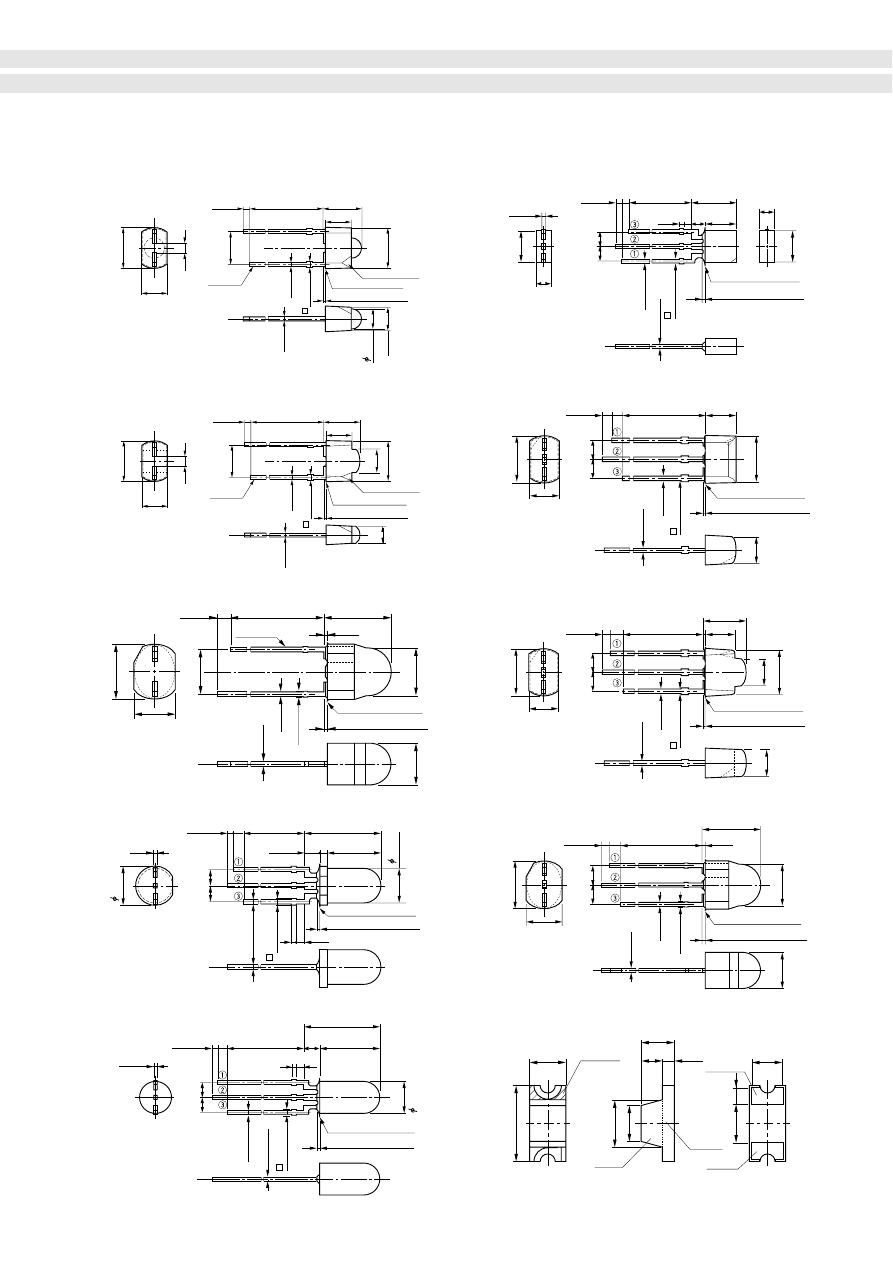
Fig. 31
Fig. 32
Fig. 33
Fig. 34
Fig. 35
Fig. 36
Fig. 37
Fig. 38
Fig. 39
Fig. 40
6.2
1.4
3.6
(5.0)
5.8
±
0.5
23.0min
1.0min
3.9
6.0
±
0.2
0.5
+0.1
0.65max
Resin heap 0.8max
Cathode mark
Cathode
0.5
±
0.1
3.2
±
0.2
3.0
±
0.2
Resin burr 0.3max
6.2
1.4
3.6
(5.0)
5.8
±
0.5
23.0min
1.0min
3.9
0.5
+0.1
0.65max
Resin heap 0.8max
Resin burr 0.3max
Cathode mark
Cathode
0.5
±
0.1
3.6
±
0.2
6.0
±
0.2
3.1
1.0min
17.0min
10.6
±
0.5
1.5min
2.0
±
0.5
7.6
±
0.2
1.0
0.5
±
0.1
5.8
±
0.2
(2.54)
(2.54)
Resin heap 1.5max
Resin burr 0.3max
5.0
±
0.2
1.2
0.8
3
–
0.5
±
0.1
0.65max
0.8
Resin heap 1.5max
0.5
±
0.1
5.2
(2.54)
(2.54)
Resin burr 0.3max
5.0
±
0.2
3
–
0.5
±
0.1
0.65max
3
–
0.5
±
0.1
2.8
1.2 (2.0)
2.5
±
0.2
1.0min
1.5min
17.0min
7.0
±
0.5
5.0
±
0.2
Resin heap1.5max
17.0min
(2.0)
0.5
±
0.1
(2.54)
(2.54)
3
–
0.5
±
0.1
0.65max
3
–
0.5
±
0.1
Resin burr 0.3max
1.0min 1.5min
5.0
±
0.2
9.6
±
0.2
11.6
±
0.5
0.8 1.2
3.9
20.0min
1.0min
3.3
0.5
+0.1
6.0
±
0.2
6.2
1.5min
3.6
0.5
±
0.1
0.65max
Resin heap 1.5max
Resin burr 0.3max
3.9
20.0min
1.0min
3.1
±
0.2
0.5
±
0.1
6.0
±
0.2
6.2
1.5min
3.6
0.5
±
0.1
0.65max
Resin heap 1.5max
Resin burr 0.3max
3.6
±
0.2
5.8
±
0.5
1.5
3.0
Cathode
mark
2.0
1.5
0.9
(0.5)
1.4
Resin
P.C.B.
Anode
Cathode
1.6
0.6
1.3
20.0min
(0.3)
1.0min
1.5min
0.65max
6.2
±
0.2
5.6
±
0.2
4.55
±
0.2
4.65
±
0.2
7.3
±
0.5
0.5
±
0.1
0.5
±
0.1
Reisin heap 0.8max
Reisin burr 0.3max
23.0min
(0.3)
1.0min
0.65max
6.2
±
0.2
(5.0)
5.6
±
0.2
4.55
±
0.2
4.65
±
0.2
7.3
±
0.5
0.5
±
0.1
0.5
±
0.1
Resin heap 0.8max
Resin burr 0.3max
Cathode
128
(2.54)
(2.54)
(2.54)
(2.54)
(2.54)
(2.54)
(Unit: mm)
General-purpose LEDs - External Dimensions
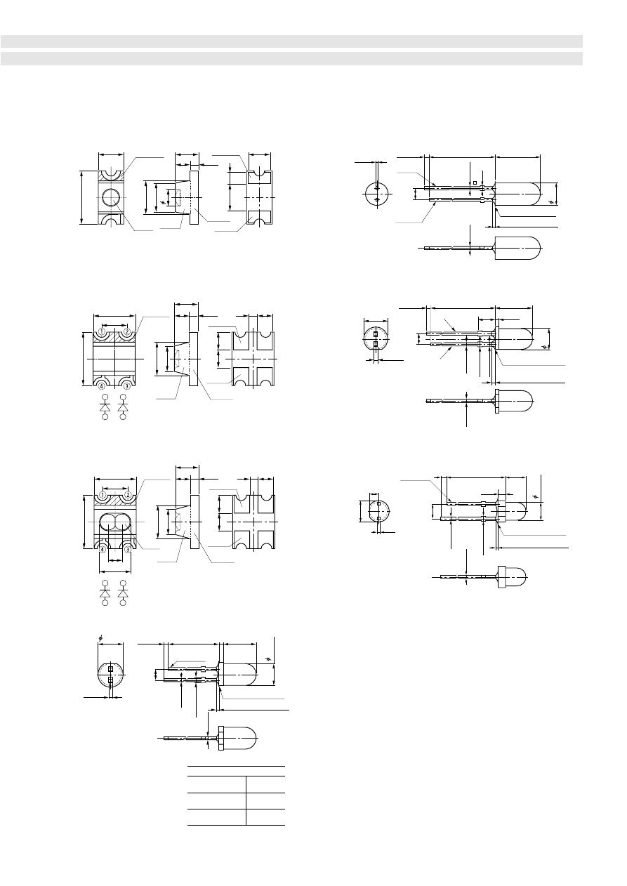
129
Fig. 41
Fig. 42
Fig. 43
Fig. 44
Fig. 45
Fig. 46
Fig. 47
0.5
±
0.1
Anode
Cathode
1.0min
21.0min
9.4
±
0.3
5.0
±
0.2
Resin heap 0.8max
Resin burr 0.3max
0.65
max
0.5
±
0.1
0.5
±
0.1
(2.54)
1.7
ø
3.8
0.4
1.0min
25.8min
3.5
±
0.1
(1.3)
0.45
±
0.1
0.65max
Resin burr 0.3max
Resin heap 1.5max
3.1
±
0.1
Cathode
(2.54)
0.4
±
0.1
5.6
±
0.2
23.0min
1.0min
A
Cathode
0.65max
Resin heap 1.5max
Resin burr 0.3max
5.0
±
0.2
0.5
±
0.1
0.5
±
0.1
(1.0)
(2.54)
0.5
±
0.1
5.6
24.0min
8.5
±
0.5
Anode
(2.54)
0.6
±
0.1
1.1max
0.85
+0.1
Resin heap 1.5max
0.6
±
0.1
0.6
±
0.1
Resin burr 0.3max
4.8
±
0.2
Cathode
2.0min
(0.8)
A
2.5
1.5
3.0
2.0
1.5
1.4
±
0.1
1.0
1.0
0.9
0.6
±
0.1
P.C.B.
Anode
Cathode
Cathode
mark
0.9
(0.5)
Resin
1.5
3.0
2.0
1.7
1.4
(0.5)
0.9
1.6
0
.6
1.3
Lens
Resin
Anode
Cathode
Cathode
mark
P.C.B.
1.0
2.5
1.5
0.8
1.8
3.0
2.0
1.5
1.4
±
0.1
1.0
1.0
0.9
0.6
±
0.1
Lens
P.C.B.
Anode
Cathode
Cathode
mark
0.9
(0.5)
Resin
Dimension A (mm)
SID303C
3.0
±
0.5
3.6
±
0.5
4.2
±
0.5
SID313BP
SID1003BQ
SID307BR
SID1G307C
(Unit: mm)
A
B
3
4
1
2
A
B
3
4
1
2
General-purpose LEDs - External Dimensions

Power transistor
Power transistor
Power transistor
Power transistor
Power transistor
Power transistor
Power transistor
Power transistor
Power transistor
Power transistor
Power transistor
Power transistor
MOS FET
Hall-Effect IC (Unipolar Switch)
Hall-Effect IC (Unipolar Switch)
Hall-Effect IC (Unipolar Switch)
Hall-Effect IC (Bipolar Switch)
Hall-Effect IC (Unipolar Switch)
Hall-Effect IC (Unipolar Switch)
Hall-Effect IC (Unipolar Switch)
Hall-Effect IC (Unipolar Switch)
Hall-Effect IC (Bipolar Latch)
Hall-Effect IC (Bipolar Latch)
Hall-Effect IC (Bipolar Latch)
Hall-Effect IC (Bipolar Latch)
Hall-Effect IC (Unipolar Switch)
Hall-Effect IC (Unipolar Switch)
Hall-Effect IC (Bipolar Latch)
Hall-Effect IC (Bipolar Latch)
Hall-Effect IC (Bipolar Latch)
Hall-Effect IC (Linear Sensor)
Hall-Effect IC (Linear Sensor)
Ultra-Fast-Recovery Rectifier Diode (Axial)
Ultra-Fast-Recovery Rectifier Diode (Axial)
Ultra-Fast-Recovery Rectifier Diode (Axial)
Ultra-Fast-Recovery Rectifier Diode (Axial)
Schottky barrier Diode (Axial)
Schottky barrier Diode (Axial)
Schottky barrier Diode (Axial)
Schottky barrier Diode (Axial)
Ultra-Fast-Recovery Rectifier Diode (Axial)
Rectifier Diode (Axial)
Rectifier Diode (Axial)
Rectifier Diode (Axial)
Ultra-Fast-Recovery Rectifier Diode (Axial)
Fast-Recovery Rectifier Diode (Axial)
Fast-Recovery Rectifier Diode (Axial)
Fast-Recovery Rectifier Diode (Axial)
Hall-Effect IC (Subassembly)
Part No.
Classification
Page
Part No.
Classification
Page
Part No.
Classification
Page
2SA1488
2SA1488A
2SA1567
2SA1568
2SC3851
2SC3852
2SC4024
2SC4065
2SC4153
2SD2141
2SD2382
2SD2633
2SK2701
A3121L*
A3122L*
A3123L*
A3134L*
A3141L*
A3142L*
A3143L*
A3144L*
A3185L*
A3187L*
A3188L*
A3189L*
A3240L*
A3250L*
A3280L*
A3281L*
A3283L*
A3515LUA
A3516LUA
AG01
AG01A
AG01Y
AG01Z
AK 03
AK 04
AK 06
AK 09
AL01Z
AM01
AM01A
AM01Z
AP01C
AS01
AS01A
AS01Z
ATS610LSA
66
66
67
68
69
70
71
72
73
74
75
76
92
60
60
60
60
60
60
60
60
60
60
60
60
60
60
60
60
60
60
60
112
112
112
112
113
113
113
113
112
110
110
110
112
111
111
111
60
Hall-Effect IC (Subassembly)
Hall-Effect IC (Subassembly)
Fast-Recovery Rectifier Diode (Axial)
Fast-Recovery Rectifier Diode (Axial)
Fast-Recovery Rectifier Diode (Axial)
Fast-Recovery Rectifier Diode (Axial)
Ultra-Fast-Recovery Rectifier Diode (Axial)
Ultra-Fast-Recovery Rectifier Diode (Axial)
Ultra-Fast-Recovery Rectifier Diode (Axial)
Ultra-Fast-Recovery Rectifier Diode (Axial)
Ultra-Fast-Recovery Rectifier Diode (Axial)
Ultra-Fast-Recovery Rectifier Diode (Axial)
Ultra-Fast-Recovery Rectifier Diode (Axial)
Ultra-Fast-Recovery Rectifier Diode (Axial)
Ultra-Fast-Recovery Rectifier Diode (Axial)
Fast-Recovery Rectifier Diode (Axial)
Fast-Recovery Rectifier Diode (Axial)
Fast-Recovery Rectifier Diode (Axial)
Schottky barrier Diode (Axial)
Schottky barrier Diode (Axial)
Schottky barrier Diode (Axial)
Schottky barrier Diode (Axial)
Schottky barrier Diode (Axial)
Schottky barrier Diode (Axial)
Schottky barrier Diode (Axial)
Schottky barrier Diode (Axial)
Ultra-Fast-Recovery Rectifier Diode (Axial)
Ultra-Fast-Recovery Rectifier Diode (Axial)
Ultra-Fast-Recovery Rectifier Diode (Axial)
Rectifier Diode (Axial)
Rectifier Diode (Axial)
Rectifier Diode (Axial)
Rectifier Diode (Axial)
Rectifier Diode (Axial)
Rectifier Diode (Axial)
Rectifier Diode (Axial)
Rectifier Diode (Axial)
Rectifier Diode (Axial)
Rectifier Diode (Axial)
Rectifier Diode (Axial)
Rectifier Diode (Axial)
Ultra-Fast-Recovery Rectifier Diode (Axial)
Ultra-Fast-Recovery Rectifier Diode (Axial)
Fast-Recovery Rectifier Diode (Axial)
Fast-Recovery Rectifier Diode (Axial)
Fast-Recovery Rectifier Diode (Axial)
Fast-Recovery Rectifier Diode (Axial)
Fast-Recovery Rectifier Diode (Axial)
Fast-Recovery Rectifier Diode (Axial)
ATS611LSB
ATS612LSB
AU01
AU01Z
AU02
AU02Z
EG 1
EG 1A
EG 1Y
EG 1Z
EG01
EG01A
EG01C
EG01Y
EG01Z
EH 1
EH 1A
EH 1Z
EK 03
EK 04
EK 06
EK 09
EK 13
EK 14
EK 16
EK 19
EL 1
EL 1Z
EL02Z
EM 1
EM 1A
EM 1B
EM 1C
EM 1Y
EM 1Z
EM 2
EM 2A
EM 2B
EM01
EM01A
EM01Z
EN 01Z
EP01C
ES 1
ES 1A
ES 1F
ES 1Z
ES01
ES01A
60
60
111
111
111
111
112
112
112
112
112
112
112
112
112
111
111
111
113
113
113
113
113
113
113
113
112
112
112
110
110
110
110
110
110
110
110
110
110
110
110
112
112
111
111
111
111
111
111
Fast-Recovery Rectifier Diode (Axial)
Fast-Recovery Rectifier Diode (Axial)
Fast-Recovery Rectifier Diode (Axial)
Fast-Recovery Rectifier Diode (Axial)
Fast-Recovery Rectifier Diode (Axial)
Fast-Recovery Rectifier Diode (Axial)
Fast-Recovery Rectifier Diode (Axial)
Fast-Recovery Rectifier Diode (Axial)
Fast-Recovery Rectifier Diode (Axial)
Fast-Recovery Rectifier Diode (Axial)
Fast-Recovery Rectifier Diode (Axial)
Fast-Recovery Rectifier Diode (Axial)
Fast-Recovery Rectifier Diode (Axial)
Fast-Recovery Rectifier Diode (Axial)
Fast-Recovery Rectifier Diode (Axial)
MOS FET
MOS FET
MOS FET
MOS FET
MOS FET
MOS FET
Schottky barrier Diode (Center-tap)
Schottky barrier Diode (Center-tap)
Schottky barrier Diode (Center-tap)
Schottky barrier Diode (Center-tap)
Schottky barrier Diode (Center-tap)
Schottky barrier Diode (Center-tap)
Schottky barrier Diode (Center-tap)
Schottky barrier Diode (Center-tap)
Schottky barrier Diode (Center-tap)
Schottky barrier Diode (Center-tap)
Schottky barrier Diode (Center-tap)
Schottky barrier Diode (Center-tap)
Schottky barrier Diode (Center-tap)
Schottky barrier Diode (Center-tap)
Schottky barrier Diode (Center-tap)
Schottky barrier Diode (Frame 2-pin)
Schottky barrier Diode (Frame 2-pin)
Schottky barrier Diode (Frame 2-pin)
Schottky barrier Diode (Frame 2-pin)
Schottky barrier Diode (Frame 2-pin)
Ultra-Fast-Recovery Rectifier Diode (Frame 2-pin)
Schottky barrier Diode (Center-tap)
Schottky barrier Diode (Center-tap)
Ultra-Fast-Recovery Rectifier Diode (Center-tap)
Ultra-Fast-Recovery Rectifier Diode (Center-tap)
Ultra-Fast-Recovery Rectifier Diode (Center-tap)
Ultra-Fast-Recovery Rectifier Diode (Center-tap)
Ultra-Fast-Recovery Rectifier Diode (Center-tap)
ES01F
ES01Z
EU 1
EU 1A
EU 1Z
EU 2
EU 2A
EU 2YX
EU 2Z
EU01
EU01A
EU01Z
EU02
EU02A
EU02Z
FKV460
FKV460S
FKV560
FKV560S
FKV660
FKV660S
FMB-24
FMB-24H
FMB-24L
FMB-24M
FMB-26
FMB-26L
FMB-29
FMB-29L
FMB-34
FMB-34M
FMB-34S
FMB-36
FMB-36M
FMB-39
FMB-39M
FMB-G14
FMB-G14L
FMB-G16L
FMB-G19L
FMB-G24H
FMD-G26S
FME-24H
FME-24L
FMG-12S,R
FMG-13S,R
FMG-14S,R
FMG-22S,R
FMG-23S,R
111
111
111
111
111
111
111
111
111
111
111
111
111
111
111
93
94
95
96
97
98
113
113
113
113
113
113
113
113
113
113
113
113
113
113
113
113
113
113
113
113
112
113
113
112
112
112
112
112
Index by Part No.
130

131
Ultra-Fast-Recovery Rectifier Diode (Center-tap)
Ultra-Fast-Recovery Rectifier Diode (Center-tap)
Ultra-Fast-Recovery Rectifier Diode (Center-tap)
Ultra-Fast-Recovery Rectifier Diode (Center-tap)
Ultra-Fast-Recovery Rectifier Diode (Center-tap)
Ultra-Fast-Recovery Rectifier Diode (Center-tap)
Ultra-Fast-Recovery Rectifier Diode (Frame 2-pin)
Ultra-Fast-Recovery Rectifier Diode (Frame 2-pin)
Ultra-Fast-Recovery Rectifier Diode (Frame 2-pin)
Ultra-Fast-Recovery Rectifier Diode (Frame 2-pin)
Ultra-Fast-Recovery Rectifier Diode (Center-tap)
Ultra-Fast-Recovery Rectifier Diode (Center-tap)
Ultra-Fast-Recovery Rectifier Diode (Center-tap)
Ultra-Fast-Recovery Rectifier Diode (Center-tap)
Ultra-Fast-Recovery Rectifier Diode (Center-tap)
Ultra-Fast-Recovery Rectifier Diode (Center-tap)
Ultra-Fast-Recovery Rectifier Diode (Center-tap)
Ultra-Fast-Recovery Rectifier Diode (Center-tap)
Ultra-Fast-Recovery Rectifier Diode (Center-tap)
Ultra-Fast-Recovery Rectifier Diode (Center-tap)
Ultra-Fast-Recovery Rectifier Diode (Frame 2-pin)
Ultra-Fast-Recovery Rectifier Diode (Frame 2-pin)
Ultra-Fast-Recovery Rectifier Diode (Frame 2-pin)
Ultra-Fast-Recovery Rectifier Diode (Frame 2-pin)
Ultra-Fast-Recovery Rectifier Diode (Frame 2-pin)
Ultra-Fast-Recovery Rectifier Diode (Frame 2-pin)
Rectifier Diode (Center-tap)
Rectifier Diode (Center-tap)
Rectifier Diode (Center-tap)
Rectifier Diode (Center-tap)
Rectifier Diode (Center-tap)
Rectifier Diode (Center-tap)
Rectifier Diode (Center-tap)
Ultra-Fast-Recovery Rectifier Diode (Frame 2-pin)
Ultra-Fast-Recovery Rectifier Diode (Frame 2-pin)
Ultra-Fast-Recovery Rectifier Diode (Frame 2-pin)
Ultra-Fast-Recovery Rectifier Diode (Frame 2-pin)
Fast-Recovery Rectifier Diode (Center-tap)
Fast-Recovery Rectifier Diode (Center-tap)
Fast-Recovery Rectifier Diode (Center-tap)
Fast-Recovery Rectifier Diode (Center-tap)
Fast-Recovery Rectifier Diode (Center-tap)
Fast-Recovery Rectifier Diode (Center-tap)
Fast-Recovery Rectifier Diode (Center-tap)
Fast-Recovery Rectifier Diode (Frame 2-pin)
Power transistor
Power transistor
Power transistor
Power transistor
FMG-24S,R
FMG-26S,R
FMG-32S,R
FMG-33S,R
FMG-34S,R
FMG-36S,R
FMG-G26S
FMG-G2CS
FMG-G36S
FMG-G3CS
FML-12S
FML-13S
FML-14S
FML-22S
FML-23S
FML-24S
FML-32S
FML-33S
FML-34S
FML-36S
FML-G12S
FML-G13S
FML-G14S
FML-G16S
FML-G22S
FML-G26S
FMM-22S,R
FMM-24S,R
FMM-26S,R
FMM-31S,R
FMM-32S,R
FMM-34S,R
FMM-36S,R
FMN-G12S
FMN-G14S
FMN-G16S
FMP-G12S
FMU-12S,R
FMU-14S,R
FMU-21S,R
FMU-22S,R
FMU-24S,R
FMU-32S,R
FMU-34S,R
FMU-G2YXS
FN812
FP812
MN611S
MN638S
Schottky barrier Diode (Center-tap)
Power Zener Diode (Axial)
Schottky barrier Diode (Bridge)
Ultra-Fast-Recovery Rectifier Diode (Bridge)
Fast-Recovery Rectifier Diode (Axial)
Fast-Recovery Rectifier Diode (Axial)
Fast-Recovery Rectifier Diode (Axial)
Fast-Recovery Rectifier Diode (Axial)
Fast-Recovery Rectifier Diode (Axial)
Ultra-Fast-Recovery Rectifier Diode (Axial)
Ultra-Fast-Recovery Rectifier Diode (Axial)
Ultra-Fast-Recovery Rectifier Diode (Axial)
Ultra-Fast-Recovery Rectifier Diode (Axial)
Ultra-Fast-Recovery Rectifier Diode (Axial)
Ultra-Fast-Recovery Rectifier Diode (Axial)
Ultra-Fast-Recovery Rectifier Diode (Axial)
Ultra-Fast-Recovery Rectifier Diode (Axial)
Ultra-Fast-Recovery Rectifier Diode (Axial)
Ultra-Fast-Recovery Rectifier Diode (Axial)
Ultra-Fast-Recovery Rectifier Diode (Axial)
Ultra-Fast-Recovery Rectifier Diode (Axial)
Ultra-Fast-Recovery Rectifier Diode (Axial)
Ultra-Fast-Recovery Rectifier Diode (Axial)
Fast-Recovery Rectifier Diode (Axial)
Fast-Recovery Rectifier Diode (Axial)
Fast-Recovery Rectifier Diode (Axial)
Fast-Recovery Rectifier Diode (Axial)
Fast-Recovery Rectifier Diode (Axial)
Schottky barrier Diode (Axial)
Schottky barrier Diode (Axial)
Schottky barrier Diode (Axial)
Schottky barrier Diode (Axial)
Schottky barrier Diode (Axial)
Schottky barrier Diode (Axial)
Schottky barrier Diode (Axial)
Schottky barrier Diode (Axial)
Schottky barrier Diode (Axial)
Schottky barrier Diode (Axial)
Schottky barrier Diode (Axial)
Schottky barrier Diode (Axial)
Schottky barrier Diode (Axial)
Ultra-Fast-Recovery Rectifier Diode (Axial)
Ultra-Fast-Recovery Rectifier Diode (Axial)
Ultra-Fast-Recovery Rectifier Diode (Axial)
Ultra-Fast-Recovery Rectifier Diode (Axial)
Ultra-Fast-Recovery Rectifier Diode (Axial)
Ultra-Fast-Recovery Rectifier Diode (Axial)
Ultra-Fast-Recovery Rectifier Diode (Axial)
Ultra-Fast-Recovery Rectifier Diode (Axial)
MPE-24H
PZ 628
RBV-406B
RBV-602L
RC 2
RF 1
RF 1A
RF 1B
RF 1Z
RG 10
RG 10A
RG 10Y
RG 10Z
RG 1C
RG 2
RG 2A
RG 2Y
RG 2Z
RG 4
RG 4A
RG 4C
RG 4Y
RG 4Z
RH 1
RH 1A
RH 1B
RH 1C
RH 1Z
RJ 43
RK 13
RK 14
RK 16
RK 19
RK 33
RK 34
RK 36
RK 39
RK 43
RK 44
RK 46
RK 49
RL 10Z
RL 2
RL 2A
RL 2Z
RL 3
RL 3A
RL 3Z
RL 4A
113
109
113
112
111
111
111
111
111
112
112
112
112
112
112
112
112
112
112
112
112
112
112
111
111
111
111
111
113
113
113
113
113
113
113
113
113
113
113
113
113
112
112
112
112
112
112
112
112
112
112
112
112
112
112
112
112
112
112
112
112
112
112
112
112
112
112
112
112
112
112
112
112
112
112
110
110
110
110
110
110
110
112
112
112
112
111
111
111
111
111
111
111
111
77
78
79
80
Ultra-Fast-Recovery Rectifier Diode (Axial)
Rectifier Diode (Axial)
Rectifier Diode (Axial)
Rectifier Diode (Axial)
Rectifier Diode (Axial)
Rectifier Diode (Axial)
Rectifier Diode (Axial)
Rectifier Diode (Axial)
Rectifier Diode (Axial)
Rectifier Diode (Axial)
Rectifier Diode (Axial)
Rectifier Diode (Axial)
Rectifier Diode (Axial)
Rectifier Diode (Axial)
Rectifier Diode (Axial)
Rectifier Diode (Axial)
Rectifier Diode (Axial)
Rectifier Diode (Axial)
Rectifier Diode (Axial)
Rectifier Diode (Axial)
Rectifier Diode (Axial)
Rectifier Diode (Axial)
Rectifier Diode (Axial)
Rectifier Diode (Axial)
Rectifier Diode (Axial)
Rectifier Diode (Axial)
Rectifier Diode (Axial)
Rectifier Diode (Axial)
Rectifier Diode (Axial)
Ultra-Fast-Recovery Rectifier Diode (Axial)
Ultra-Fast-Recovery Rectifier Diode (Axial)
Ultra-Fast-Recovery Rectifier Diode (Axial)
Ultra-Fast-Recovery Rectifier Diode (Axial)
Rectifier Diode (Axial)
Rectifier Diode (Axial)
Rectifier Diode (Axial)
Rectifier Diode (Axial)
Rectifier Diode (Axial)
Ultra-Fast-Recovery Rectifier Diode (Axial)
Fast-Recovery Rectifier Diode (Axial)
Fast-Recovery Rectifier Diode (Axial)
Fast-Recovery Rectifier Diode (Axial)
Fast-Recovery Rectifier Diode (Axial)
Fast-Recovery Rectifier Diode (Axial)
Fast-Recovery Rectifier Diode (Axial)
Ultra-Fast-Recovery Rectifier Diode (Axial)
Fast-Recovery Rectifier Diode (Axial)
Fast-Recovery Rectifier Diode (Axial)
Fast-Recovery Rectifier Diode (Axial)
RL 4Z
RM 1
RM 10
RM 10A
RM 10B
RM 10Z
RM 11A
RM 11B
RM 11C
RM 1A
RM 1B
RM 1C
RM 1Z
RM 2
RM 2A
RM 2B
RM 2C
RM 2Z
RM 3
RM 3A
RM 3B
RM 3C
RM 4
RM 4A
RM 4AM
RM 4B
RM 4C
RM 4Y
RM 4Z
RN 1Z
RN 2Z
RN 3Z
RN 4Z
RO 2
RO 2A
RO 2B
RO 2C
RO 2Z
RP 1H
RS 1A
RS 1B
RU 1
RU 1A
RU 1B
RU 1C
RU 1P
RU 2
RU 20A
RU 2AM
112
110
110
110
110
110
110
110
110
110
110
110
110
110
110
110
110
110
110
110
110
110
110
110
110
110
110
110
110
112
112
112
112
110
110
110
110
110
112
111
111
111
111
111
111
112
111
111
111
Part No.
Classification
Page
Part No.
Classification
Page
Part No.
Classification
Page
Index by Part No.

Fast-Recovery Rectifier Diode (Axial)
Fast-Recovery Rectifier Diode (Axial)
Fast-Recovery Rectifier Diode (Axial)
Fast-Recovery Rectifier Diode (Axial)
Fast-Recovery Rectifier Diode (Axial)
Fast-Recovery Rectifier Diode (Axial)
Fast-Recovery Rectifier Diode (Axial)
Fast-Recovery Rectifier Diode (Axial)
Fast-Recovery Rectifier Diode (Axial)
Fast-Recovery Rectifier Diode (Axial)
Fast-Recovery Rectifier Diode (Axial)
Fast-Recovery Rectifier Diode (Axial)
Fast-Recovery Rectifier Diode (Axial)
Fast-Recovery Rectifier Diode (Axial)
Fast-Recovery Rectifier Diode (Axial)
Fast-Recovery Rectifier Diode (Axial)
Fast-Recovery Rectifier Diode (Axial)
Fast-Recovery Rectifier Diode (Axial)
Fast-Recovery Rectifier Diode (Axial)
Fast-Recovery Rectifier Diode (Axial)
Fast-Recovery Rectifier Diode (Axial)
Fast-Recovery Rectifier Diode (Axial)
Fast-Recovery Rectifier Diode (Axial)
Fast-Recovery Rectifier Diode (Axial)
Fast-Recovery Rectifier Diode (Axial)
Fast-Recovery Rectifier Diode (Axial)
Fast-Recovery Rectifier Diode (Axial)
Power transistor Array (Surface Mount)
Power transistor Array (Surface Mount)
Power transistor Array (Surface Mount)
High-side Power Switch IC (Surface Mount 2-circuits)
MOS FET Array (Surface mount)
MOS FET Array (Surface mount)
MOS FET Array (Surface mount)
Flat Lens Deep Red Chip LED
Flat Lens Red Chip LED
Inner Lens Red Chip LED
Flat Lens Green Chip LED
Flat Lens Deep Green Chip LED
Inner Lens Green Chip LED
Inner Lens Deep Green Chip LED
Flat Lens Pure Green Chip LED
Inner Lens Pure Green Chip LED
Flat Lens GaAlAs Red Chip LED
Inner Lens GaAlAs Red Chip LED
Flat Lens Yellow Chip LED
Inner Lens Yellow Chip LED
Flat Lens Amber Chip LED
Inner Lens Amber Chip LED
RU 2B
RU 2C
RU 2M
RU 2YX
RU 2Z
RU 3
RU 30
RU 30A
RU 30Y
RU 30Z
RU 31
RU 31A
RU 3A
RU 3AM
RU 3B
RU 3C
RU 3M
RU 3YX
RU 4
RU 4A
RU 4AM
RU 4B
RU 4C
RU 4M
RU 4Y
RU 4YX
RU 4Z
SDA03
SDA04
SDC09
SDH04
SDK06
SDK08
SDK09
SEC1101C
SEC1201C
SEC1203C
SEC1401C
SEC1401E-TG
SEC1403C
SEC1403E-TG
SEC1501C
SEC1503C
SEC1601C
SEC1603C
SEC1701C-YG
SEC1703C
SEC1801C
SEC1803C
111
111
111
111
111
111
111
111
111
111
111
111
111
111
111
111
111
111
111
111
111
111
111
111
111
111
111
88
89
90
26
103
104
105
123
123
123
123
123
123
123
123
123
123
123
123
123
123
123
Flat Lens Orange Chip LED
Inner Lens Orange Chip LED
Flat Lens GaN Blue Chip LED
Flat Lens Green / Red Bicolor Chip LED
Inner Lens Green / Red Bicolor Chip LED
Flat Lens Green / GaAlAs Red Bicolor Chip LED
Inner Lens Green / Amber Bicolor Chip LED
Flat Lens Green / Orange Bicolor Chip LED
Inner Lens Green / Orange Bicolor Chip LED
Flat Lens Green / Green Chip LED
Inner Lens Green / Green Chip LED
Flat Lens Pure Green / Orange Bicolor Chip LED
Flat Lens Yellow / GaAlAs Red Bicolor Chip LED
Inner Lens Yellow / GaAlAs Red Bicolor Chip LED
Inner Lens Yellow / Yellow Chip LED
Flat Lens AlGaInP Red Chip LED
Flat Lens InGaN Pure Green Chip LED
Flat Lens InGaN Blue Chip LED
5ø Round Deep Red LED Lamp
5ø Round Deep Red LED Lamp
5ø Round Deep Red LED Lamp
5ø Round Cylindrical Deep Red LED Lamp
2
✕
5 Rectangular Deep Red LED Lamp
3
✕
5 Rectangular Deep Red LED Lamp
1
✕
5 Rectangular Deep Red LED Lamp
5ø Round Red LED Lamp
5ø Round Red LED Lamp
5ø Round Red LED Lamp
5ø Round Red LED Lamp
5ø Round Cylindrical Red LED Lamp
For Surface Illumination Red LED Lamp
2
✕
5 Rectangular Red LED Lamp
2.5
✕
5 Rectangular Red LED Lamp
5ø Round Red LED Lamp
5ø Round Red LED Lamp
5ø Round Green LED Lamp
5ø Round Green LED Lamp
5ø Round Green LED Lamp
5ø Round Green LED Lamp
5ø Round Cylindrical Green LED Lamp
For Surface Illumination Green LED Lamp
2
✕
5 Rectangular Green LED Lamp
3
✕
5 Rectangular Green LED Lamp
2.5
✕
5 Rectangular Green LED Lamp
1
✕
5 Rectangular Green LED Lamp
5ø Round Green LED Lamp
5ø Round Green LED Lamp
4.6
✕
5.6ø Egg-shaped Green LED Lamp
5ø Round Pure Green LED Lamp
SEC1901C
SEC1903C
SEC1E01C
SEC2422C
SEC2442C
SEC2462C
SEC2484C
SEC2492C
SEC2494C
SEC2552C
SEC2554C
SEC2592C
SEC2762C-YG
SEC2764C
SEC2774C
SECS1203C
SECU1D01C
SECU1E01C
SEL1110R
SEL1110S
SEL1110W
SEL1111R
SEL1120R
SEL1121R
SEL1124R
SEL1210R
SEL1210RM
SEL1210S
SEL1210SM
SEL1211R
SEL1213C
SEL1220R
SEL1222R
SEL1250RM
SEL1250SM
SEL1410E
SEL1410EM
SEL1410G
SEL1410GM
SEL1411G
SEL1413E
SEL1420G
SEL1421G
SEL1422G
SEL1424G
SEL1450EKM
SEL1450GM-YG
SEL1453CEMKT
SEL1510C
123
123
123
123
123
123
123
123
123
123
123
123
123
123
123
123
123
123
119
119
119
119
121
120
121
119
119
119
119
119
120
121
121
119
119
119
119
119
119
119
120
121
120
121
121
119
119
119
119
5ø Round Pure Green LED Lamp
For Surface Illumination Pure Green LED Lamp
5ø Round Pure Green LED Lamp
5ø Round GaAlAs Red LED Lamp
5ø Round GaAlAs Red LED Lamp
5ø Round GaAlAs Red LED Lamp
5ø Round Yellow LED Lamp
5ø Round Yellow LED Lamp
5ø Round Yellow LED Lamp
5ø Round Cylindrical Yellow LED Lamp
For Surface Illumination Yellow LED Lamp
2
✕
5 Rectangular Yellow LED Lamp
3
✕
5 Rectangular Yellow LED Lamp
2.5
✕
5 Rectangular Yellow LED Lamp
2.5
✕
5 Rectangular Yellow LED Lamp
1
✕
5 Rectangular Yellow LED Lamp
5ø Round Amber LED Lamp
5ø Round Amber LED Lamp
5ø Round Amber LED Lamp
5ø Round Amber LED Lamp
5ø Round Cylindrical Amber LED Lamp
For Surface Illumination Amber LED Lamp
2
✕
5 Rectangular Amber LED Lamp
3
✕
5 Rectangular Amber LED Lamp
2.5
✕
5 Rectangular Amber LED Lamp
1
✕
5 Rectangular Amber LED Lamp
5ø Round Amber LED Lamp
5ø Round Amber LED Lamp
5ø Round Orange LED Lamp
5ø Round Orange LED Lamp
5ø Round Orange LED Lamp
5ø Round Orange LED Lamp
5ø Round Cylindrical Orange LED Lamp
For Surface Illumination Orange LED Lamp
2
✕
5 Rectangular Orange LED Lamp
3
✕
5 Rectangular Orange LED Lamp
2.5
✕
5 Rectangular Orange LED Lamp
1
✕
5 Rectangular Orange LED Lamp
5ø Round Orange LED Lamp
3ø Round Deep Red LED Lamp
3ø Round Deep Red LED Lamp
3ø Round Deep Red LED Lamp
3ø Round Cylindrical Deep Red LED Lamp
3ø Round Red LED Lamp
3ø Round Red LED Lamp
3ø Round Red LED Lamp
For Surface Illumination Red LED Lamp
3ø Round Red LED Lamp
3ø Round Red LED Lamp
SEL1510CM
SEL1513E
SEL1550CM
SEL1610C
SEL1610W
SEL1615C
SEL1710K
SEL1710KM
SEL1710Y
SEL1711Y
SEL1713K
SEL1720Y
SEL1721Y
SEL1722K
SEL1722Y
SEL1724Y
SEL1810A
SEL1810AM
SEL1810D
SEL1810DM
SEL1811D
SEL1813A
SEL1820D
SEL1821D
SEL1822D
SEL1824D
SEL1850AM
SEL1850DM
SEL1910A
SEL1910AM
SEL1910D
SEL1910DM
SEL1911D
SEL1913K
SEL1920D
SEL1921D
SEL1922D
SEL1924D
SEL1950KM
SEL2110R
SEL2110S
SEL2110W
SEL2111R
SEL2210R
SEL2210S
SEL2210W
SEL2213C
SEL2215R
SEL2215S
119
120
119
119
119
119
119
119
119
119
120
121
120
121
121
121
119
119
119
119
119
120
121
120
121
121
119
119
119
119
119
119
119
120
121
120
121
121
119
120
120
120
120
120
120
120
120
120
120
132
Part No.
Classification
Page
Part No.
Classification
Page
Part No.
Classification
Page
Index by Part No.

133
3ø Round Green LED Lamp
3ø Round Green LED Lamp
3ø Round Cylindrical Green LED Lamp
For Surface Illumination Green LED Lamp
For Surface Illumination Green LED Lamp
3ø Round Green LED Lamp
3ø Round Green LED Lamp
3ø Round Pure Green LED Lamp
3ø Round Pure Green LED Lamp
For Surface Illumination Pure Green LED Lamp
3ø Round Pure Green LED Lamp
3ø Round GaAlAs Red LED Lamp
For Surface Illumination GaAlAs Red LED Lamp
3ø Round Yellow LED Lamp
3ø Round Yellow LED Lamp
For Surface Illumination Yellow LED Lamp
3ø Round Yellow LED Lamp
3ø Round Yellow LED Lamp
3ø Round Amber LED Lamp
3ø Round Amber LED Lamp
For Surface Illumination Amber LED Lamp
3ø Round Amber LED Lamp
3ø Round Amber LED Lamp
3ø Round Orange LED Lamp
3ø Round Orange LED Lamp
3ø Round Cylindrical Orange LED Lamp
For Surface Illumination Orange LED Lamp
3ø Round Orange LED Lamp
3ø Round Orange LED Lamp
3ø Round GaN Blue LED Lamp
4ø Round Deep Red LED Lamp
4ø Round Deep Red LED Lamp
4ø Round Deep Red LED Lamp
4ø Round Deep Red LED Lamp
2ø Round Deep Red LED Lamp
4ø Round Red LED Lamp
4ø Round Red LED Lamp
4ø Round Red LED Lamp
4ø Round Red LED Lamp
2
✕
4 Rectangular Red LED Lamp
2
✕
4 Rectangular Red LED Lamp
2
✕
4 Rectangular Red LED Lamp
2
✕
4 Rectangular Red LED Lamp
4ø Bow-shaped Red LED Lamp
3.1ø Bow-shaped Red LED Lamp
3.1ø Bow-shaped Red LED Lamp
4ø Round Green LED Lamp
4ø Round Green LED Lamp
4ø Round Green LED Lamp
SEL2410E
SEL2410G
SEL2411G
SEL2413E
SEL2413G
SEL2415E
SEL2415G
SEL2510C
SEL2510G
SEL2513E
SEL2515C
SEL2610C
SEL2613CS-S
SEL2710K
SEL2710Y
SEL2713K
SEL2715K
SEL2715Y
SEL2810A
SEL2810D
SEL2813A
SEL2815A
SEL2815D
SEL2910A
SEL2910D
SEL2911D
SEL2913K
SEL2915A
SEL2915D
SEL2E10C
SEL4110R
SEL4110S
SEL4114R
SEL4114S
SEL4117R
SEL4210R
SEL4210S
SEL4214R
SEL4214S
SEL4225C
SEL4225R
SEL4226C
SEL4226R
SEL4227C
SEL4228C
SEL4229R
SEL4410E
SEL4410G
SEL4414E
120
120
120
120
120
120
120
120
120
120
120
120
120
120
120
120
120
120
120
120
120
120
120
120
120
120
120
120
120
120
119
119
119
119
120
119
119
119
119
121
121
121
121
121
121
121
119
119
119
4ø Round Green LED Lamp
2ø Round Green LED Lamp
2
✕
4 Rectangular Green LED Lamp
2
✕
4 Rectangular Green LED Lamp
2
✕
4 Rectangular Green LED Lamp
2
✕
4 Rectangular Green LED Lamp
4ø Bow-shaped Green LED Lamp
3.1ø Bow-shaped Deep Green LED Lamp
3.1ø Bow-shaped Green LED Lamp
3.1ø Bow-shaped Green LED Lamp
4ø Round Pure Green LED Lamp
4ø Round Pure Green LED Lamp
2
✕
4 Rectangular Pure Green LED Lamp
3.1ø Bow-shaped Pure Green LED Lamp
3.1ø Bow-shaped GaAlAs Red LED Lamp
4ø Round Yellow LED Lamp
4ø Round Yellow LED Lamp
4ø Round Yellow LED Lamp
4ø Round Yellow LED Lamp
2ø Round Yellow LED Lamp
2
✕
4 Rectangular Yellow LED Lamp
2
✕
4 Rectangular Yellow LED Lamp
2
✕
4 Rectangular Yellow LED Lamp
2
✕
4 Rectangular Yellow LED Lamp
3.1ø Bow-shaped Yellow LED Lamp
3.1ø Bow-shaped Yellow LED Lamp
4ø Round amber LED Lamp
4ø Round amber LED Lamp
4ø Round amber LED Lamp
4ø Round amber LED Lamp
2ø Round Amber LED Lamp
2
✕
4 Rectangular Amber LED Lamp
2
✕
4 Rectangular Amber LED Lamp
2
✕
4 Rectangular Amber LED Lamp
2
✕
4 Rectangular Amber LED Lamp
3.1ø Bow-shaped Amber LED Lamp
3.1ø Bow-shaped Amber LED Lamp
4ø Round Orange LED Lamp
4ø Round Orange LED Lamp
4ø Round Orange LED Lamp
4ø Round Orange LED Lamp
2ø Round Orange LED Lamp
2
✕
4 Rectangular Orange LED Lamp
2
✕
4 Rectangular Orange LED Lamp
2
✕
4 Rectangular Orange LED Lamp
2
✕
4 Rectangular Orange LED Lamp
3.1ø Bow-shaped Orange LED Lamp
3.1ø Bow-shaped Orange LED Lamp
5mm Pitch Lead Rectangular Red LED Lamp
SEL4414G
SEL4417G
SEL4425E
SEL4425G
SEL4426E
SEL4426G
SEL4427EP
SEL4428B-TG
SEL4428E
SEL4429E
SEL4510C
SEL4514C
SEL4525C
SEL4528C
SEL4628C-S
SEL4710K
SEL4710Y
SEL4714K
SEL4714Y
SEL4717Y
SEL4725K
SEL4725Y
SEL4726K
SEL4726Y
SEL4728K
SEL4729KH
SEL4810A
SEL4810D
SEL4814A
SEL4814D
SEL4817D
SEL4825A
SEL4825D
SEL4826A
SEL4826D
SEL4828A
SEL4829A
SEL4910A
SEL4910D
SEL4914A
SEL4914D
SEL4917D
SEL4925A
SEL4925D
SEL4926A
SEL4926D
SEL4928A
SEL4929A
SEL5220S
119
120
121
121
121
121
121
121
121
121
119
119
121
121
121
119
119
119
119
120
121
121
121
121
121
121
119
119
119
119
120
121
121
121
121
121
121
119
119
119
119
120
121
121
121
121
121
121
121
5mm Pitch Lead 3ø Lens-type Red LED Lamp
5mm Pitch Lead Bow-shaped Red LED Lamp
5mm Pitch Lead Egg-shaped Red LED Lamp
5mm Pitch Lead Rectangular Orange LED Lamp
5mm Pitch Lead 3ø Lens-type Green LED Lamp
5mm Pitch Lead Bow-shaped Green LED Lamp
5mm Pitch Lead Rectangular Pure Green LED Lamp
5mm Pitch Lead 3ø Lens-type Pure Green LED Lamp
5mm Pitch Lead Bow-shaped Pure Green LED Lamp
5mm Pitch Lead Rectangular GaAlAs Red LED Lamp
5mm Pitch Lead 3ø Lens-type Yellow LED Lamp
5mm Pitch Lead Bow-shaped Yellow LED Lamp
5mm Pitch Lead Egg-shaped Yellow LED Lamp
5mm Pitch Lead Rectangular Amber LED Lamp
5mm Pitch Lead 3ø Lens-type Amber LED Lamp
5mm Pitch Lead Bow-shaped Amber LED Lamp
5mm Pitch Lead Rectangular Orange LED Lamp
5mm Pitch Lead 3ø Lens-type Orange LED Lamp
5mm Pitch Lead Bow-shaped Orange LED Lamp
5mm Pitch Lead Egg-shaped Orange LED Lamp
5mm Pitch Lead Bow-shaped GaN Blue LED Lamp
3ø Round Deep Red LED Lamp
3ø Round Deep Red LED Lamp
3ø Round Red LED Lamp
3ø Round Red LED Lamp
3ø Round Red LED Lamp
3ø Round Red LED Lamp
4ø Bow-shaped Red LED Lamp
3ø Round Green LED Lamp
3ø Round Green LED Lamp
For Surface Illumination Green LED Lamp
3ø Round Green LED Lamp
3ø Round Green LED Lamp
3ø Round Green LED Lamp
4ø Bow-shaped Green LED Lamp
3ø Round Pure Green LED Lamp
4ø Round Pure Green LED Lamp
For Surface Illumination GaAlAs Red LED Lamp
3ø Round Pure Green LED Lamp
3ø Round Pure Green LED Lamp
3ø Round Yellow LED Lamp
3ø Round Yellow LED Lamp
3ø Round Yellow LED Lamp
3ø Round Yellow LED Lamp
3ø Round Yellow LED Lamp
3ø Round Amber LED Lamp
3ø Round Amber LED Lamp
3ø Round Amber LED Lamp
3ø Round Orange LED Lamp
SEL5221S
SEL5223S
SEL5255S
SEL5420E
SEL5421E
SEL5423E
SEL5520C
SEL5521C
SEL5523C
SEL5620C
SEL5721C
SEL5723C
SEL5755C
SEL5820A
SEL5821A
SEL5823A
SEL5920A
SEL5921A
SEL5923A
SEL5955A
SEL5E23C
SEL6110R
SEL6110S
SEL6210R
SEL6210S
SEL6214S
SEL6215S
SEL6227S
SEL6410E
SEL6410G
SEL6413E
SEL6414E
SEL6414E-TG
SEL6415E
SEL6427EP
SEL6510C
SEL6510G
SEL6513C
SEL6514C
SEL6515C
SEL6710K
SEL6710Y
SEL6714K
SEL6714W
SEL6715C
SEL6810A
SEL6810D
SEL6814A
SEL6910A
121
121
121
121
121
121
121
121
121
121
121
121
121
121
121
121
121
121
121
121
121
120
120
120
120
120
120
121
120
120
120
120
120
120
121
120
120
120
120
120
120
120
120
120
120
120
120
120
120
Part No.
Classification
Page
Part No.
Classification
Page
Part No.
Classification
Page
Index by Part No.

3ø Round Orange LED Lamp
3ø Round Orange LED Lamp
3ø Round Orange LED Lamp
3ø Round Orange LED Lamp
4ø Bow-shaped Orange LED Lamp
Inner Lens AlGaInP Amber Chip LED
Inner Lens AlGaInP Orange Chip LED
5mm Pitch Lead Bow-shaped AlGaInP
Red LED Lamp
5mm Pitch Lead Bow-shaped AlGaInP
Amber LED Lamp
5mm Pitch Lead Bow-shaped AlGaInP
Orange LED Lamp
5mm Pitch Lead Bow-shaped AlGaInP
Light Amber LED Lamp
3ø Round AlGaInP Light Amber LED Lamp
5ø Round AlGaInP Red LED Lamp
5ø Round AlGaInP Red LED Lamp
4.6
✕
5.6ø Egg-shaped AlGaInP Red LED Lamp
5ø Round AlGaInP Amber LED Lamp
4.6
✕
5.6ø Egg-shaped AlGaInP Amber LED Lamp
5ø Round InGaN Pure Green LED Lamp
5ø Round InGaN Pure Green LED Lamp
5ø Round InGaN Blue LED Lamp
5ø Round InGaN Blue LED Lamp
3ø Round AlGaInP Yellow LED Lamp
3ø Round InGaN Pure green LED Lamp
3ø Round InGaN Blue LED Lamp
5mm Pitch Lead Bow-shaped AlGaInP
Yellow LED Lamp
5mm Pitch Lead Bow-shaped AlGaInP
Amber LED Lamp
5mm Pitch Lead Rectangular InGaN
Pure Green LED Lamp
5mm Pitch Lead Bow-shaped InGaN
Blue LED Lamp
Schottky barrier Diode (Surface Mount)
Schottky barrier Diode (Surface Mount)
Schottky barrier Diode (Surface Mount)
Schottky barrier Diode (Surface Mount)
Schottky barrier Diode (Surface Mount)
Schottky barrier Diode (Surface Mount)
Schottky barrier Diode (Surface Mount)
Schottky barrier Diode (Surface Mount)
Schottky barrier Diode (Surface Mount)
Schottky barrier Diode (Surface Mount)
Schottky barrier Diode (Surface Mount)
Schottky barrier Diode (Surface Mount)
Schottky barrier Diode (Surface Mount)
Ultra-Fast-Recovery Rectifier Diode (Surface Mount)
Ultra-Fast-Recovery Rectifier Diode (Surface Mount)
Rectifier Diode (Surface Mount)
Rectifier Diode (Surface Mount)
Rectifier Diode (Surface Mount)
Rectifier Diode (Surface Mount)
Power Zener Diode (Surface Mount)
Rectifier Diode for Alternator
SEL6910D
SEL6914A
SEL6914W
SEL6915A
SEL6927A
SELS1803C
SELS1903C
SELS5223C
SELS5823C
SELS5923C
SELS5B23C
SELS6B14C
SELU1210CXM
SELU1250CM
SELU1253CMKT
SELU1810CXM
SELU1853CMKT
SELU1D10CXM
SELU1D50CM
SELU1E10CXM
SELU1E50CM
SELU2710C
SELU2D10C
SELU2E10C
SELU5723C
SELU5823C
SELU5E20C
SELU5E23C
SFPB-54
SFPB-56
SFPB-59
SFPB-64
SFPB-66
SFPB-69
SFPB-74
SFPB-76
SFPE-63
SFPE-64
SFPJ-53
SFPJ-63
SFPJ-73
SFPL-52
SFPL-62
SFPM-52
SFPM-54
SFPM-62
SFPM-64
SFPZ-68
SG-9CNR
120
120
120
120
121
123
123
121
121
121
121
120
119
119
119
119
119
119
119
119
119
120
120
120
121
121
121
121
113
113
113
113
113
113
113
113
113
113
113
113
113
112
112
110
110
110
110
109
107
Rectifier Diode for Alternator
Rectifier Diode for Alternator
Rectifier Diode for Alternator
Rectifier Diode for Alternator
Rectifier Diode for Alternator
High-Voltage Rectifier Diode for Ignition Coil
High-Voltage Rectifier Diode for Ignition Coil
High-Voltage Rectifier Diode for Ignition Coil
Dropper Type Regulator IC with ON / OFF Control
Dropper Type Regulator IC (3-terminal)
Dropper Type Regulator IC (2-output)
Dropper Type Regulator IC (2-output)
Switching Type Regulator IC
High-side Power Switch IC with Diagnostic Function
High-side Power Switch IC with Diagnostic Function
High-side Power Switch IC with Diagnostic
Function and built-in Zener Diode
High-side Power Switch IC with Diagnostic
Function and built-in Zener Diode
High-side Power Switch IC with Diagnostic Function
Full-bridge PWM Motor Driver IC
5ø Round Infrared LED
5ø Round Infrared LED
5ø Round Infrared LED
5ø Round Infrared LED
5ø Round Infrared LED
5ø Round Infrared LED
5ø Round Infrared LED
3ø Round Infrared LED
3ø Round Infrared LED
5ø Round Infrared LED
5ø Round Infrared LED
5ø Round Infrared LED
High Voltage Driver IC for HID Lamps
High Voltage Driver IC for HID Lamps
High-side Power Switch IC (3-circuits)
High-side Power Switch IC (4-circuits)
Stepper-motor Driver IC
MOS FET Array
Power transistor Array
MOS FET Array
5ø Round Deep Red / Pure Green Bicolor LED Lamp
5ø Round Red / Green Bicolor LED Lamp
5ø Round Red / Green Bicolor LED Lamp
5ø Round Red / Green Bicolor LED Lamp
2.5
✕
5 Rectangular Red / Green Bicolor LED Lamp
5ø Round Deep Red / Pure Green Bicolor LED Lamp
5ø Round GaAlAs Red / Yellow Bicolor LED Lamp
5ø Round GaAlAs Red / Yellow Bicolor LED Lamp
5ø Round GaAlAs Red / Yellow Bicolor LED Lamp
2.5
✕
5 Rectangular GaAlAs Red / Yellow
Bicolor LED Lamp
SG-9CNS
SG-9LCNR
SG-9LCNS
SG-9LLCNR
SG-9LLCNS
SHV-05JS
SHV-08J
SHV-30J
SI-3001S
SI-3003S
SI-3101S
SI-3102S
SI-3201S
SI-5151S
SI-5152S
SI-5153S
SI-5154S
SI-5155S
SI-5300
SID1003BQ
SID1010CM
SID1010CXM
SID1050CM
SID1G307C
SID1K10CM
SID1K10CXM
SID2010C
SID2K10C
SID303C
SID307BR
SID313BP
SLA2402M
SLA2403M
SLA2501M
SLA2502M
SLA4708M
SLA5027
SLA8004
SMA5113
SML11516C
SML1216C
SML1216W
SML12451W
SML12460C
SML1516W
SML16716CN
SML16716WN
SML16751WN
SML16760CN
107
107
107
107
107
108
108
108
6
8
10
12
14
16
18
22
24
20
48
124
124
124
124
124
124
124
124
124
124
124
124
52
56
32
36
46
102
87
101
122
122
122
122
122
122
122
122
122
122
5ø Round Amber / Green Bicolor LED Lamp
5ø Round Orange / Green Bicolor LED Lamp
2.5
✕
5 Rectangular Orange / Green Bicolor LED Lamp
3.3
✕
6 Rectangular Red / Green Bicolor LED Lamp
Bow Lens Red / Green Bicolor LED Lamp
Egg Shape Red / Yellow Bicolor LED Lamp
Bow Lens Red / Orange Bicolor LED Lamp
Egg Shape Red / Yellow Bicolor LED Lamp
3.3
✕
6 Rectangular Amber / Green Bicolor LED Lamp
Bow Lens Amber/Green Bicolor LED Lamp
Egg Shape Orange / Red Bicolor LED Lamp
3.3
✕
6 Rectangular Orange / Green Bicolor LED Lamp
Bow Lens Orange/Green Bicolor LED Lamp
Egg Shape Orange / Green Bicolor LED Lamp
Bow Lens AlGaInP Orange / Yellow
Bicolor LED Lamp
Egg Shape AlGaInP Red / AlGaInP
Yellow Bicolor LED Lamp
Egg Shape AlGaInP Amber / AlGaInP
Yellow Bicolor LED Lamp
Schottky barrier Diode (Surface Mount)
Schottky barrier Diode (Surface Mount)
Schottky barrier Diode (Surface Mount)
Schottky barrier Diode (Surface Mount)
Power transistor Array (Surface Mount)
Low-side Switch IC (Surface Mount 4-circuit)
High-side Power Switch IC (Surface Mount 2-circuits)
High-side Power Switch IC (Surface Mount 2-circuits)
High-side Power Switch IC (Surface Mount 3-circuits)
Low-side Switch IC (Surface Mount 4-circuit)
Low-side Switch IC
(Surface Mount 4-circuit with Output Monitor)
Schottky barrier Diode (Surface Mount)
Power Zener Diode (Surface Mount)
Power transistor Array
Power transistor Array
Power transistor Array
Power transistor Array
Power transistor Array
Power transistor Array
MOS FET Array
MOS FET Array
Thyristor for HID Lamp Ignition
with built-in Reverse Diode
Hall-Effect IC (Gear-Tooth Sensor)
Hall-Effect IC (Gear-Tooth Sensor)
Hall-Effect IC (Bipolar Switch)
Hall-Effect IC (Bipolar Switch)
SML1816W
SML19416W
SML19460C
SML72420C
SML72423C
SML72755C
SML72923C
SML76755WN
SML78420C
SML78423C
SML79255C
SML79420C
SML79423C
SML79455C
SMLS79723C
SMLU72755C
SMLU78755C
SPB-64S
SPB-G34S
SPB-G54S
SPB-G56S
SPF0001
SPF5002A
SPF5003
SPF5004
SPF5007
SPF5009
SPF5012
SPJ-63S
SPZ-G36
STA315A
STA335A
STA415A
STA461C
STA463C
STA464C
STA508A
STA509A
TFC561D
UGS3059KA
UGS3060KA
UGS3132*
UGS3133*
122
122
122
122
122
122
122
122
122
122
122
122
122
122
122
122
122
113
113
113
113
91
40
28
30
34
42
44
113
109
81
82
83
84
85
86
99
100
106
60
60
60
60
134
Part No.
Classification
Page
Part No.
Classification
Page
Part No.
Classification
Page
Index by Part No.

Contents of this catalog are subject to change due to modification
Sanken Electric Co., Ltd.
1-11-1 Nishi-Ikebukuro, Toshima-ku, Tokyo
PHONE: 03-3986-6164
FAX: 03-3986-8637
Overseas Sales Offices
●
Asia
Sanken Electric Singapore Pte. Ltd.
150 Beach Road, #14-03 The Gateway West,
Singapore 0718
PHONE: 291-4755
FAX: 297-1744
Sanken Electric Hong Kong Co., Ltd.
1018 Ocean Centre, Canton Road,
Kowloon, Hong Kong
PHONE: 2735-5262
FAX: 2735-5494
Sanken Electric Korea Co., Ltd.
SK Life B/D 6F,
168 Kongduk-dong, Mapo-ku, Seoul, 121-705, Korea
PHONE: 82-2-714-3700
FAX: 82-2-3272-2145
●
North America
Allegro MicroSystems, Inc.
115 Northeast Cutoff, Box 15036
Worcester, Massachusetts 01615, U.S.A.
PHONE: (508)853-5000
FAX: (508)853-7861
●
Europe
Allegro MicroSystems Europe Limited.
Balfour House, Churchfield Road,
Walton-on-Thames, Surrey KT12 2TD, U.K.
PHONE: 01932-253355
FAX: 01932-246622
PRINTED in JAPAN
H1-C01EC0-0110015TA