
Bulletin No
I02 EB0
(Jul,2000)
K DIC218
SANKEN ELECTRIC COMPANY LTD.
1-11-1 Nishi -Ikebukuro,Toshima-ku, Tokyo
PHONE: 03-3986-6164
FAX: 03-3986-8637
TELEX: 0272-2323(SANKEN J)
Overseas Sales Offices
●
Asia
SANKEN ELECTRIC SINGAPORE PTE LTD.
150 Beach Road #14-03,
The Gateway, West Singapore 0718, Singapore
PHONE: 291-4755
FAX: 297-1744
SANKEN ELECTRIC HONG KONG COMPANY LTD.
1018 Ocean Centre, Canton Road,
Kowloon, Hong Kong
PHONE: 2735-5262
FAX: 2735-5494
TELEX: 45498 (SANKEN HX)
SANKEN ELECTRIC KOREA COMPANY LTD.
SK Life B/D 6F,
168 Kongduk-dong, Mapo-ku, Seoul, 121-705, Korea
PHONE: 82-2-714-3700
FAX: 82-2-3272-2145
●
North America
ALLEGRO MICROSYSTEMS, INC.
115 Northeast Cutoff, Box 15036
Worcester, Massachusetts 01615, U.S.A.
PHONE: (508)853-5000
FAX: (508)853-7861
●
Europe
ALLEGRO MICROSYSTEMS EUROPE LTD.
Balfour House, Churchfield Road,
Walton-on-Thames, Surrey KT12 2TD, U.K.
PHONE: 01932-253355
FAX: 01932-246622
PRINTED in JAPAN H1-I02EB0-0007020ND
Motor Driver ICs
ac/Allegro/Allegro_Motor_Drive_ICs-html.html

1
Contents
Contents
Motor Driver ICs
Selection Guide
........................................................................................................................................ 2
Product Index by Part Number .....................................................................................
3
Notes on SLA7000/SMA7000 Series
Features/Applications/Handling Precautions/Constant Current Chopper Method .............................. 4
2-Phase Stepper Motor Unipolar Driver ICs
2-Phase Excitation
SLA7022MU/SLA7029M/SMA7022MU/SMA7029M ............................................................................... 5
SMA7036M ............................................................................................................................................. 12
2-Phase/1-2 Phase Excitation
SLA7027MU/SLA7024M/SLA7026M .................................................................................................... 20
SLA7032M/SLA7033M .......................................................................................................................... 28
SDK03M ................................................................................................................................................. 36
UCN5804B ............................................................................................................................................. 42
2W1-2 Phase Excitation/Micro-step Support
SLA7042M/SLA7044M .......................................................................................................................... 44
Serial Signal Generator IC for SLA7042M and SLA7044M
PG001M ................................................................................................................................................. 48
2-Phase Stepper Motor Bipolar Driver ICs
2-Phase/1-2 Phase Excitation
A3966SA/SLB ........................................................................................................................................ 54
A3964SLB .............................................................................................................................................. 58
A3953SB/SLB ........................................................................................................................................ 60
A2918SW ............................................................................................................................................... 68
A3952SB/SLB/SW ................................................................................................................................. 70
2-Phase/1-2 Phase/W1-2 Phase Excitation
UDN2916B/LB ....................................................................................................................................... 78
UDN2917EB ........................................................................................................................................... 84
2W1-2 Phase Excitation/Micro-step Support
A3955SB/SLB ........................................................................................................................................ 88
4W1-2 Phase Excitation/Micro-step Support
A3957SLB .............................................................................................................................................. 94
3-Phase Stepper Motor Driver ICs
Star Connection/Delta Connection
SI-7600/SI-7600D ................................................................................................................................... 98
5-Phase Stepper Motor Driver ICs
Pentagon Connection
SI-7502
(SLA5011/SLA6503)
................................................................................................................... 104
List of Discontinued Products
....................................................................................................... 110
ac/Allegro/Allegro_Motor_Drive_ICs-html.html
2
Excitation
Output current (A)
Motor supply
Package
Remarks
Page
method
1
1.2
1.25
1.5
3
voltage (V)
SLA7022MU
to 46
ZIP15Pin
5
SMA7022MU
to 46
ZIP15Pin
5
SLA7029M
to 46
ZIP15Pin
5
SMA7029M
to 46
ZIP15Pin
5
SMA7036M
to 46
ZIP15Pin
12
SDK03M
to 46
SMD16Pin 1 motor driven by 2 packages
36
SLA7027MU
to 46
ZIP18Pin
20
UCN5804B
to 35
DIP16Pin
Internal sequencer,
42
constant voltage driver
SLA7024M
to 46
ZIP18Pin
20
SLA7032M
to 46
ZIP18Pin
28
SLA7026M
to 46
ZIP18Pin
20
SLA7033M
to 46
ZIP18Pin
28
SLA7042M
to 46
ZIP18Pin
44
SLA7044M
to 46
ZIP18Pin
44
2-phase
excitation
2-phase/
1-2 phase
excitation
2W1-2 phase
Micro-step support
■
2-Phase Stepper Motor Unipolar Driver ICs
Supply voltage (V)
Package
page
PG001M
4.5 to 5.5
DIP16Pin
48
Excitation
Output current (A)
Motor supply
Package
Remarks
Page
method
0.65
0.75
0.8
1.3
1.5
2
voltage (V)
A3966SA
Vcc to 30
DIP16Pin
54
A3966SLB
Vcc to 30
SOP16Pin
54
A3964SLB
Vcc to 30
SOP20Pin
58
A3953SB
Vcc to 50
DIP16Pin
One motor driven by 2 ICs
60
A3953SLB
Vcc to 50
SOP16Pin One motor driven by 2 ICs
60
A2918SW
10 to 45
ZIP18Pin
68
A3952SB
Vcc to 50
DIP16Pin
One motor driven by 2 ICs
70
A3952SLB
Vcc to 50
SOP16Pin One motor driven by 2 ICs
70
A3952SW
Vcc to 50
SIP12Pin
One motor driven by 2 ICs
70
UDN2916B
10 to 45
DIP24Pin
78
UDN2916LB
10 to 45
SOP24Pin
78
UDN2917EB
10 to 45
PLCC44Pin
84
A3955SB
Vcc to 50
DIP16Pin
One motor driven by 2 ICs
88
A3955SLB
Vcc to 50
SOP16Pin One motor driven by 2 ICs
88
A3957SLB
Vcc to 50
SOP24Pin One motor driven by 2 ICs
94
2-phase/
1-2 phase
excitation
2-phase/1-2
phase/W1-2
phase excitation
2W1-2 phase
excitation/
micro-step
support
4W1-2 phase
excitation/micro-
step support
■
2-Phase Stepper Motor Bipolar Driver ICs
■
3-Phase Stepper Motor Driver Control ICs
Excitation method
Part No.
Motor supply
Package
Remarks
Page
voltage (V)
2-phase/
SI-7600
15 to 45
SOP20Pin
Use with SLA5017 or others
98
2-3 phase excitation
SI-7600D
DIP20Pin
■
5-Phase Stepper Motor Driver Control ICs
Drive method
Part No.
Motor supply
Package
Remarks
Page
voltage (V)
Pentagon
SI-7502
15 to 42
Powder
Use with SLA6503 and SLA5011
104
connection
coating 27 pin
Selection Guide
Selection Guide
Motor Driver ICs
■
Serial Signal Generator IC for SLA704xM
ac/Allegro/Allegro_Motor_Drive_ICs-html.html
3
Part No.
Output current Supply voltage
Drive method
Excitation method
Package
Remarks
Page
(A)
(V)
A2918SW
1.5
10 to 45
Bipolar
2-phase/1-2 phase excitation
ZIP18pin
68
A3952SB
2
V
CC
to 50
Bipolar
2-phase/1-2 phase excitation
DIP16pin
One motor driven by 2 ICs
70
A3952SLB
2
V
CC
to 50
Bipolar
2-phase/1-2 phase excitation
SOP16pin
One motor driven by 2 ICs
70
A3952SW
2
V
CC
to 50
Bipolar
2-phase/1-2 phase excitation
SIP12pin
One motor driven by 2 ICs
70
A3953SB
1.3
V
CC
to 50
Bipolar
2-phase/1-2 phase excitation
DIP16pin
One motor driven by 2 ICs
60
A3953SLB
1.3
V
CC
to 50
Bipolar
2-phase/1-2 phase excitation
SOP16pin
One motor driven by 2 ICs
60
A3955SB
1.5
V
CC
to 50
Bipolar
2W/1-2 phase micro-step support
DIP16pin
One motor driven by 2 ICs
88
A3955SLB
1.5
V
CC
to 50
Bipolar
2W/1-2 phase micro-step support
SOP16pin
One motor driven by 2 ICs
88
A3957SLB
1.5
V
CC
to 50
Bipolar
4W/1-2 phase micro-step support
SOP24pin
One motor driven by 2 ICs
94
A3964SLB
0.8
V
CC
to 30
Bipolar
2-phase/1-2 phase excitation
SOP20pin
58
A3966SA
0.65
V
CC
to 30
Bipolar
2-phase/1-2 phase excitation
DIP16pin
54
A3966SLB
0.65
V
CC
to 30
Bipolar
2-phase/1-2 phase excitation
SOP16pin
54
PG001M
−
4.5 to 5.5
−
−
DIP16pin
Serial signal generator IC for
48
SLA704xM
SDK03M
1
to 46
Unipolar
2-phase/1-2 phase excitation
SMD16pin
One motor driven by 2 ICs
36
SI-7502
−
15 to 42
Pentagon connection
5-phase excitation
Powder coat
Control IC
104
27pin
SI-7600
−
15 to 45
Star connection/
2-phase/2-3 phase excitation
SOP20pin
Control IC
98
delta connection
SI-7600D
−
15 to 45
Star connection/
2-phase/2-3 phase excitation
DIP20pin
Control IC
98
delta connection
SLA7022MU
1
to 46
Unipolar
2-phase excitation
ZIP15pin
5
SLA7024M
1.5
to 46
Unipolar
2-phase/1-2 phase excitation
ZIP18pin
20
SLA7026M
3
to 46
Unipolar
2-phase/1-2 phase excitation
ZIP18pin
20
SLA7027MU
1
to 46
Unipolar
2-phase/1-2 phase excitation
ZIP18pin
20
SLA7029M
1.5
to 46
Unipolar
2-phase excitation
ZIP15pin
5
SLA7032M
1.5
to 46
Unipolar
2-phase/1-2 phase excitation
ZIP18pin
SLA7024M equivalent
28
SLA7033M
3
to 46
Unipolar
2-phase/1-2 phase excitation
ZIP18pin
SLA7026M equivalent
28
SLA7042M
1.2
to 46
Unipolar
2W/1-2 phase micro-step support
ZIP18pin
44
SLA7044M
3
to 46
Unipolar
2W/1-2 phase micro-step support
ZIP18pin
44
SMA7022MU
1
to 46
Unipolar
2-phase excitation
ZIP15pin
5
SMA7029M
1.5
to 46
Unipolar
2-phase excitation
ZIP15pin
5
SMA7036M
1.5
to 46
Unipolar
2-phase excitation
ZIP15pin
SMA7029M equivalent
12
UCN5804B
1.25
to 35
Unipolar
2-phase/1-2 phase excitation
DIP16pin
Internal sequencer, constant
42
voltage driver
UDN2916B
0.75
10 to 45
Bipolar
2-phase/1-2 phase/W1-2 phase
DIP24pin
78
excitation
UDN2916LB
0.75
10 to 45
Bipolar
2-phase/1-2 phase/W1-2 phase
SOP24pin
78
excitation
UDN2917EB
1.5
10 to 45
Bipolar
2-phase/1-2 phase/W1-2 phase
PLCC44pin
84
excitation
Product Index by Part Number
Product Index by Part Number
Motor Driver ICs
ac/Allegro/Allegro_Motor_Drive_ICs-html.html
4
Notes on SLA7000/SMA7000 Series
0
P
o
w
er dissipation
P
H
(W)
Supply voltage V
CC
(V)
8
7
6
5
4
3
2
1
0
10
20
30
40
50
Motor : 23LM-C202
I
O
: Output current
2-phase excitation, holding mode
I
O
=1A
I
O
=1A
SLA7024M, SLA7029M
SMA7029M
Sanken product: SI-7300A
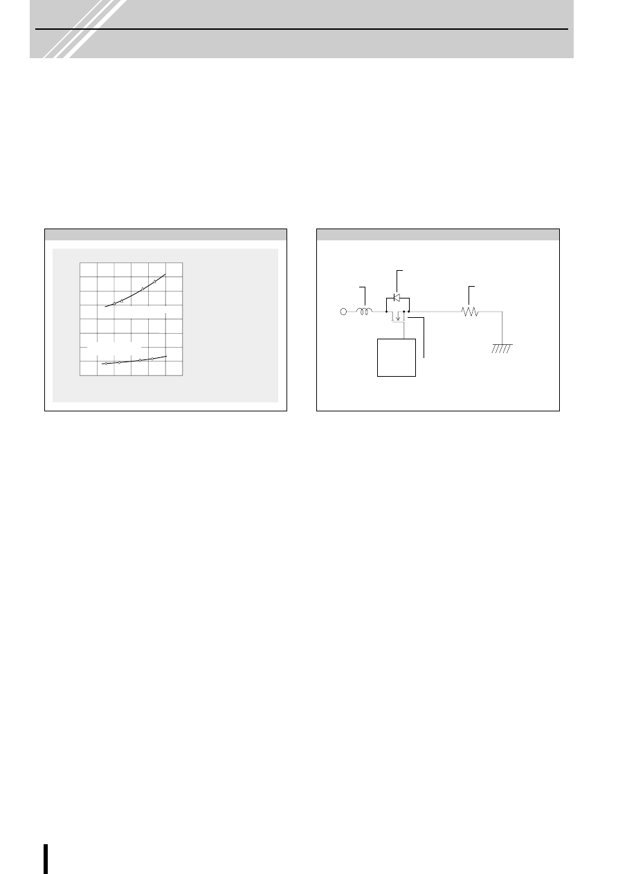
Comparison of power dissipation.
■
Features
●
Employs a constant-current chopper control method.
●
Integrates power MOSFETs and monolithic chip control cir-
cuitry in a single package.
●
One-fifth the size and one-fourth the power dissipation com-
pared with conventional SANKEN ICs
■
Constant Current Chopper Method
In the constant current chopper method, a voltage higher than
the rated voltage of the motor is applied and when the current
rises, the chopper transistor is switched on thereby shortening
the current rise time. After the current rises, the coil current is
held by the PWM chopper to a constant current level deter-
mined by the current sense resistor. This method has the ad-
vantage of improving the motor's high frequency response and
the efficiency response and efficiency of the driver circuitry.
●
Eliminates the need for heatsink thereby decreasing part-in-
sertion workload and increasing flexibility in mounting.
●
Reduces the size of power supplies required.
●
Lineup: 2-phase excitation, 2-phase/1-2 phase excitation,
2W1-2 phase micro-step support ICs
■
Applications
The SLA7000 and SMA7000 series are ideal for the following
applications.
●
Sheet feeders and carriage drivers in printers.
●
Sheet feeders for PPC and facsimile machines.
●
Numeric control equipment.
●
Industrial robots.
■
Handling Precautions
●
Recommended screw torque
0.588 to 0.784 [N
•
m](6.0 to 8.0 [kgf
•
cm])
●
Recommended silicon grease
Shin-Etsu Chemical Co., Ltd.: G746
GE Toshiba Silicone Co., Ltd.: YG-6260
Dow Corning Toray Silicone Co., Ltd.: SC102
Please be careful when selecting silicone grease since the oil
in some grease may penetrate the product, which will result
in an extremely short product life.
Current sense resistor
Motor coil
Transient-suppression diode
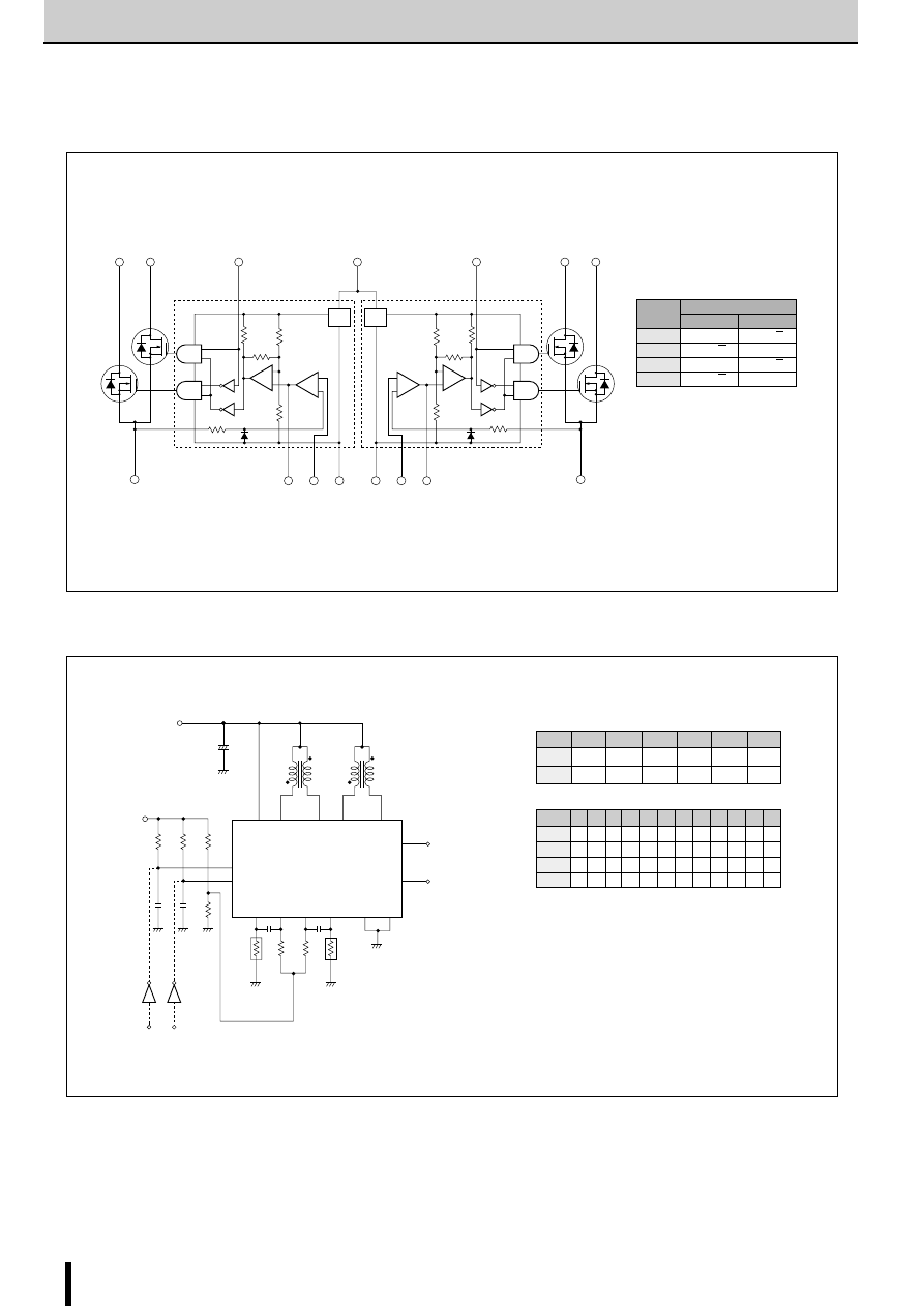
PWM control
and phase
switching
control
V
CC
Used as both chopper
MOSFET and phase
switching MOSFET
Basic constant current chopper circuitry
Notes on SLA7000/SMA7000 Series
Motor Driver ICs
ac/Allegro/Allegro_Motor_Drive_ICs-html.html
5
SLA7022MU/SLA7029M/SMA7022MU/SMA7029M
Parameter
Symbol
Ratings
Units
SLA7022MU
SLA7029M
SMA7022MU
SMA7029M
Motor supply voltage
V
CC
46
V
FET Drain-Source voltage
V
DSS
100
V
Control supply voltage
V
S
46
V
TTL input voltage
V
IN
7
V
Reference voltage
V
REF
2
V
Output current
I
O
1
1.5
1
1.5
A
Power dissipation
P
D1
4.5 (Without Heatsink)
4.0 (Without Heatsink)
W
P
D2
35 (T
C
=25
°
C)
28(T
C
=25
°
C)
W
Channel temperature
T
ch
+150
°
C
Storage temperature
T
stg
−
40 to +150
°
C
■
Absolute Maximum Ratings
2-Phase Stepper Motor Unipolar Driver ICs
SLA7022MU/SLA7029M/SMA7022MU/SMA7029M
2-Phase Excitation
(T
a
=25
°
C)
Ratings
Parameter
Symbol
SLA7022MU
SLA7029M
SMA7022MU
SMA7029M
Units
min
typ
max
min
typ
max
min
typ
max
min
typ
max
Control supply current
I
S
10
15
10
15
10
15
10
15
mA
Condition
V
S
=44V
V
S
=44V
V
S
=44V
V
S
=44V
Control supply voltage
V
S
10
24
44
10
24
44
10
24
44
10
24
44
V
FET Drain-Source
V
DSS
100
100
100
100
V
voltage
Condition
V
S
=44V, I
DSS
=250
µ
A
V
S
=44V, I
DSS
=250
µ
A
V
S
=44V, I
DSS
=250
µ
A
V
S
=44V, I
DSS
=250
µ
A
FET ON voltage
V
DS
0.85
0.6
0.85
0.6
V
Condition
I
D
=1A, V
S
=14V
I
D
=1A, V
S
=14V
I
D
=1A, V
S
=14V
I
D
=1A, V
S
=14V
FET drain leakage current
I
DSS
4
4
4
4
mA
Condition
V
DSS
=100V, V
S
=44V
V
DSS
=100V, V
S
=44V
V
DSS
=100V, V
S
=44V
V
DSS
=100V, V
S
=44V
FET diode forward
V
SD
1.2
1.1
1.2
1.1
V
voltage
Condition
I
D
=1A
I
D
=1A
I
D
=1A
I
D
=1A
I
IH
40
40
40
40
µ
A
TTL input current
Condition
V
IH
=2.4V, V
S
=44V
V
IH
=2.4V, V
S
=44V
V
IH
=2.4V, V
S
=44V
V
IH
=2.4V, V
S
=44V
I
IL
−
0.8
−
0.8
−
0.8
−
0.8
mA
Condition
V
IL
=0.4V, V
S
=44V
V
IL
=0.4V, V
S
=44V
V
IL
=0.4V, V
S
=44V
V
IL
=0.4V, V
S
=44V
V
IH
2
2
2
2
TTL input voltage
Condition
I
D
=1A
I
D
=1A
I
D
=1A
I
D
=1A
V
(Active High)
V
IL
0.8
0.8
0.8
0.8
Condition
V
DSS
=100V
V
DSS
=100V
V
DSS
=100V
V
DSS
=100V
V
IH
2
2
2
2
TTL input voltage
Condition
V
DSS
=100V
V
DSS
=100V
V
DSS
=100V
V
DSS
=100V
V
(Active Low)
V
IL
0.8
0.8
0.8
0.8
Condition
I
D
=1A
I
D
=1A
I
D
=1A
I
D
=1A
T
r
0.5
0.5
0.5
0.5
Condition
V
S
=24V, I
D
=0.8A
V
S
=24V, I
D
=1A
V
S
=24V, I
D
=0.8A
V
S
=24V, I
D
=1A
Switching time
T
stg
0.7
0.7
0.7
0.7
µ
s
Condition
V
S
=24V, I
D
=0.8A
V
S
=24V, I
D
=1A
V
S
=24V, I
D
=0.8A
V
S
=24V, I
D
=1A
T
f
0.1
0.1
0.1
0.1
Condition
V
S
=24V, I
D
=0.8A
V
S
=24V, I
D
=1A
V
S
=24V, I
D
=0.8A
V
S
=24V, I
D
=1A
■
Electrical Characteristics
(T
a
=25
°
C)
DC characteristics
AC characteristics
ac/Allegro/Allegro_Motor_Drive_ICs-html.html
6
SLA7022MU/SLA7029M/SMA7022MU/SMA7029M
SLA7022MU/SLA7029M/SMA7022MU/SMA7029M
2-Phase Stepper Motor Unipolar Driver ICs (2-Phase Excitation)
■
Internal Block Diagram
■
Diagram of Standard External Circuit (Recommended Circuit Constants)
6
Reg
Reg
1
5
8
V
S
14
IN
B
IN
A
7
R
SA
2
3
4
12
13
11
T
DA
REF
A
GND
A
GND
B
REF
B
T
DB
R
SB
9
10
15
+
–
+
–
+
–
+
–
1, 6, 10, 15pin
Description of pins
Excitation input
Active H
OUT A
OUT A
OUT B
OUT B
1pin
6pin
10pin
15pin
Active L
OUT A
OUT A
OUT B
OUT B
8
1
6
10
15
V
S
R
SA
REF
A
REF
B
R
SB
G
A
G
B
7
3 13
9
4
12
C
4
r
6
r
5
r
2
r
1
r
4
r
3
C
1
C
2
T
dA
T
dB
IN
A
IN
B
IN
A
IN
B
5
14
+
V
CC
(46V max)
V
b
(5V)
Rs
Rs
C
3
11
2
Open
collector
t
dA
t
dB
Excitation signal time chart
2-phase excitation
clock
0
1
2
3
0
1
IN
A
H
H
L
L
H
H
IN
B
L
H
H
L
L
H
1-2 phase excitation
clock 0
1
2
3
4
5
6
7
0
1
2 3
IN
A
H H H H
L
L
L
L
H H H H
td
A
L
L
L
H
L
L
L
H L
L
L
H
IN
B
L
L
H H H H
L
L
L
L
H
H
td
B
L H L
L
L
H
L
L
L
H
L
L
●
tdA and tdB are signals before the inverter stage.
r
1
: 510
Ω
r
2
: 100
Ω
(VR)
r
3
: 47k
Ω
r
4
: 47k
Ω
r
5
: 2.4k
Ω
r
6
: 2.4k
Ω
C
1
: 330 to 500pF
C
2
: 330 to 500pF
C
3
: 2200pF
C
4
: 2200pF
R
s
: 1.8
Ω
typ(7022MU)
1
Ω
typ(7029M)
(1 to 2W)
ac/Allegro/Allegro_Motor_Drive_ICs-html.html
7
SLA7022MU/SLA7029M/SMA7022MU/SMA7029M
SLA7022MU/SLA7029M/SMA7022MU/SMA7029M
2-Phase Stepper Motor Unipolar Driver ICs (2-Phase Excitation)
■
External Dimensions SLA7022MU/SLA7029M
(Unit: mm)
31
±
0.2
24.4
±
0.2
16.4
±
0.2
3.2
±
0.15
φ
16
±
0.2
13
±
0.2
9.9
±
0.2
Part No.
Lot No.
3.2
±
0.15
×
3.8
φ
4.8
±
0.2
1.7
±
0.1
2.45
±
0.2
R-End
6.7
±
0.5
9.7
+1 –
0.5
(3)
0.55
+0.2
–0.1
4
±
0.7
1.15
+0.2
–0.1
14
×
P2.03
±
0.7
=28.42
±
1.0
0.65
+0.2
–0.1
31.3
±
0.2
Forming No. No.853
1 2 3 · · · · · · · 15
12 3 · · · · · · · 15
Forming No. No.855
14
×
P2.03
±
0.4
=28.42
±
0.8
0.65
+0.2
–0.1
3
±
0.6
0.55
+0.2 –
0.1
2.2
±
0.4
6.3
±
0.6
7.5
±
0.6
4.6
±
0.6
1.6
±
0.6
Epoxy resin package
1.15
+0.2
–0.1
(Unit: mm)
■
External Dimensions SMA7022MU/SMA7029MA
Forming No. No.1054
31
±
0.2
Part No.
Lot No.
4
±
0.2
2.5
±
0.2
1.45
±
0.15
6.7
±
0.5
(9.7)
(3)
0.55
+0.2
–0.1
4
±
0.7
P2.03
±
0.1
×
14=28.42
0.65
+0.2
–0.1
1 2 3 · · · · · · · 15
12 3 · · · · · · · 15
P2.03
±
0.1
×
14=28.42
1.16
±
0.15
3
±
0.6
0.55
+0.2 –
0.1
1.2
±
0.1
(5.9)
(4.6)
1.6
±
0.6
1.16
+0.2
–0.1
30
°
0.62
±
0.1
(7.5)
Epoxy resin package
8.5ma
x
10.2
±
0.2
31.3
+0.2
Forming No. No.1055
ac/Allegro/Allegro_Motor_Drive_ICs-html.html

8
SLA7022MU/SLA7029M/SMA7022MU/SMA7029M
SLA7022MU/SLA7029M/SMA7022MU/SMA7029M
2-Phase Stepper Motor Unipolar Driver ICs (2-Phase Excitation)
■
Determining the Output Current
Fig. 1 shows the waveform of the output current (motor coil cur-
rent). The method of determining the peak value of the output
current (I
O
) based on this waveform is shown below.
(Parameters for determining the output current I
O
)
V
b
: Reference supply voltage
r
1
,r
2
: Voltage-divider resistors for the reference supply voltage
R
S
: Current sense resistor
(1) Normal rotation mode
I
O
is determined as follows when current flows at the maximum
level during motor rotation. (See Fig.2.)
(2) Power down mode
The circuit in Fig.3 (rx and Tr) is added in order to decrease the
coil current. I
O
is then determined as follows.
Equation (2) can be modified to obtain equation to determine rx.
Fig. 4 and 5 show the graphs of equations (1) and (2) respec-
tively.
(NOTE)
Ringing noise is produced in the current sense resistor R
S
when
the MOSFET is switched ON and OFF by chopping. This noise
is also generated in feedback signals from R
S
which may there-
fore cause the comparator to malfunction. To prevent chopping
malfunctions, r
5
(r
6
) and C
3
(C
4
) are added to act as a noise filter.
R
S
C
3
r
2
r
1
r
6
r
5
V
b
(5
V
)
7,(9)
3,(13)
Fig. 2 Normal mode
0
Phase A
Phase A
I
O
Fig. 1 Waveform of coil current (Phase A excitation ON)
R
S
C
3
r
2
r
1
r
6
r
5
V
b
(5
V
)
7,(9)
3,(13)
r
x
T
r
Power down
signal
Fig. 3 Power down mode
4
3
2
1
0
0
1
2
3
4
Current sense resistor R
S
(
Ω
)
Output current I
O
(A)
I
O
=
r
1
+r
2
R
S
r
1
=510
Ω
r
2
=100
Ω
r
x
=
∞
V
b
=5V
r
2
·
V
b
Fig. 4 Output current I
O
vs. Current sense resistor R
S
Fig. 5 Output current I
OPD
vs. Variable current sense resistor rx
2.0
1.5
1.0
0.5
00
200
400
600
800
Variable current sense resistor r
X
(
Ω
)
Output current I
OPD
(A)
1000
1200
R
S
=0.5
Ω
R
S
=0.8
Ω
R
S
=1
Ω
I
OPD
=
1+ R
S
r
1
=510
Ω
r
2
=100
Ω
V
b
=5V
1
·
V
b
r
1
(r
2+
r
X
)
r
2 ·
r
X
Application Notes
However, when the values of these constants are increased,
the response from R
S
to the comparator becomes slow. Hence
the value of the output current I
O
is somewhat higher than the
calculated value.
r
X
=
1
V
b
R
s
•
I
OPD
1
r
1
−
1
−
1
r
2
................................................................ (1)
I
O
≅
•
r
2
r
1
+r
2
V
b
R
S
......................................................... (2)
I
OPD
≅
•
1
r
1
(r
2
+r
X
)
r
2
•
r
X
V
b
R
S
1+
ac/Allegro/Allegro_Motor_Drive_ICs-html.html
9
SLA7022MU/SLA7029M/SMA7022MU/SMA7029M
SLA7022MU/SLA7029M/SMA7022MU/SMA7029M
2-Phase Stepper Motor Unipolar Driver ICs (2-Phase Excitation)
■
Determining the chopper frequency
Determining T
OFF
The SLA7000M and SMA7000M series are self-excited chop-
pers. The chopping OFF time T
OFF
is fixed by r
3
/C
1
and r
4
/C
2
connected to terminal Td.
T
OFF
can be calculated using the following formula:
The circuit constants and the T
OFF
value shown below are rec-
ommended.
T
OFF
= 12
µ
s at r
3
=47k
Ω
, C
1
=500pF, V
b
=5V
60
50
40
30
20
10
0
0
2
4
6
8
10 12
14
16
15
20
25
30
35
40
Motor coil resistance R
m
(
Ω
)
ON time T
ON
( s)
V
CC
=2
4V
V
CC
=36V
Chopping frequency f (kHz)
T
OFF
=12 s
R
S
=1
Ω
L
m
=1~3ms
R
m
= =
r
3
C
1
r
4
C
2
47k
Ω
500pF
µ
µ
Fig. 6 Chopper frequency vs. Motor coil resistance
■
Chopper frequency vs. Supply voltage
0
f (kHz)
V
CC
(V)
50
40
30
20
10
0
10
20
30
40
50
Motor : 23LM-C202
I
O
= 0.8A at V
CC
=24V
R
S
=1
Ω
■
Chopper frequency vs. Output current
0
f (kHz)
I
O
(A)
50
40
30
20
10
0
0.2
0.4
0.6
0.8
1.0
Motor : 23LM-C202
V
CC
=24V
R
S
=1
Ω
T
OFF
≅−
r
3
•
C
1 n
(1
−
=
−
r
4
•
C
2
n
(1
−
)
r
r
2
V
b
2
V
b
ac/Allegro/Allegro_Motor_Drive_ICs-html.html
10
SLA7022MU/SLA7029M/SMA7022MU/SMA7029M
SLA7022MU/SLA7029M/SMA7022MU/SMA7029M
2-Phase Stepper Motor Unipolar Driver ICs (2-Phase Excitation)
35
30
25
20
15
10
5
0
200
500
1K
Case temperature rise
∆
T
C
–
a
(
°
C)
Motor : PH265-01B
Motor current I
O
=0.8A
T
a
=25
°
C
V
CC
=24V, V
S
=24V
2-phase excitation
Response frequency (pps)
Without heatsink
Natural cooling
T
C
( 4 pin)
30
25
20
15
10
5
0
200
500
1K
Case temperature rise
∆
T
C
–
a
(
°
C)
Motor : PH265-01B
Motor current I
O
=0.8A
T
a
=25
°
C
V
CC
=24V, V
S
=24V
2-phase excitation
Response frequency (pps)
Without heatsink
Natural cooling
T
C
( 4 pin)
Thermal characteristics
SLA7022MU
SLA7029M
SMA7022MU
SMA7029MU
■
Thermal Design
An outline of the method for calculating heat dissipation is shown below.
(1)Obtain the value of P
H
that corresponds to the motor coil
current I
O
from Fig. 7 "Heat dissipation per phase P
H
vs. Out-
put current I
O
."
Output current I
O
(A)
Heat dissipation per phase P
H
(W)
Motor : 23LM-C004
Holding mode
0
0.2
0.4
0.6
0.8
1.0
1.2
1.0
0.8
0.6
0.4
0.2
0
V
CC
=44V
36V
24V
15V
∆
T
j–
a
∆
T
C
–
a
∆
T
j
1
0
2
3
4
∆
T
C
Natural cooling
Without heatsink
150
100
50
0
Total Power (W)
(
°
C)
Fig. 7 Heat dissipation per phase P
H
vs. Output current I
O
Fig. 8 Temperature rise
(2) The power dissipation P
diss
is obtained using the following formula.
2-phase excitation: P
diss
≅
2P
H
+0.015
×
V
S
(W)
1-2 phase excitation: P
diss
≅
P
H
+0.015
×
V
S
(W)
(3) Obtain the temperature rise that corresponds to the calcu-
lated value of P
diss
from Fig. 8 "Temperature rise."
1.2
1
0.8
0.6
0.4
0.2
0
0
0.2
0.4
0.6
0.8
1.0
Heat dissipation per phase P
H
(W)
Output current I
O
(A)
36V
24V
15V
V
CC
=44V
Motor : 23LM-C202
Holding mode
∆
T
j–
a
∆
T
C
–
a
∆
T
j
1
0
2
3
4
5
∆
T
C
Natural cooling
Without heatsink
150
100
50
0
Total Power (W)
(
°
C)
SLA7022MU, ASMA7022MU
SLA7000M series
SLA7029M, SMA7029M
SMA7000M series
3
2
ac/Allegro/Allegro_Motor_Drive_ICs-html.html
11
SLA7022MU/SLA7029M/SMA7022MU/SMA7029M
SLA7022MU/SLA7029M/SMA7022MU/SMA7029M
2-Phase Stepper Motor Unipolar Driver ICs (2-Phase Excitation)
0
Supply current I
CC
(mA)
Supply voltage V
CC
(V)
500
400
300
200
100
0
10
20
30
40
50
Motor : 23LM-C202
1-phase excitation
Holding mode
I
O
: Output current
I
O
=1A
0.4A
0.2A
■
Supply Voltage V
CC
vs. Supply Current I
CC
SLA7022MU, SMA7022MU
0
Supply current I
CC
(mA)
Supply voltage V
CC
(V)
500
400
300
200
100
0
10
20
30
40
50
0.2A
0.5A
I
O
=1A
Motor : 23LM-C004
1-phase excitation
Holding mode
I
O
: Output current
SLA7029M, SMA7029M
100
Pull-out torque (kg-cm)
Response frequency (pps)
2.0
1.5
1.0
0.5
0
5K
1K
500
Motor : 23LM-C202
Output current I
O
=0.8A
Motor supply voltage V
CC
=24V
2-phase excitation
■
Torque Characteristics
SLA7029M, SMA7029M
100
Pull-out torque (kg-cm)
Response frequency (pps)
2.0
1.5
1.0
0.5
0
5K
1K
500
Motor : PX244-02
Output current I
O
=0.6A
Motor supply voltage V
CC
=24V
2-phase excitation
SLA7022MU, SMA7022MU
ac/Allegro/Allegro_Motor_Drive_ICs-html.html
12
SMA7036M
2-Phase Stepper Motor Unipolar Driver IC
SMA7036M
Parameter
Symbol
Ratings
Units
Motor supply voltage
V
CC
46
V
Control supply voltage
V
S
46
V
FET Drain-Source voltage
V
DSS
100
V
TTL input voltage
V
IN
−
0.3 to +7
V
SYNC terminal voltage
V
SYNC
−
0.3 to +7
V
Reference voltage
V
REF
−
0.3 to +7
V
Sense voltage
V
RS
−
5 to +7
V
Output current
I
O
1.5
A
Power dissipation
P
D1
4.0 (T
a
=25
°
C)
W
P
D2
28 (T
c
=25
°
C)
W
Channel temperature
T
ch
150
°
C
Storage temperature
T
stg
−
40 to +150
°
C
Ambient operating temperature
T
a
−
20 to +85
°
C
■
Absolute Maximum Ratings
■
Electrical Characteristics
Parameter
Symbol
Ratings
Units
min
typ
max
Control supply current
I
S
10
15
mA
Condition
V
S
=44V
Control supply voltage
V
S
10
24
44
V
FET Drain-Source
V
DSS
100
V
voltage
Condition
V
S
=44V, I
DSS
=250
µ
A
FET ON voltage
V
DS
0.6
V
Condition
I
D
=1A, V
S
=10V
FET diode forward voltage
V
SD
1.1
V
Condition
I
SD
=1A
FET drain leakage current
I
DSS
250
µ
A
Condition
V
DSS
=100V, V
S
=44V
V
IH
2
Condition
I
D
=1A
V
V
IL
0.8
Condition
V
DSS
=100V
IN terminal
V
IH
2
Condition
V
DSS
=100V
V
V
IL
0.8
Condition
I
D
=1A
I
I
±
1
µ
A
Condition
V
S
=44V, V
I
=0 or 5V
V
SYNC
H
4.0
Condition
Synchronous chopping mode
V
V
SYNC
L
0.8
SYNC terminal
Condition
Asynchronous chopping mode
I
SYNC
H
0.1
Condition
V
S
=44V, V
YS
=5V
mA
I
SYNC
L
−
0.1
Condition
V
S
=44V, V
YS
=0V
V
REF
0
2.0
Condition
Reference voltage input
V
V
REF
4.0
5.5
REF terminal
Condition
Output FET OFF
I
REF
±
1
µ
A
Condition
No synchronous trigger
R
REF
40
Ω
Condition
Resistance between GND and REF terminal at synchronous trigger
T
on
1.5
Condition
V
S
=24V, I
D
=1A
T
r
0.5
Switching time
Condition
V
S
=24V, I
D
=1A
µ
s
T
stg
0.9
Condition
V
S
=24V, I
D
=1A
T
f
0.1
Condition
V
S
=24V, I
D
=1A
Chopping OFF time
T
OFF
12
µ
s
Condition
V
S
=24V
Active H
Active L
Input
current
Input
voltage
Input
current
Input
voltage
Input
current
Internal
resistance
2-Phase Excitation
DC characteristics
AC characteristics
ac/Allegro/Allegro_Motor_Drive_ICs-html.html
13
SMA7036M
SMA7036M
2-Phase Stepper Motor Unipolar Driver IC (2-Phase Excitation)
■
Internal Block Diagram
■
Diagram of Standard External Circuit (Recommended Circuit Constants)
Excitation signal time chart
2-phase excitation
clock
0
1
2
3
0
1
IN
A
H
H
L
L
H
H
IN
B
L
H
H
L
L
H
r
1
: 8k
Ω
r
2
: 2k
Ω
(VR)
R
S
(1 to 2W) : 1
Ω
typ
PchMOS
: HN1J02FU (Toshiba)
Inv
: 7404
5
8
14
10
15
1, 6, 10, 15pin
Description of pins
6
1
7
2
4
3
13
12
11
9
Chopping
blanking timer
(5 s typ)
µ
Chopping
blanking timer
(5 s typ)
Chopping
OFF timer
(12 s typ)
µ
Chopping
OFF timer
(12 s typ)
Synchronous
chopping
circuit
Synchronous
chopping
circuit
MOSFET
gate drive
circuit
MOSFET
gate drive
circuit
IN A
IN B
Vs
Rs A
SYNC A
SYNC B
GND A
REF A
REF B
GND B
Oscillator
Oscillator
Reg.
Reg.
Rs B
+
−
+
−
Excitation input
Active H
OUT A
OUT A
OUT B
OUT B
1pin
6pin
10pin
15pin
Active L
OUT A
OUT A
OUT B
OUT B
µ
µ
Disable (High Active)
Vb (5V)
Vcc (46V max)
PchMOS
2
11
5
14
Inv
r2
7
8
+
1
6
10
15
IN
B
IN
A
Rs
Rs
3
13
12
9
4
r1
SMA7036M
Sync
B
IN
B
IN
A
V
S
Rs
A
G
A
G
B
Rs
B
Ref
A
Ref
B
Sync
A
ac/Allegro/Allegro_Motor_Drive_ICs-html.html
14
SMA7036M
SMA7036M
2-Phase Stepper Motor Unipolar Driver IC (2-Phase Excitation)
(Unit: mm)
■
External Dimensions
Forming No. No.1054
31
±
0.2
Part No.
Lot No.
4
±
0.2
2.5
±
0.2
1.45
±
0.15
6.7
±
0.5
(9.7)
(3)
0.55
+0.2
–0.1
4
±
0.7
P2.03
±
0.1
×
14=28.42
0.65
+0.2
–0.1
1 2 3 · · · · · · · 15
12 3 · · · · · · · 15
P2.03
±
0.1
×
14=28.42
1.16
±
0.15
3
±
0.6
0.55
+0.2 –0.1
1.2
±
0.1
(5.9)
(4.6)
1.6
±
0.6
1.16
+0.2
–0.1
30
°
0.62
±
0.1
(7.5)
Epoxy resin package
8.5ma
x
10.2
±
0.2
31.3
+0.2
Forming No. No.1055
ac/Allegro/Allegro_Motor_Drive_ICs-html.html
15
SMA7036M
SMA7036M
2-Phase Stepper Motor Unipolar Driver IC (2-Phase Excitation)
■
Outline
SMA7036M is a stepper motor driver IC developed to reduce
the number of external parts required by the conventional
SMA7029M. This IC successfully eliminates the need for some
external parts without sacrificing the features of SMA7029M.
The basic function pins are compatible with those of SMA7029M.
■
Notes on Replacing SMA7029M
SMA7036M is pin-compatible with SMA7029M. When using
the IC on an existing board, the following preparations are nec-
essary:
(1) Remove the resistors and capacitors attached for setting
the chopping OFF time. (r
3
, r
4
, C
1
, and C
2
in the catalog)
(2) Remove the resistors and capacitors attached for preventing
noise in the detection voltage V
RS
from causing malfunction-
ing and short the sections from which the resistors were re-
moved using jumper wires. (r
5
, r
6
, C
3
, and C
4
in the catalog)
(3) Normally, keep pins 2 and 11 grounded because their func-
tions have changed to synchronous and asynchronous
switching (SYNC terminals). For details, see "Circuit for Pre-
venting Abnormal Noise When the Motor Is Not Running (Syn-
chronous circuit)." (Low: asynchronous, High: synchronous)
■
Circuit for Preventing Abnormal Noise When the
Motor Is Not Running (Synchronous Circuit)
A motor may generate abnormal noise when it is not running.
This phenomenon is attributable to asynchronous chopping be-
tween phases A and B. To prevent the phenomenon, SMA7036M
contains a synchronous chopping circuit. Do not leave the SYNC
terminals open because they are for CMOS input.
■
Synchronous circuit operating waveform
SYNC_A
SYNC voltage : Low
SYNC voltage : High
→
Chopping asynchronous
→
Chopping synchronous
TTL, etc.
SYNC_B
SMA7036M
ONE SHOT
(tw=2 S)
Sync/async
switching signal
To comparator
(high impedance)
REF_A
R1
R2
3
5V
REF_B
V
REF
V
REF
waveform
V
REF
0
14
SMA7036M
FET A/A
gate drive signal
40
Ω
(typ.)
40
Ω
(typ.)
FET B/B
gate drive signal
ONE SHOT
(tw=2 S)
µ
µ
V
REF
V
RS
Phase A
0
V
REF
V
RS
Synchronous circuit ON
Synchronous circuit OFF
Phase B
0
Application Notes
Connect TTL or similar to the SYNC terminals and switch the
SYNC terminal level high or low.
When the motor is not running, set the TTL signal high (SYNC
terminal voltage: 4 V or more) to make chopping synchronous.
When the motor is running, set the TTL signal low (SYNC terminal
voltage: 0.8 V or less) to make chopping asynchronous. If chop-
ping is set to synchronous when the motor is running, the motor
torque deteriorates before the coil current reaches the set value.
If no abnormal noise occurs when the motor is not running,
ground the SYNC terminals (TTL not necessary).
The built-in synchronous chopping circuit superimposes a trigger
signal on the REF terminal for synchronization between the two
phases. The figure below shows the internal circuit of the REF
terminal. Since the
∆
V
REF
varies depending on the values of R1
and R2, determine these values for when the motor is not run-
ning within the range where the two phases are synchronized.
ac/Allegro/Allegro_Motor_Drive_ICs-html.html
16
SMA7036M
SMA7036M
2-Phase Stepper Motor Unipolar Driver IC (2-Phase Excitation)
0
Phase A
Phase A
I
O
R
S
r
2
r
1
V
b
(5
V
)
7,(9)
3,(13)
R
S
r
2
r
1
V
b
(5
V
)
7,(9)
3,(13)
r
x
T
r
Power down
signal
■
Determining the Output Current
Fig. 1 shows the waveform of the output current (motor coil cur-
rent). The method of determining the peak value of the output
current (I
O
) based on this waveform is shown below.
(Parameters for determining the output current I
O
)
V
b
: Reference supply voltage
r
1
,r
2
: Voltage-divider resistors for the reference supply voltage
R
S
: Current sense resistor
(1) Normal rotation mode
I
O
is determined as follows when current flows at the maximum
level during motor rotation. (See Fig.2.)
(2) Power down mode
The circuit in Fig.3 (r
x
and T
r
) is added in order to decrease the
coil current. I
O
is then determined as follows.
Equation (2) can be modified to obtain equation to determine rx.
Fig. 4 and 5 show the graphs of equations (1) and (2) respec-
tively.
Fig. 2 Normal mode
Fig. 1 Waveform of coil current (Phase A excitation ON)
Fig. 3 Power down mode
4
3
2
1
0
0
1
2
3
4
Current sense resistor R
S
(
Ω
)
Output current I
O
(A)
I
O
=
r
1
+r
2
R
S
r
1
=510
Ω
r
2
=100
Ω
r
x
=
∞
V
b
=5V
r
2
·
V
b
Fig. 4 Output current I
O
vs. Current sense resistor R
S
Fig. 5 Output current I
OPD
vs. Variable current sense resistor rx
2.0
1.5
1.0
0.5
00
200
400
600
800
Variable current sense resistor r
X
(
Ω
)
Output current I
OPD
(A)
1000
1200
R
S
=0.5
Ω
R
S
=0.8
Ω
R
S
=1
Ω
I
OPD
=
1+ R
S
r
1
=510
Ω
r
2
=100
Ω
V
b
=5V
1
·
V
b
r
1
(r
2+
r
X
)
r
2 ·
r
X
r
X
=
1
V
b
R
s
•
I
OPD
1
r
1
−
1
−
1
r
2
................................................................ (1)
I
O
≅
•
r
2
r
1
+r
2
V
b
R
S
......................................................... (2)
I
OPD
≅
•
1
r
1
(r
2
+r
X
)
r
2
•
r
X
V
b
R
S
1+
ac/Allegro/Allegro_Motor_Drive_ICs-html.html
17
SMA7036M
SMA7036M
2-Phase Stepper Motor Unipolar Driver IC (2-Phase Excitation)
Output current I
O
(A)
Heat dissipation per phase P
H
(W)
Motor : 23LM-C004
Holding mode
0
0.2
0.4
0.6
0.8
1.0
1.2
1.0
0.8
0.6
0.4
0.2
0
V
CC
=44V
36V
24V
15V
Fig. 6 Heat dissipation per phase P
H
vs. Output current I
O
∆
T
j–
a
∆
T
C
–
a
∆
T
j
1
0
2
3
4
∆
T
C
Natural cooling
Without heatsink
150
100
50
0
Total Power (W)
(
°
C)
Fig. 7 Temperature rise
Thermal characteristics
30
25
20
15
10
5
0
200
500
1K
Case temperature rise
∆
T
C
–
a
(
°
C)
Motor : PH265-01B
Motor current I
O
=0.8A
T
a
=25
°
C
V
CC
=24V, V
S
=24V
2-phase excitation
Response frequency (pps)
Without heatsink
Natural cooling
T
C
( 4 pin)
■
Thermal Design
An outline of the method for calculating heat dissipation is
shown below.
(1) Obtain the value of P
H
that corresponds to the motor coil
current I
O
from Fig. 6 "Heat dissipation per phase P
H
vs. Out-
put current I
O
."
(2) The power dissipation P
diss
is obtained using the following
formula.
2-phase excitation: P
diss
≅
2P
H
+0.015
×
V
S
(W)
1-2 phase excitation: P
diss
≅
P
H
+0.015
×
V
S
(W)
(3) Obtain the temperature rise that corresponds to the calcu-
lated value of P
diss
from Fig. 7 "Temperature rise."
3
2
ac/Allegro/Allegro_Motor_Drive_ICs-html.html
18
SMA7036M
SMA7036M
2-Phase Stepper Motor Unipolar Driver IC (2-Phase Excitation)
■
Handling Precautions
The input terminals of this product use C-MOS circuits. Observe the following precautions.
●
Carefully control the humidity of the room to prevent the buildup of static electricity. Since static electricity is particularly a problem
during the winter, be sure to take sufficient precautions.
●
Take care to make sure that static electricity is not applied to the IC during wiring and assembly. Take precautions such as shorting
the terminals of the printed wiring board to ensure that they are at the same electrical potential.
■
Chopper frequency vs. Supply voltage
■
Chopper frequency vs. Output current
0
f (kHz)
V
CC
(V)
50
40
30
20
10
0
10
20
30
40
50
Motor : 23LM-C202
I
O
= 0.8A at V
CC
=24V
R
S
=1
Ω
0
f (kHz)
I
O
(A)
50
40
30
20
10
0
0.2
0.4
0.6
0.8
1.0
Motor : 23LM-C202
V
CC
=24V
R
S
=1
Ω
■
Supply Voltage V
CC
vs. Supply Current I
CC
0
Supply current I
CC
(mA)
Supply voltage V
CC
(V)
500
400
300
200
100
0
10
20
30
40
50
0.2A
0.5A
I
O
=1A
Motor : 23LM-C004
1-phase excitation
Holding mode
I
O
: Output current
■
Torque Characteristics
100
Pull-out torque (kg-cm)
Response frequency (pps)
2.0
1.5
1.0
0.5
0
5K
1K
500
Motor : 23LM-C202
Output current I
O
=0.8A
Motor supply voltage V
CC
=24V
2-phase excitation
ac/Allegro/Allegro_Motor_Drive_ICs-html.html

19
SMA7036M
ac/Allegro/Allegro_Motor_Drive_ICs-html.html
20
SLA7027MU/SLA7024M/SLA7026M
Parameter
Symbol
Ratings
Units
SLA7027MU
SLA7024M
SLA7026M
Motor supply voltage
V
CC
46
V
FET Drain-Source voltage
V
DSS
100
V
Control supply voltage
V
S
46
V
TTL input voltage
V
IN
7
V
Reference voltage
V
REF
2
V
Output current
I
O
1
1.5
3
A
Power dissipation
P
D1
4.5 (Without Heatsink)
W
P
D2
35 (T
C
=25
°
C)
W
Channel temperature
T
ch
+150
°
C
Storage temperature
T
stg
−
40 to +150
°
C
■
Electrical Characteristics
■
Absolute Maximum Ratings
2-Phase Stepper Motor Unipolar Driver ICs
SLA7027MU/SLA7024M/SLA7026M
2-Phase/1-2 Phase Excitation
(Ta=25
°
C)
Ratings
Parameter
Symbol
SLA7027MU
SLA7024M
SLA7026M
Units
min
typ
max
min
typ
max
min
typ
max
Control supply current
I
S
10
15
10
15
10
15
mA
Condition
V
S
=44V
V
S
=44V
V
S
=44V
Control supply voltage
V
S
10
24
44
10
24
44
10
24
44
V
FET Drain-Source voltage
V
DSS
100
100
100
V
Condition
V
S
=44V, I
DSS
=250
µ
A
V
S
=44V, I
DSS
=250
µ
A
V
S
=44V, I
DSS
=250
µ
A
FET ON voltage
V
DS
0.85
0.6
0.85
V
Condition
I
D
=1A, AV
S
=14V
I
D
=1A, V
S
=14V
I
D
=3A, V
S
=14V
FET drain leakage current
I
DSS
4
4
4
mA
Condition
V
DSS
=100V, V
S
=44V
V
DSS
=100V, V
S
=44V
V
DSS
=100V, V
S
=44V
FET diode forward voltage
V
SD
1.2
1.1
2.3
V
Condition
I
D
=1A
I
D
=1A
I
D
=3A
I
IH
40
40
40
µ
A
TTL input current
Condition
V
IH
=2.4V, V
S
=44V
V
IH
=2.4V, V
S
=44V
V
IH
=2.4V, V
S
=44V
I
IL
−
0.8
−
0.8
−
0.8
mA
Condition
V
IL
=0.4V, V
S
=44V
V
IL
=0.4V, V
S
=44V
V
IL
=0.4V, V
S
=44V
V
IH
2
2
2
TTL input voltage
Condition
I
D
=1A
I
D
=1A
I
D
=3A
V
(Active High)
V
IL
0.8
0.8
0.8
Condition
V
DSS
=100V
V
DSS
=100V
V
DSS
=100V
V
IH
2
2
2
TTL input voltage
Condition
V
DSS
=100V
V
DSS
=100V
V
DSS
=100V
V
(Active Low)
V
IL
0.8
0.8
0.8
Condition
I
D
=1A
I
D
=1A
I
D
=3A
T
r
0.5
0.5
0.5
Condition
V
S
=24V, I
D
=0.8A
V
S
=24V, I
D
=1A
V
S
=24V, I
D
=1A
Switching time
T
stg
0.7
0.7
0.7
µ
s
Condition
V
S
=24V, I
D
=0.8A
V
S
=24V, I
D
=1A
V
S
=24V, I
D
=1A
T
f
0.1
0.1
0.1
Condition
V
S
=24V, I
D
=0.8A
V
S
=24V, I
D
=1A
V
S
=24V, I
D
=1A
DC characteristics
AC characteristics
ac/Allegro/Allegro_Motor_Drive_ICs-html.html
21
SLA7027MU/SLA7024M/SLA7026M
SLA7027MU/SLA7024M/SLA7026M
2-Phase Stepper Motor Unipolar Driver ICs (2-Phase/1-2 Phase Excitation)
■
Internal Block Diagram
■
Diagram of Standard External Circuit(Recommended Circuit Constants)
1, 8, 11, 18pin
Description of pins
Excitation input
Active H
Active L
Pin 1
OUT
A
OUT
A
Pin 8
OUT
A
OUT
A
Pin 11
OUT
B
OUT
B
Pin 18
OUT
B
OUT
B
Reg
IN A
V
SA
R
SA
2
3
4
G
A
T
DA
REF
A
9
Reg
IN A
8
1
6
5
7
12
17
16
18
11
IN B
IN B
V
SB
G
B
T
DB
REF
B
R
SB
14
13
15
10
+
–
+
–
+
–
+
–
Active High
7 12
8
1
18
11
V
SA
V
SB
OUT
A
OUT
B
OUT
B
OUT
A
R
SA
REF
A
REF
B
R
SB
G
A
G
B
9
3 14
10
4
15
C
4
r
6
r
5
r
2
r
1
r
4
r
3
C
1
C
2
13
T
dA
T
dB
IN
A
IN
A
IN
B
IN
B
IN
A
IN
A
IN
B
IN
B
6
5
17
16
Active
High
+
V
CC
(46V max)
V
b
(5V)
Rs
Rs
C
3
SLA7024M
7026M
7027MU
2
Active Low
7 12
8
1
18
11
V
SA
V
SB
OUT
A
OUT
B
OUT
B
OUT
A
R
SA
REF
A
REF
B
R
SB
G
A
G
B
9
3 14
10
4
15
C
4
r
6
r
5
r
2
r
1
r
4
r
3
C
1
C
2
13
T
dA
T
dB
IN
A
IN
A
IN
B
IN
B
IN
A
IN
A
IN
B
IN
B
6
5
17
16
Active
Low
+
V
CC
(46V max)
V
b
(5V)
Rs
Rs
C
3
SLA7024M
7026M
7027MU
2
r
1
: 510
Ω
r
2
: 100
Ω
(VR)
r
3
: 47k
Ω
r
4
: 47k
Ω
r
5
: 2.4k
Ω
r
6
: 2.4k
Ω
C
1
: 470pF
C
2
: 470pF
C
3
: 2200pF
C
4
: 2200pF
R
s
: 1
Ω
typ(7024M)
0.68
Ω
typ(7026M)
1.8
Ω
typ(7027MU)
1-2 phase excitation
clock
0
1
2
3
4
5
6
7
0
1
2
3
IN
A
L
L
H H H H H
L
L
L
H H
IN
A
H H H
L
L
L
H H H H H L
IN
B
H
L
L
L
H H H H H
L
L
L
IN
B
H H H H H L
L
L
H H H H
r
1
: 510
Ω
r
2
: 100
Ω
(VR)
r
3
: 47k
Ω
r
4
: 47k
Ω
r
5
: 2.4k
Ω
r
6
: 2.4k
Ω
C
1
: 470pF
C
2
: 470pF
C
3
: 2200pF
C
4
: 2200pF
R
s
: 1
Ω
typ(7024M)
0.68
Ω
typ(7026M)
1.8
Ω
typ(7027MU)
(1 to 2W)
1-2 phase excitation
clock
0
1
2
3
4
5
6
7
0
1
2
3
IN
A
H H L
L
L
L
L
H H H
L
L
IN
A
L
L
L
H H H
L
L
L
L
L
H
IN
B
L
H H H
L
L
L
L
L
H H H
IN
B
L
L
L
L
L
H H H
L
L
L
L
Excitation signal time chart
2-phase excitation
clock
0
1
2
3
0
1
IN
A
H
L
L
H
H
L
IN
A
L
H
H
L
L
H
IN
B
H
H
L
L
H
H
IN
B
L
L
H
H
L
L
Excitation signal time chart
2-phase excitation
clock
0
1
2
3
0
1
IN
A
L
H
H
L
L
H
IN
A
H
L
L
H
H
L
IN
B
L
L
H
H
L
L
IN
B
H
H
L
L
H
H
(1 to 2W)
ac/Allegro/Allegro_Motor_Drive_ICs-html.html
22
SLA7027MU/SLA7024M/SLA7026M
2-Phase Stepper Motor Unipolar Driver ICs (2-Phase/1-2 Phase Excitation)
SLA7027MU/SLA7024M/SLA7026M
■
External Dimensions
(Unit: mm)
31
±
0.2
24.4
±
0.2
16.4
±
0.2
3.2
±
0.15
φ
16
±
0.2
13
±
0.2
9.9
±
0.2
Part No.
Lot No.
3.2
±
0.15
×
3.8
φ
4.8
±
0.2
1.7
±
0.1
2.45
±
0.2
R-End
6.7
±
0.5
9.7
+1 –
0.5
(3)
0.55
+0.2
–0.1
4
±
0.7
1
+0.2
–0.1
17
×
P1.68
±
0.4
=28.56
±
1
0.65
+0.2
–0.1
31.3
±
0.2
Forming No. No.871
Forming No. No.872
1 2 3 · · · · · · · 18
123 · · · · · · · 18
17
×
P1.68
±
0.4
=28.56
±
1
0.65
+0.2
–0.1
1
+0.2
–0.1
3
±
0.6
0.55
+0.2 –
0.1
2.2
±
0.6
6
±
0.6
7.5
±
0.6
4.6
±
0.6
1.6
±
0.6
3.
4.
5.
ac/Allegro/Allegro_Motor_Drive_ICs-html.html
23
SLA7027MU/SLA7024M/SLA7026M
SLA7027MU/SLA7024M/SLA7026M
2-Phase Stepper Motor Unipolar Driver ICs (2-Phase/1-2 Phase Excitation)
R
S
C
3
r
2
r
1
r
6
r
5
V
b
(5
V
)
9,(10)
3,(14)
C
3
r
2
r
1
r
6
r
5
V
b
(5
V
)
9,(10)
3,(14)
r
X
T
r
Power down
signal
■
Determining the Output Current
Fig. 1 shows the waveform of the output current (motor coil cur-
rent). The method of determining the peak value of the output
current (I
O
) based on this waveform is shown below.
(Parameters for determining the output current I
O
)
V
b
: Reference supply voltage
r
1
,r
2
: Voltage-divider resistors for the reference supply voltage
R
S
: Current sense resistor
(1) Normal rotation mode
I
O
is determined as follows when current flows at the maximum
level during motor rotation. (See Fig.2.)
(2) Power down mode
The circuit in Fig.3 (rx and Tr) is added in order to decrease the
coil current. I
O
is then determined as follows.
Equation (2) can be modified to obtain equation to determine rx.
Fig. 4 and 5 show the graphs of equations (1) and (2) respec-
tively.
(NOTE)
Ringing noise is produced in the current sense resistor R
S
when
the MOSFET is switched ON and OFF by chopping. This noise
is also generated in feedback signals from R
S
which may there-
fore cause the comparator to malfunction. To prevent chopping
malfunctions, r
5
(r
6
) and C
3
(C
4
) are added to act as a noise filter.
Fig. 2 Normal mode
0
Phase A
Phase A
I
O
Fig. 1 Waveform of coil current (Phase A excitation ON)
Fig. 3 Power down mode
4
3
2
1
0
0
1
2
3
4
Current sense resistor R
S
(
Ω
)
Output current I
O
(A)
I
O
=
r
1
+r
2
R
S
r
1
=510
Ω
r
2
=100
Ω
r
x
=
∞
V
b
=5V
r
2
·
V
b
Fig. 4 Output current I
O
vs. Current sense resistor R
S
Fig. 5 Output current I
OPD
vs. Variable current sense resistor rx
2.0
1.5
1.0
0.5
00
200
400
600
800
Variable current sense resistor r
X
(
Ω
)
Output current I
OPD
(A)
1000
1200
R
S
=0.5
Ω
R
S
=0.8
Ω
R
S
=1
Ω
I
OPD
=
1+ R
S
r
1
=510
Ω
r
2
=100
Ω
V
b
=5V
1
·
V
b
r
1
(r
2+
r
X
)
r
2 ·
r
X
Application Notes
r
X
=
1
V
b
R
s
•
I
OPD
1
r
1
−
1
−
1
r
2
However, when the values of these constants are increased,
the response from R
S
to the comparator becomes slow. Hence
the value of the output current I
O
is somewhat higher than the
calculated value.
................................................................ (1)
I
O
≅
•
r
2
r
1
+r
2
V
b
R
S
......................................................... (2)
I
OPD
≅
•
1
r
1
(r
2
+r
X
)
r
2
•
r
X
V
b
R
S
1+
ac/Allegro/Allegro_Motor_Drive_ICs-html.html

24
SLA7027MU/SLA7024M/SLA7026M
2-Phase Stepper Motor Unipolar Driver ICs (2-Phase/1-2 Phase Excitation)
SLA7027MU/SLA7024M/SLA7026M
Fig. 6 Chopper frequency vs. Motor coil resistance
60
50
40
30
20
10
0
0
2
4
6
8
10 12
14
16
15
20
25
30
35
40
Motor coil resistance R
m
(
Ω
)
ON time T
ON
( s)
V
CC
=24V
V
CC
=36V
Chopping frequency f (kHz)
T
OFF
=12 s
R
S
=1
Ω
L
m
=1~3ms
R
m
= =
r
3
C
1
r
4
C
2
47k
Ω
500pF
µ
µ
■
Determining the chopper frequency
Determining T
OFF
The SLA7000M series are self-excited choppers. The chopping
OFF time T
OFF
is fixed by r
3
/C
1
and r
4
/C
2
connected to terminal
Td.
T
OFF
can be calculated using the following formula:
The circuit constants and the T
OFF
value shown below are rec-
ommended.
T
OFF
= 12
µ
s at r
3
=47k
Ω
, C
1
=500pF, V
b
=5V
■
Chopper frequency vs. Supply voltage
0
f (kHz)
V
CC
(V)
50
40
30
20
10
0
10
20
30
40
50
Motor : 23LM-C202
I
O
= 0.8A at V
CC
=24V
R
S
=1
Ω
■
Chopper frequency vs. Output current
0
f (kHz)
I
O
(A)
50
40
30
20
10
0
0.2
0.4
0.6
0.8
1.0
Motor : 23LM-C202
V
CC
=24V
R
S
=1
Ω
T
OFF
≅−
r
3
•
C
1 n
(1
−
=
−
r
4
•
C
2
n
(1
−
)
r
r
2
V
b
2
V
b
ac/Allegro/Allegro_Motor_Drive_ICs-html.html
25
SLA7027MU/SLA7024M/SLA7026M
SLA7027MU/SLA7024M/SLA7026M
2-Phase Stepper Motor Unipolar Driver ICs (2-Phase/1-2 Phase Excitation)
Thermal characteristics
Fig. 7 Heat dissipation per phase P
H
vs. Output current I
O
SLA7027MU
SLA7024M
1.2
1
0.8
0.6
0.4
0.2
0
0
0.2
0.4
0.6
0.8
1.0
Heat dissipation per phase P
H
(W)
Output current I
O
(A)
36V
24V
15V
V
CC
=44V
Motor : 23LM-C202
Holding mode
Output current I
O
(A)
Heat dissipation per phase P
H
(W)
Motor : 23LM-C004
Holding mode
0
0.2
0.4
0.6
0.8
1.0
1.2
1.0
0.8
0.6
0.4
0.2
0
V
CC
=44V
36V
24V
15V
Heat dissipation per phase P
H
(W)
Motor : 23PM-C503
Holding mode
36V
15V
24V
V
C
C
=44V
4.0
3.0
2.0
1.0
0
0
1.0
2.0
3.0
Output current I
O
(A)
SLA7026M
SLA7027MU
35
30
25
20
15
10
5
0
200
500
1K
Case temperature rise
∆
T
C
–
a
(
°
C)
Motor : PH265-01B
Motor current I
O
=0.8A
T
a
=25
°
C
V
CC
=24V, V
S
=24V
2-phase excitation
Response frequency (pps)
Without heatsink
Natural cooling
T
C
( 4 pin)
30
25
20
15
10
5
0
200
500
1K
Case temperature rise
∆
T
C
–
a
(
°
C)
Motor : PH265-01B
Motor current I
O
=0.8A
T
a
=25
°
C
V
CC
=24V, V
S
=24V
2-phase excitation
Response frequency (pps)
Without heatsink
Natural cooling
T
C
( 4 pin)
50
40
30
20
10
0
100
500
1K
5K
Case temper
ature r
ise
∆
T
C
–
a
(
°
C)
Response frequency (pps)
Without heatsink
Natural cooling
Motor : 23PM-C705
Motor current I
O
=1.5A
T
a
=25
°
C
V
CC
=24V, V
S
=24V
2-phase excitation
T
C
( 4 pin)
SLA7024M
SLA7026M
Fig. 8 Temperature rise
∆
T
j–
a
∆
T
C
–
a
∆
T
j
1
0
2
3
4
5
∆
T
C
Natural cooling
Without heatsink
150
100
50
0
Total Power (W)
(
°
C)
■
Thermal Design
An outline of the method for calculating heat dissipation is shown be-
low.
(1) Obtain the value of P
H
that corresponds to the motor coil current
I
O
from Fig. 7 "Heat dissipation per phase P
H
vs. Output current I
O
."
(2) The power dissipation Pdiss is obtained using the following formula.
2-phase excitation: P
diss
≅
2P
H
+0.015
×
V
S
(W)
1-2 phase excitation: P
diss
≅
P
H
+0.015
×
V
S
(W)
(3) Obtain the temperature rise that corresponds to the calcu-
lated value of Pdiss from Fig. 8 "Temperature rise."
3
2
ac/Allegro/Allegro_Motor_Drive_ICs-html.html
26
SLA7027MU/SLA7024M/SLA7026M
2-Phase Stepper Motor Unipolar Driver ICs (2-Phase/1-2 Phase Excitation)
SLA7027MU/SLA7024M/SLA7026M
■
Note
The excitation input signals of the SLA7027MU, SLA7024M and SLA7026M can be used as either Active High or Active Low. Note,
however, that the corresponding output (OUT) changes depending on the input (IN).
Active Low
Input
Corresponding output
IN
A
(pin6)
OUT
A
(pin8)
IN
A
(pin5)
OUT
A
(pin1)
IN
B
(pin17)
OUT
B
(pin18)
IN
B
(pin16)
OUT
B
(pin11)
Active High
Input
Corresponding output
IN
A
(pin6)
OUT
A
(pin1)
IN
A
(pin5)
OUT
A
(pin8)
IN
B
(pin17)
OUT
B
(pin11)
IN
B
(pin16)
OUT
B
(pin18)
■
Supply Voltage V
CC
vs. Supply Current I
CC
0
Supply current I
CC
(mA)
Supply voltage V
CC
(V)
500
400
300
200
100
0
10
20
30
40
50
Motor : 23LM-C202
1-phase excitation
Holding mode
I
O
: Output current
I
O
=1A
0.4A
0.2A
0
Supply current I
CC
(mA)
Supply voltage V
CC
(V)
500
400
300
200
100
0
10
20
30
40
50
0.2A
0.5A
I
O
=1A
Motor : 23LM-C004
1-phase excitation
Holding mode
I
O
: Output current
0
Supply current I
CC
(A)
Supply voltage V
CC
(V)
1.5
1.0
0.5
0
10
20
30
40
50
Motor : 23PM-C503
1-phase excitation
Holding mode
I
O
: Output current
I
O
=1A
I
O
=2A
I
O
=3A
SLA7027MU
SLA7024M
SLA7026M
ac/Allegro/Allegro_Motor_Drive_ICs-html.html

27
SLA7027MU/SLA7024M/SLA7026M
ac/Allegro/Allegro_Motor_Drive_ICs-html.html
28
SLA7032M/SLA7033M
Ratings
Parameter
Symbol
SLA7032M
SLA7033M
Units
min
typ
max
min
typ
max
Control supply current
I
S
10
15
10
15
mA
Condition
V
S
=44V
V
S
=44V
Control supply voltage
V
S
10
24
44
10
24
44
V
FET Drain-Source
V
DSS
100
100
V
voltage
Condition
V
S
=44V, I
DSS
=250
µ
A
V
S
=44V, I
DSS
=250
µ
A
FET ON voltage
V
DS
0.6
0.85
V
Condition
I
D
=1A, V
S
=14V
I
D
=3A, V
S
=14V
FET diode forward voltage
V
SD
1.1
2.3
V
Condition
I
SD
=1A
I
SD
=3A
FET drain leakage current
I
DSS
250
250
µ
A
Condition
V
DSS
=100V, V
S
=44V
V
DSS
=100V, V
S
=44V
V
IH
2.0
2.0
Condition
I
D
=1A
I
D
=3A
V
V
IL
0.8
0.8
Condition
V
DSS
=100V
V
DSS
=100V
IN terminal
V
IH
2.0
2.0
Condition
V
DSS
=100V
V
DSS
=100V
V
V
IL
0.8
0.8
Condition
I
D
=1A
I
D
=3A
I
I
±
1
±
1
µ
A
Condition
V
S
=44V, V
I
=0 or 5V
V
S
=44V, V
I
=0 or 5V
V
SYNC
4.0
4.0
Condition
Synchronous chopping mode
Synchronous chopping mode
V
V
SYNC
0.8
0.8
SYNC terminal
Condition
Asynchronous chopping mode
Asynchronous chopping mode
I
SYNC
0.1
0.1
Condition
V
S
=44V, V
YS
=5V
V
S
=44V, V
YS
=5V
mA
I
SYNC
−
0.1
−
0.1
Condition
V
S
=44V, V
YS
=0V
V
S
=44V, V
YS
=0V
V
REF
0
2.0
0
2.0
Condition
Reference voltage input
Reference voltage input
V
V
REF
4.0
5.5
4.0
5.5
REF terminal
Condition
Output FET OFF
Output FET OFF
I
REF
±
1
±
1
µ
A
Condition
No synchronous trigger
No synchronous trigger
R
REF
40
40
Ω
Condition Resistance between GND and REF terminal at synchronous trigger
Resistance between GND and REF terminal at synchronous trigger
T
r
0.5
0.5
Condition
V
S
=24V, I
D
=1A
V
S
=24V, I
D
=1A
Switching time
T
stg
0.7
0.7
µ
s
Condition
V
S
=24V, I
D
=1A
V
S
=24V, I
D
=1A
T
f
0.1
0.1
Condition
V
S
=24V, I
D
=1A
V
S
=24V, I
D
=1A
Chopping OFF time
T
OFF
12
12
µ
s
Condition
V
S
=24V
V
S
=24V
2-Phase Stepper Motor Unipolar Driver ICs
SLA7032M/SLA7033M
2-Phase/1-2 Phase Excitation
(Ta=25
°
C)
Parameter
Symbol
Ratings
Units
SLA7032M
SLA7033M
Motor supply voltage
V
CC
46
V
Control supply voltage
V
S
46
V
FET Drain-Source voltage
V
DSS
100
V
TTL input voltage
V
IN
−
0.3 to +7
V
SYNC terminal voltage
V
SYNC
−
0.3 to +7
Reference voltage
V
REF
−
0.3 to +7
V
Sense voltage
V
RS
−
5 to +7
V
Output current
I
O
1.5
3
A
Power dissipation
P
D1
4.5 (Without Heatsink)
W
P
D2
35 (T
c
= 25
°
C)
W
Channel temperature
T
ch
+150
°
C
Storage temperature
T
stg
−
40 to +150
°
C
DC characteristics
■
Absolute Maximum Ratings
■
Electrical Characteristics
OUT
OUT
Input
current
Input
voltage
Input
current¨
Input
current
Input
current
Internal
resistance
AC characteristics
ac/Allegro/Allegro_Motor_Drive_ICs-html.html
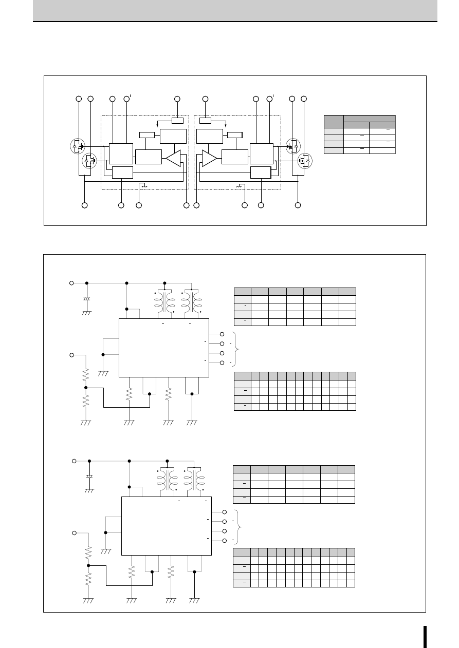
29
SLA7032M/SLA7033M
SLA7032M/SLA7033M
2-Phase Stepper Motor Unipolar Driver IC (2-Phase/1-2 Phase Excitation)
Rs
Rs
9
6
5
17
16
7
2
13
8
18
Active
Low
11
1
12
3
4
14
15
10
r1
r2
Vb (5V)
Vcc (46Vmax)
RsA
GA
GB
RsB
R
EF
A R
EF
B
OUT
A
SLA7032M
SLA7033M
VsA
VsB
OUT
A
IN
A
IN
A
IN
B
IN
B
OUT
B
OUT
B
IN
A
IN
A
IN
B
IN
B
+
SYNC A
SYNC B
Active Low
■
Internal Block Diagram
■
Diagram of Standard External Circuit (Recommended Circuit Constants)
Active High
+
−
1, 8, 11, 18pin
Description of pins
9
2
4
3
14
15
13
10
Chopping
blanking timer
(5 s typ)
Synchronous
chopping
circuit
Synchronous
chopping
circuit
MOSFET
gate drive
circuit
MOSFET
gate drive
circuit
IN A
IN A
IN B
IN B
Vs A
Vs B
Rs A
SYNC A
SYNC B
G A
R
EF
A
R
EF
B
G B
Oscillator
Oscillator
Reg.
Reg.
Rs B
+
−
Excitation input
Active H
OUT A
OUT A
OUT B
OUT B
1pin
8pin
11pin
18pin
Active L
OUT A
OUT A
OUT B
OUT B
5
6
7
17
8
1
16
11
18
12
Chopping
OFF timer
(12 s typ)
µ
Chopping
blanking timer
(5 s typ)
µ
µ
Chopping
OFF timer
(12 s typ)
µ
Rs
Rs
9
6
5
17
16
7
2
13
8
18
Active
High
11
1
12
3
4
14
15
10
r1
r2
Vb (5V)
Vcc (46Vmax)
RsA
GA
GB
RsB
R
EF
A R
EF
B
OUT
A
SLA7032M
SLA7033M
VsA
VsB
OUT
A
IN
A
IN
A
IN
B
IN
B
OUT
B
OUT
B
IN
A
IN
A
IN
B
IN
B
+
SYNC A
SYNC B
(1 to 2W)
r
1
: 4k
Ω
r
2
: 1k
Ω
(VR)
R
s
: 1
Ω
typ(7032M)
0.68
Ω
typ(7033M)
r
1
: 4k
Ω
r
2
: 1k
Ω
(VR)
R
s
: 1
Ω
typ(7032M)
0.68
Ω
typ(7033M)
1-2 phase excitation
clock
0
1
2
3
4
5
6
7
0
1
2
3
IN
A
H H L
L
L
L
L
H H H
L
L
IN
A
L
L
L
H H H
L
L
L
L
L
H
IN
B
L
H H H
L
L
L
L
L
H H H
IN
B
L
L
L
L
L
H H H L
L
L
L
Excitation signal time chart
2-phase excitation
clock
0
1
2
3
0
1
IN
A
H
L
L
H
H
L
IN
A
L
H
H
L
L
H
IN
B
H
H
L
L
H
H
IN
B
L
L
H
H
L
L
Excitation signal time chart
2-phase excitation
clock
0
1
2
3
0
1
IN
A
L
H
H
L
L
H
IN
A
H
L
L
H
H
L
IN
B
L
L
H
H
L
L
IN
B
H
H
L
L
H
H
1-2 phase excitation
clock
0
1
2
3
4
5
6
7
0
1
2
3
IN
A
L
L
H H H H H L
L
L
H H
IN
A
H H H
L
L
L
H H H H H
L
IN
B
H
L
L
L
H H H H H
L
L
L
IN
B
H H H H H
L
L
L
H H H H
(1 to 2W)
ac/Allegro/Allegro_Motor_Drive_ICs-html.html

30
SLA7032M/SLA7033M
SLA7032M/SLA7033M
2-Phase Stepper Motor Unipolar Driver IC (2-Phase/1-2 Phase Excitation)
■
External Dimensions
(Unit: mm)
31
±
0.2
24.4
±
0.2
16.4
±
0.2
3.2
±
0.15
φ
16
±
0.2
13
±
0.2
9.9
±
0.2
Part No.
Lot No.
3.2
±
0.15
×
3.8
φ
4.8
±
0.2
1.7
±
0.1
2.45
±
0.2
R-End
6.7
±
0.5
9.7
+1 –
0.5
(3)
0.55
+0.2
–0.1
4
±
0.7
1
+0.2
–0.1
17
×
P1.68
±
0.4
=28.56
±
1
0.65
+0.2
–0.1
31.3
±
0.2
Forming No. No.871
Forming No. No.872
1 2 3 · · · · · · · 18
123 · · · · · · · 18
17
×
P1.68
±
0.4
=28.56
±
1
0.65
+0.2
–0.1
1
+0.2
–0.1
3
±
0.6
0.55
+0.2 –
0.1
2.2
±
0.6
6
±
0.6
7.5
±
0.6
4.6
±
0.6
1.6
±
0.6
3.
4.
5.
ac/Allegro/Allegro_Motor_Drive_ICs-html.html
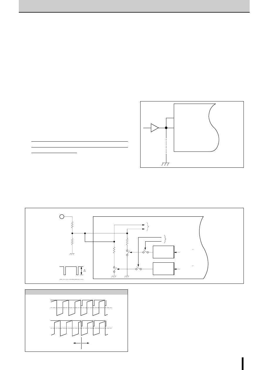
31
SLA7032M/SLA7033M
SLA7032M/SLA7033M
2-Phase Stepper Motor Unipolar Driver IC (2-Phase/1-2 Phase Excitation)
■
Outline
SLA7032M (SLA7033M) is a stepper motor driver IC developed
to reduce the number of external parts required by the conven-
tional SLA7024M (SLA7026M). This IC successfully eliminates
the need for some external parts without sacrificing the features
of SLA7024M (SLA7026M). The basic function pins are com-
patible with those of SLA7024M (SLA7026M).
■
Notes on Replacing SLA7024M (SLA7026M)
SLA7032M (SLA7033M) is pin-compatible with SLA7024M
(SLA7026M). When using the IC on an existing board, the fol-
lowing preparations are necessary:
(1) Remove the resistors and capacitors attached for setting
the chopping OFF time. (r
3
, r
4
, C
1
, and C
2
in the catalog)
(2) Remove the resistors and capacitors attached for preventing
noise in the detection voltage V
RS
from causing malfunction-
ing and short the sections from which the resistors were re-
moved using jumper wires. (r
5
, r
6
, C
3
, and C
4
in the catalog)
(3) Normally, keep pins 2 and 13 grounded because their func-
tions have changed to synchronous and asynchronous
switching (SYNC terminals). For details, see "Circuit for Pre-
venting Abnormal Noise When the Motor Is Not Running (Syn-
chronous circuit)." (Low: asynchronous, High: synchronous)
■
Circuit for Preventing Abnormal Noise When the
Motor Is Not Running (Synchronous Circuit)
A motor may generate abnormal noise when it is not running. This
phenomenon is attributable to asynchronous chopping between
phases A and B. To prevent the phenomenon, SLA7032M
(SLA7033M) contains a synchronous chopping circuit. Do not leave
Synchronous circuit operating waveform
SYNC_A
SYNC voltage : Low
SYNC voltage : High
→
Chopping asynchronous
→
Chopping synchronous
TTL, etc.
SYNC_B
SLA7032M
SLA7033M
Sync/async switching
signal
To comparator
(high impedance)
REF_A
R1
R2
3
5V
REF_B
V
REF
V
REF
waveform
V
REF
0
14
SLA7032M
SLA7033M
FET A/A
gate drive signal
40
Ω
(typ.)
40
Ω
(typ.)
FET B/B
gate drive signal
ONE SHOT
(tw=2 S)
µ
ONE SHOT
(tw=2 S)
µ
V
REF
V
RS
Phase A
0
V
REF
V
RS
Synchronous circuit ON
Synchronous circuit OFF
Phase B
0
Application Notes
the SYNC terminals open because they are for CMOS input.
Connect TTL or similar to the SYNC terminals and switch the
SYNC terminal level high or low.
When the motor is not running, set the TTL signal high (SYNC
terminal voltage: 4 V or more) to make chopping synchronous.
When the motor is running, set the TTL signal low (SYNC terminal
voltage: 0.8 V or less) to make chopping asynchronous. If chop-
ping is set to synchronous at when the motor is running, the motor
torque deteriorates before the coil current reaches the set value.
If no abnormal noise occurs when the motor is not running,
ground the SYNC terminals (TTL not necessary).
The built-in synchronous chopping circuit superimposes a trigger
signal on the REF terminal for synchronization between the two
phases. The figure below shows the internal circuit of the REF
terminal. Since the
∆
V
REF
varies depending on the values of R1
and R2, determine these values for when the motor is not run-
ning within the range where the two phases are synchronized.
ac/Allegro/Allegro_Motor_Drive_ICs-html.html
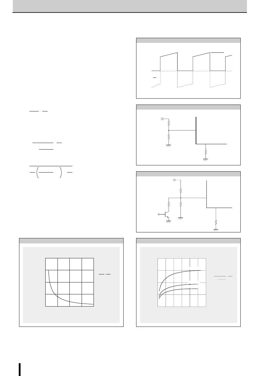
32
SLA7032M/SLA7033M
SLA7032M/SLA7033M
2-Phase Stepper Motor Unipolar Driver IC (2-Phase/1-2 Phase Excitation)
R
S
r
2
r
1
V
b
(5
V
)
9,(10)
3,(14)
r
2
r
1
V
b
(5
V
)
9,(10)
3,(14)
r
X
T
r
Power down
signal
■
Determining the Output Current
Fig. 1 shows the waveform of the output current (motor coil cur-
rent). The method of determining the peak value of the output
current (I
O
) based on this waveform is shown below.
(Parameters for determining the output current I
O
)
V
b
: Reference supply voltage
r
1
,r
2
: Voltage-divider resistors for the reference supply voltage
R
S
: Current sense resistor
(1) Normal rotation mode
I
O
is determined as follows when current flows at the maximum
level during motor rotation. (See Fig.2.)
(2) Power down mode
The circuit in Fig.3 (r
x
and T
r
) is added in order to decrease the
coil current. I
O
is then determined as follows.
Equation (2) can be modified to obtain equation to determine r
x
.
Fig. 4 and 5 show th e graphs of equations (1) and (2) respec-
tively.
Fig. 2 Normal mode
0
Phase A
Phase A
I
O
Fig. 1 Waveform of coil current (Phase A excitation ON)
Fig. 3 Power down mode
4
3
2
1
0
0
1
2
3
4
Current sense resistor R
S
(
Ω
)
Output current I
O
(A)
I
O
=
r
1
+r
2
R
S
r
1
=510
Ω
r
2
=100
Ω
r
x
=
∞
V
b
=5V
r
2
·
V
b
Fig. 4 Output current I
O
vs. Current sense resistor R
S
Fig. 5 Output current I
OPD
vs. Variable current sense resistor r
x
2.0
1.5
1.0
0.5
00
200
400
600
800
Variable current sense resistor r
X
(
Ω
)
Output current I
OPD
(A)
1000
1200
R
S
=0.5
Ω
R
S
=0.8
Ω
R
S
=1
Ω
I
OPD
=
1+ R
S
r
1
=510
Ω
r
2
=100
Ω
V
b
=5V
1
·
V
b
r
1
(r
2+
r
X
)
r
2 ·
r
X
r
X
=
1
V
b
R
s
•
I
OPD
1
r
1
−
1
−
1
r
2
................................................................ (1)
I
O
≅
•
r
2
r
1
+r
2
V
b
R
S
......................................................... (2)
I
OPD
≅
•
1
r
1
(r
2
+r
X
)
r
2
•
r
X
V
b
R
S
1+
ac/Allegro/Allegro_Motor_Drive_ICs-html.html
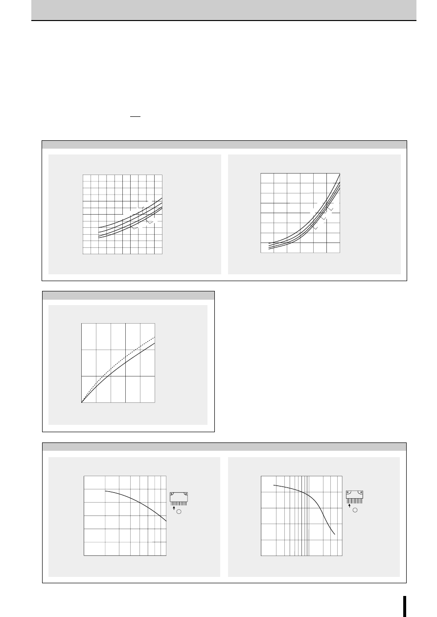
33
SLA7032M/SLA7033M
SLA7032M/SLA7033M
2-Phase Stepper Motor Unipolar Driver IC (2-Phase/1-2 Phase Excitation)
50
40
30
20
10
0
100
500
1K
5K
Case temper
ature r
ise
∆
T
C
–
a
(
°
C)
Response frequency (pps)
Without heatsink
Natural cooling
Motor : 23PM-C705
Motor current I
O
=1.5A
T
a
=25
°
C
V
CC
=24V, V
S
=24V
2-phase excitation
T
C
( 4 pin)
30
25
20
15
10
5
0
200
500
1K
Case temperature rise
∆
T
C
–
a
(
°
C)
Motor : PH265-01B
Motor current I
O
=0.8A
T
a
=25
°
C
V
CC
=24V, V
S
=24V
2-phase excitation
Response frequency (pps)
Without heatsink
Natural cooling
T
C
( 4 pin)
SLA7032M
SLA7033M
Thermal characteristics
Fig. 7 Temperature rise
Fig. 6 Heat dissipation per phase P
H
vs. Output current I
O
Output current I
O
(A)
Heat dissipation per phase P
H
(W)
Motor : 23LM-C004
Holding mode
0
0.2
0.4
0.6
0.8
1.0
1.2
1.0
0.8
0.6
0.4
0.2
0
V
CC
=44V
36V
24V
15V
∆
T
j–
a
∆
T
C
–
a
∆
T
j
1
0
2
3
4
5
∆
T
C
Natural cooling
Without heatsink
150
100
50
0
Total Power (W)
(
°
C)
Heat dissipation per phase P
H
(W)
Motor : 23PM-C503
Holding mode
36V
15V
24V
V
CC
=44V
4.0
3.0
2.0
1.0
0
0
1.0
2.0
3.0
Output current I
O
(A)
SLA7032M
SLA7033M
■
Thermal Design
An outline of the method for calculated heat dissipation is shown below.
(1) Obtain the value of P
H
that corresponds to the motor coil current I
O
from Fig. 6 "Heat dissipation per phase P
H
vs. Output current I
O
."
(2) The power dissipation P
diss
is obtained using the following formula.
2-phase excitation: P
diss
≅
2P
H
+0.015
×
V
S
(W)
1-2 phase excitation: P
diss
≅
P
H
+0.015
×
V
S
(W)
(3) Obtain the temperature rise that corresponds to the computed value of P
diss
from Fig. 7 "Temperature rise."
3
2
ac/Allegro/Allegro_Motor_Drive_ICs-html.html
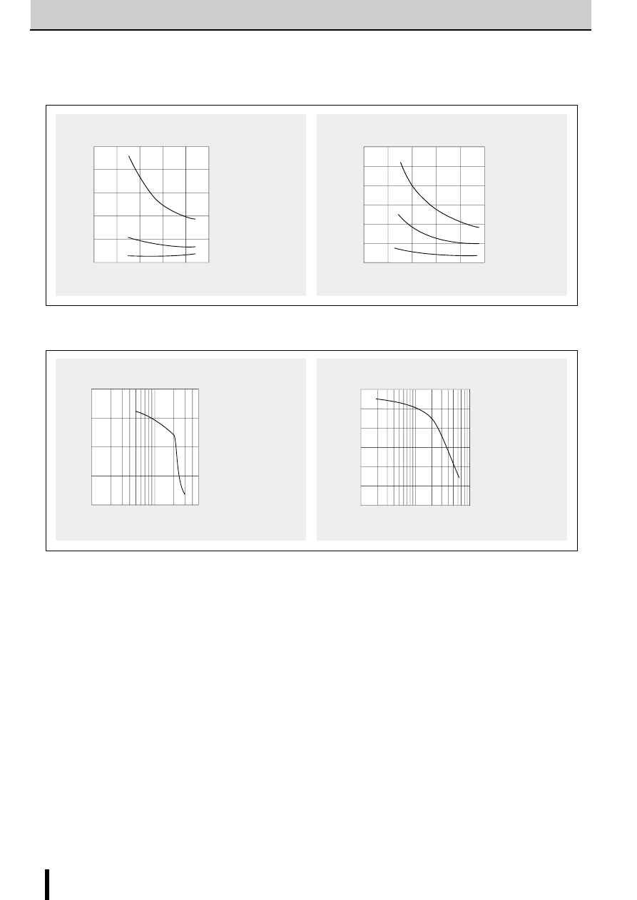
34
SLA7032M/SLA7033M
SLA7032M/SLA7033M
2-Phase Stepper Motor Unipolar Driver IC (2-Phase/1-2 Phase Excitation)
■
Supply Voltage V
CC
vs. Supply Current I
CC
0
Supply current I
CC
(mA)
Supply voltage V
CC
(V)
500
400
300
200
100
0
10
20
30
40
50
0.2A
0.5A
I
O
=1A
Motor : 23LM-C004
1-phase excitation
Holding mode
I
O
: Output current
■
Torque Characteristics
100
Pull-out torque (kg-cm)
Response frequency (pps)
2.0
1.5
1.0
0.5
0
5K
1K
500
Motor : 23LM-C202
Output current I
O
=0.8A
Motor supply voltage V
CC
=24V
2-phase excitation
0
Supply current I
CC
(A)
Supply voltage V
CC
(V)
1.5
1.0
0.5
0
10
20
30
40
50
Motor : 23PM-C503
1-phase excitation
Holding mode
I
O
: Output current
I
O
=1A
I
O
=2A
I
O
=3A
100
Pull-out torque (kg-cm)
Response frequency (pps)
6.0
5.0
4.0
3.0
2.0
1.0
0
5K
10K
1K
500
Motor : 23PM-C705
Output current I
O
=2.5A
Motor supply voltage V
CC
=24V
2-phase excitation
SLA7032M
SLA7033M
SLA7032M
SLA7033M
ac/Allegro/Allegro_Motor_Drive_ICs-html.html

35
SLA7032M/SLA7033M
SLA7032M/SLA7033M
2-Phase Stepper Motor Unipolar Driver IC (2-Phase/1-2 Phase Excitation)
■
Handling Precautions
The input terminals of this product use C-MOS circuits. Observe the following precautions.
●
Carefully control the humidity of the room to prevent the buildup of static electricity. Since static electricity is particularly a problem
during the winter, be sure to take sufficient precautions.
●
Take care to make sure that static electricity is not applied to the IC during wiring and assembly. Take precautions such as shorting
the terminals of the printed wiring board to ensure that they are at the same electrical potential.
Active Low
Input
Corresponding output
IN
A
(pin6)
OUT
A
(pin8)
IN
A
(pin5)
OUT
A
(pin1)
IN
B
(pin17)
OUT
B
(pin18)
IN
B
(pin16)
OUT
B
(pin11)
Active High
Input
Corresponding output
IN
A
(pin6)
OUT
A
(pin1)
IN
A
(pin5)
OUT
A
(pin8)
IN
B
(pin17)
OUT
B
(pin11)
IN
B
(pin16)
OUT
B
(pin18)
■
Note
The excitation input signals of the SLA7032M, SLA7033M can be used as either Active High or Active Low. Note, however, that the
corresponding output (OUT) changes depending on the input (IN).
■
Chopper frequency vs. Supply voltage
0
f (kHz)
V
CC
(V)
50
40
30
20
10
0
10
20
30
40
50
Motor : 23LM-C202
I
O
= 0.8A at V
CC
=24V
R
S
=1
Ω
■
Chopper frequency vs. Output current
0
f (kHz)
I
O
(A)
50
40
30
20
10
0
0.2
0.4
0.6
0.8
1.0
Motor : 23LM-C202
V
CC
=24V
R
S
=1
Ω
ac/Allegro/Allegro_Motor_Drive_ICs-html.html

36
SDK03M
2-Phase Stepper Motor Unipolar Driver ICs
SDK03M
■
Electrical Characteristics
■
Absolute Maximum Ratings
Parameter
Symbol
Ratings
Units
min
typ
max
Control supply current
I
S
5
7.5
mA
Condition
V
S
=44V
Control supply voltage
V
S
10
24
44
V
FET Drain-Source
V
DSS
100
V
voltage
Condition
V
S
=44V, I
DSS
=250
µ
A
FET ON voltage
V
DS
0.85
V
Condition
I
D
=1A, V
S
=14V
FET drain leakage current
I
DSS
4
mA
Condition
V
DSS
=100V, V
S
=44V
FET diode forward
V
SD
1.2
V
voltage
Condition
I
D
=1A
I
IH
40
µ
A
TTL input current
Condition
V
IH
=2.4V, V
S
=44V
I
IL
−
0.8
mA
Condition
V
IL
=0.4V, V
S
=44V
V
IH
2
TTL input voltage
Condition
I
D
=1A
V
(Active High)
V
IL
0.8
Condition
V
DSS
=100V
V
IH
2
TTL input voltage
Condition
V
DSS
=100V
V
(Active Low)
V
IL
0.8
Condition
I
D
=1A
T
r
0.5
Condition
V
S
=24V, I
D
=0.8A
Switching time
T
stg
0.7
µ
s
Condition
V
S
=24V, I
D
=0.8A
T
f
0.1
Condition
V
S
=24V, I
D
=0.8A
Parameter
Symbol
Ratings
Units
Motor supply voltage
V
CC
46
V
FET Drain-Source voltage
V
DSS
100
V
Control supply voltage
V
S
46
V
TTL input voltage
V
IN
7
V
Reference voltage
V
REF
2
V
Output current
I
O
1
A
Power dissipation
P
D
2.5 (Without Heatsink)
W
Channel temperature
T
ch
+150
°
C
Storage temperature
T
stg
−
40 to +150
°
C
2-Phase/1-2 Phase Excitation
DC characteristics
AC characteristics
ac/Allegro/Allegro_Motor_Drive_ICs-html.html
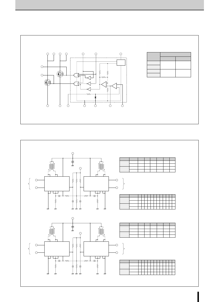
37
SDK03M
SDK03M
2-Phase Stepper Motor Unipolar Driver ICs (2-Phase/1-2 Phase Excitation)
■
Internal Block Diagram
■
Diagram of Standard External Circuit (Recommended Circuit Constants)
Excitation input
Active H
Active L
Pin 1
OUT
1
OUT
2
Pin 16
Pin 8
OUT
2
OUT
1
Pin 9
8
Reg.
2
3
12
1
6
10
5
7
+
–
+
–
15
13
4
16
9
IN
1
IN
2
V
S
14
11
NC
NC
R
S
R
S
R
S
GND
GND
REF
T
D
Active High
Active Low
+
V
CC
(46V max)
Motor coil
Phase A
Motor coil
Phase B
Motor coil
Phase A
Motor coil
Phase B
V
b
(5V)
1
16
8
9
7
6
5
IN
1
IN
2
12
10
15
13
3
C
3
r
5
R
S
4
C
1
C
2
r
2
r
6
C
4
R
S
OUT
1
OUT
2
V
S
GND
R
S
REF
T
D
IN
1
IN
2
2
r
3
r
1
r
4
2
SDK03M
Phase A
12
10
4
IN
1
IN
2
IN
1
IN
2
6
5
V
S
OUT
2
OUT
1
REF
R
S
GND
T
D
SDK03M
Phase B
7
1
16
8
9
3
13
15
Active
High
Active
High
+
V
CC
(46V max)
V
b
(5V)
1
16
8
9
7
6
5
IN
1
IN
2
12
10
15
13
3
C
3
r
5
R
S
4
C
1
C
2
r
2
r
6
C
4
R
S
OUT
2
OUT
1
V
S
GND
R
S
REF
T
D
IN
1
IN
2
2
r
3
r
1
r
4
2
SDK03M
Phase A
12
10
4
IN
1
IN
2
IN
1
IN
2
6
5
V
S
OUT
1
OUT
2
REF
R
S
GND
T
D
SDK03M
Phase B
7
1
16
8
9
3
13
15
Active
Low
Active
Low
1, 8, 9, 16pin Description of pins
Excitation signal time chart
2-phase excitation
Phase
clock
0
1
2
3
0
1
Phase A
IN
1
H
L
L
H
H
L
IN
2
L
H
H
L
L
H
Phase B
IN
1
H
H
L
L
H
H
IN
2
L
L
H
H
L
L
1-2-phase excitation
Phase
clock
0 1 2 3 4 5 6 7 0 1 2 3
Phase A
IN
1
H H L L L L L H H H L L
IN
2
L L L H H H L L L L L H
Phase B
IN
1
L H H H L L L L L H H H
IN
2
L L L L L H H H L L L L
Excitation signal time chart
2-phase excitation
Phase
clock
0
1
2
3
0
1
Phase A
IN
1
L
H
H
L
L
H
IN
2
H
L
L
H
H
L
Phase B
IN
1
L
L
H
H
L
L
IN
2
H
H
L
L
H
H
1-2-phase excitation
Phase
clock
0 1 2 3 4 5 6 7 0 1 2 3
Phase A
IN
1
L L H H H H H L L L H H
IN
2
H H H L L L H H H H H L
Phase B
IN
1
H L L L H H H H H L L L
IN
2
H H H H H L L L H H H H
r
1
:
510
Ω
r
2
:
100
Ω
(VR)
r
3
:
47k
Ω
r
4
:
47k
Ω
r
5
:
2.4k
Ω
r
6
:
2.4k
Ω
C
1 :
470pF
C
2 :
470pF
C
3 :
2200pF
C
4 :
2200pF
R
S
:
1.8
Ω
typ
r
1
:
510
Ω
r
2
:
100
Ω
(VR)
r
3
:
47k
Ω
r
4
:
47k
Ω
r
5
:
2.4k
Ω
r
6
:
2.4k
Ω
C
1 :
470pF
C
2 :
470pF
C
3 :
2200pF
C
4 :
2200pF
R
S
:
1.8
Ω
typ
(1 to 2W)
(1 to 2W)
ac/Allegro/Allegro_Motor_Drive_ICs-html.html
38
SDK03M
SDK03M
2-Phase Stepper Motor Unipolar Driver ICs (2-Phase/1-2 Phase Excitation)
■
External Dimensions
(Unit: mm)
Part No.
Lot No.
2.54
±
0.25
0.75
+0.15
–0.05
0.89
±
0.15
16
6.8
max.
20.0
max.
19.56
±
0.2
9
8
1
4.0
max.
3.6
±
0.2
1.4
±
0.2
0.3
+0.15 –
0.05
8.0
±
0.5
6.3
±
0.2
3.0
±
0.2
0~0.1
1.0
±
0.3
9.8
±
0.3
0.25
ac/Allegro/Allegro_Motor_Drive_ICs-html.html
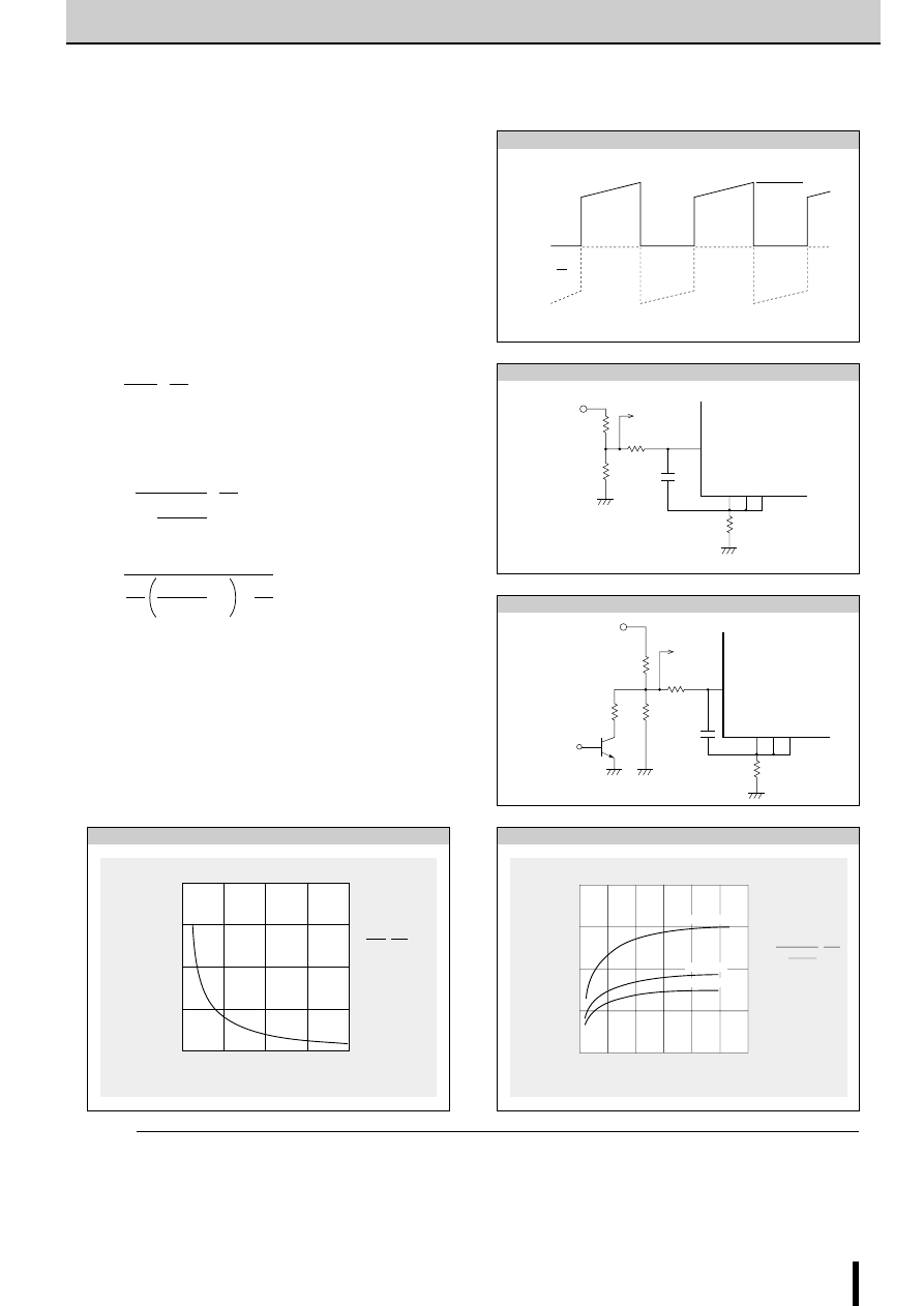
39
SDK03M
SDK03M
2-Phase Stepper Motor Unipolar Driver ICs (2-Phase/1-2 Phase Excitation)
R
S
C
3
r
2
r
1
r
6
r
5
V
b
(5
V
)
10
3
13 15
R
S
C
3
r
2
r
1
r
6
r
5
V
b
(5
V
)
10
3
r
X
T
r
Power down
signal
13 15
■
Determining the Output Current
Fig. 1 shows the waveform of the output current (motor coil cur-
rent). The method of determining the peak value of the output
current (I
O
) based on this waveform is shown below.
(Parameters for determining the output current I
O
)
V
b
: Reference supply voltage
r
1
,r
2
: Voltage-divider resistors for the reference supply voltage
R
S
: Current sense resistor
(1) Normal rotation mode
I
O
is determined as follows when current flows at the maximum
level during motor rotation. (See Fig.2.)
(2) Power down mode
The circuit in Fig.3 (r
x
and T
r
) is added in order to decrease the
coil current. I
O
is then determined as follows.
Equation (2) can be modified to obtain equation to determine r
x
.
Fig. 4 and 5 show the graphs of equations (1) and (2) respec-
tively.
Fig. 2 Normal mode
0
Phase A
Phase A
I
O
Fig. 1 Waveform of coil current (Phase A excitation ON)
Fig. 3 Power down mode
4
3
2
1
0
0
1
2
3
4
Current sense resistor R
S
(
Ω
)
Output current I
O
(A)
I
O
=
r
1
+r
2
R
S
r
1
=510
Ω
r
2
=100
Ω
r
x
=
∞
V
b
=5V
r
2
·
V
b
Fig. 4 Output current I
O
vs. Current sense resistor R
S
Fig. 5 Output current I
OPD
vs. Variable current sense resistor r
x
2.0
1.5
1.0
0.5
00
200
400
600
800
Variable current sense resistor r
X
(
Ω
)
Output current I
OPD
(A)
1000
1200
R
S
=0.5
Ω
R
S
=0.8
Ω
R
S
=1
Ω
I
OPD
=
1+ R
S
r
1
=510
Ω
r
2
=100
Ω
V
b
=5V
1
·
V
b
r
1
(r
2+
r
X
)
r
2 ·
r
X
Application Notes
r
X
=
1
V
b
R
s
•
I
OPD
1
r
1
−
1
−
1
r
2
(NOTE)
Ringing noise is produced in the current sense resistor R
S
when
the MOSFET is switched ON and OFF by chopping. This noise
is also generated in feedback signals from R
S
which may there-
fore cause the comparator to malfunction. To prevent chopping
malfunctions, r
5
(r
6
) and C
3
(C
4
) are added to act as a noise filter.
However, when the values of these constants are increased,
the response from R
S
to the comparator becomes slow. Hence
the value of the output current I
O
is somewhat higher than the
calculated value.
................................................................ (1)
I
O
≅
•
r
2
r
1
+r
2
V
b
R
S
......................................................... (2)
I
OPD
≅
•
1
r
1
(r
2
+r
X
)
r
2
•
r
X
V
b
R
S
1+
ac/Allegro/Allegro_Motor_Drive_ICs-html.html
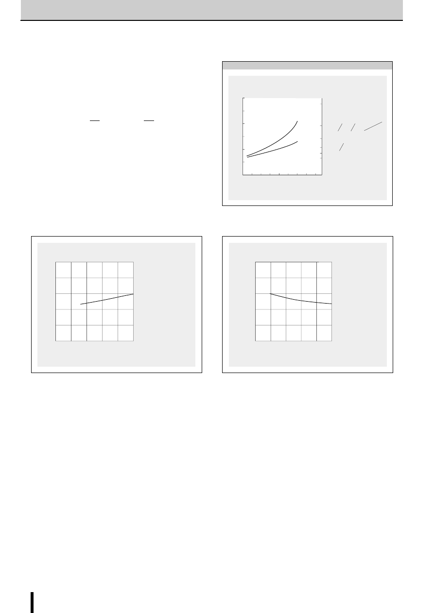
40
SDK03M
SDK03M
2-Phase Stepper Motor Unipolar Driver ICs (2-Phase/1-2 Phase Excitation)
60
50
40
30
20
10
0
0
2
4
6
8
10 12
14
16
15
20
25
30
35
40
Motor coil resistance R
m
(
Ω
)
ON time T
ON
( s)
V
CC
=2
4V
V
CC
=36V
Chopping frequency f (kHz)
T
OFF
=12 s
R
S
=1
Ω
L
m
=1~3ms
R
m
= =
r
3
C
1
r
4
C
2
47k
Ω
500pF
µ
µ
Fig. 6 Chopper frequency vs. Motor coil resistance
■
Determining the chopper frequency
Determining T
OFF
SDK03M is self-excited choppers. The chopping OFF time T
OFF
is fixed by r
3
/C
1
and r
4
/C
2
connected to terminal T
d
.
T
OFF
can be calculated using the following formula:
The circuit constants and the T
OFF
value shown below are rec-
ommended.
T
OFF
= 12
µ
s at r
3
=47k
Ω
, C
1
=500pF, V
b
=5V
■
Chopper frequency vs. Supply voltage
■
Chopper frequency vs. Output current
0
f (kHz)
V
CC
(V)
50
40
30
20
10
0
10
20
30
40
50
Motor : 23LM-C202
I
O
= 0.8A at V
CC
=24V
R
S
=1
Ω
0
f (kHz)
I
O
(A)
50
40
30
20
10
0
0.2
0.4
0.6
0.8
1.0
Motor : 23LM-C202
V
CC
=24V
R
S
=1
Ω
T
OFF
≅−
r
3
•
C
1 n
(1
−
=
−
r
4
•
C
2
n
(1
−
)
r
r
2
V
b
2
V
b
ac/Allegro/Allegro_Motor_Drive_ICs-html.html
41
SDK03M
SDK03M
2-Phase Stepper Motor Unipolar Driver ICs (2-Phase/1-2 Phase Excitation)
■
Supply Voltage V
CC
vs. Supply Current I
CC
■
Torque Characteristics
0
Supply current I
CC
(mA)
Supply voltage V
CC
(V)
500
400
300
200
100
0
10
20
30
40
50
Motor : 23LM-C202
1-phase excitation
Holding mode
I
O
: Output current
I
O
=1A
0.4A
0.2A
100
Pull-out torque (kg-cm)
Response frequency (pps)
2.0
1.5
1.0
0.5
0
5K
1K
500
Motor : PX244-02
Output current I
O
=0.6A
Motor supply voltage V
CC
=24V
2-phase excitation
1.2
1
0.8
0.6
0.4
0.2
0
0
0.2
0.4
0.6
0.8
1.0
Heat dissipation per phase P
H
(W)
Output current I
O
(A)
36V
24V
15V
V
CC
=44V
Motor : 23LM-C202
Holding mode
Fig. 7 Heat dissipation per phase P
H
vs. Output current I
O
∆
T
j
1
0
2
3
∆
T
C
Glass epoxy board
(mounted on level surface)
(95
×
69
×
1.2mm)
Natural cooling
150
100
50
0
Total power (W)
∆
T
j–
a
∆
T
C
–
a
(
°
C)
50
40
30
20
10
0
200
500
1K
Case temperature rise
∆
T
C
–
a
(
°
C)
Response frequency (pps)
T
C
( 9 pin)
Natural cooling
Glass epoxy board
(mounted on level surface)
(95
×
69
×
1.2mm)
Motor : PH265-01B
Motor current I
O
=0.8A
T
a
=25
°
C
V
CC
=24V, V
S
=24V
2-phase excitation
Thermal characteristics
Fig. 8 Temperature rise
Active Low
Input
Corresponding output
IN
1
(pin6)
OUT
1
(pin8, 9)
IN
2
(pin5)
OUT
2
(pin1, 16)
Active High
Input
Corresponding output
IN
1
(pin6)
OUT
1
(pin1, 16)
IN
2
(pin5)
OUT
2
(pin8, 9)
■
Note
The excitation input signals of the SDK03M can be used as either Active High or Active Low. Note, However, that the corresponding
output (OUT) changes depending on the input (IN).
■
Thermal Design
An outline of the method for computing heat dissipation is shown below.
(1) Obtain the value of P
H
that corresponds to the motor coil current
I
O
from Fig. 7 "Heat dissipation per phase P
H
vs. Output current
I
O
."
(2) The power dissipation Pdiss is obtained using the following formula.
2-phase excitation: P
diss
≅
P
H
+0.0075
×
V
S
(W)
1-2 phase excitation: P
diss
≅
P
H
+0.0075
×
V
S
(W)
(3) Obtain the temperature rise that corresponds to the calcu-
lated value of P
diss
from Fig. 8 "Temperature rise."
3
4
ac/Allegro/Allegro_Motor_Drive_ICs-html.html
42
UCN5804B
2-Phase Stepper Motor Unipolar Driver IC
UCN5804B
Allegro MicroSystems product
■
Features
●
Internal 1-phase/1-2 phase/2-phase excita-
tion pattern generator
●
Output enable and direction control
●
Power-on reset
●
Internal thermal shutdown circuitry
●
Internal transient-suppression diodes
●
Low thermal resistance 16-pin DIP
■
Electrical Characteristics
Parameter
Symbol
Conditions
Limits
Units
min
typ
max
Output drivers
Output leakage current
I
CEX
V
O
=50V
10
50
µ
A
Output sustaining voltage
V
CE (SUS)
I
O
=1.25A, L=3mH
3.5
V
I
O
=700mA
1.0
1.2
V
Output saturation voltage
V
CE (SAT)
I
O
=1A
1.1
1.4
V
I
O
=1.25A
1.2
1.5
V
Clamp diode leakage current
I
R
V
R
=50V
10
50
µ
A
Clamp diode forward voltage
V
F
I
F
=1.25A
1.5
3.0
V
Turn-on delay
t
ON
50% step inputs to 50% output
10
µ
s
Turn-off delay
t
OFF
50% step inputs to 50% output
10
µ
s
Thermal shutdown temperature
T
j
165
°
C
Control logic
Input current
I
IH
V
IN
=V
DD
0.5
5.0
µ
A
I
IL
V
IN
=0.8V
−
0.5
−
5.0
µ
A
Input voltage
V
IH
V
DD
=5V
3.5
5.3
V
V
IL
−
0.3
0.8
V
Supply current
I
DD
2 outputs ON
20
30
mA
Data setup time
t
s DAT (A)
Inter-clock
100
ns
Data hold time
t
h DAT (B)
Inter-clock
100
ns
Clock pulse width
t
w CLK (C)
500
ns
●
"typ" values are for reference.
Absolute Maximum Ratings
Parameter
Symbol
Ratings
Units
Output voltage
V
CE
50
V
Output sustaining voltage
V
CE (SUS)
35
V
Output current (1 circuit)
I
O
1.5
A/unit
Logic supply voltage
V
DD
7.0
V
Input voltage
V
IN
7.0
V
Package power dissipation
P
D
(Note1)
2.90
W/pkg
Operating temperature
T
a
−
20 to +85
°
C
Junction temperature
T
j
(Note2)
+150
°
C
Storage temperature
T
stg
−
55 to +150
°
C
Note 1: When ambient temperature is 25
°
C or over, derate using
−
23.3mW/
°
C.
Note 2: Fault conditions where junction temperature (T
j
) exceeds 150
°
C will activate the device's thermal
shutdown circuitry. These conditions can be tolerated but should be avoided.
(Unless specified otherwise, T
a
=25
°
C, V
DD
=4.5V to 5.5V)
(T
a
=+25
°
C)
(Unless specified otherwise, V
IN
=V
DD
or GND)
■
Terminal Connection Diagram
■
Timing Conditions
1
2
3
4
5
6
7
8
9
10
11
12
13
14
15
16
OUTPUT
B
OUTPUT
D
OUTPUT
C
OUTPUT
A
GROUND
GROUND
SUPPLY
DIRECTION
OUTPUT
ENABLE
OE
GROUND
HALF-STEP
ONE-PHASE
STEP INPUT
GROUND
K
BD
V
DD
K
AC
LOGIC
CLOCK
ONE PHASE
HALF-STEP
OUTPUT
A
OUTPUT
B
OUTPUT
C
OUTPUT
D
OUTPUT
ENABLE
C
A
B
TWO-PHASE
HALF-STEP
OUTPUT
DISABLED
WAVE DRIVE
2-Phase/1-2 Phase Excitation
ac/Allegro/Allegro_Motor_Drive_ICs-html.html
43
UCN5804B
2-Phase Stepper Motor Unipolar Driver IC (2-Phase/1-2 Phase Excitation)
UCN5804B
■
Derating
■
Application Circuit
■
I/O Equivalent Circuit
■
Truth Table
IN
V
DD
SUB
Input circuit
Output driver
■
External Dimensions
4
5
3
2
1
0
−
20
0
25
50
75
100
85
43
°
C/
W
Ambient temperature Ta (
°
C)
Allowable package power dissipationP
D
(W)
K
OUT
Drive Format
Pin 9
Pin 10
Two-Phase
L
L
One-Phase
H
L
Half-Step
L
H
Step-Inhibit
H
H
1.77
1
2
3
8
9
16
1.15
21.33
18.93
0.558
0.356
4.06
2.93
7.11
6.10
INDEX AREA
0.127MIN
7.62BSC
2.54BSC
5.33MAX
SEATING PLANE
0.39MIN
0.508
0.204
Note 1
●
Thickness of lead is measured below seating plane.
●
Allowable variation in distance between leads is not cumulative.
Note 1: Lead width of pin 1,8, 9, 16 may be half the value shown here.
1
2
3
4
5
6
7
8
9
10
11
12
13
14
15
16
DIRECTION
CONTROL
OE
STEP INPUT
V
DD
LOGIC
1
2
3
4
5
6
7
8
9
10
11
12
13
14
15
16
OE
V
DD
LOGIC
5V
28V
OR
ICs per stick
25
(Unit: mm)
ac/Allegro/Allegro_Motor_Drive_ICs-html.html
44
SLA7042M/SLA7044M
2-Phase Stepper Motor Unipolar Driver ICs
SLA7042M/SLA7044M
Parameter
Symbol
Ratings
Units
SLA7042M
SLA7044M
Motor supply voltage
V
CC
46
V
FET Drain-Source voltage
V
DSS
100
V
Control supply voltage
V
DD
7
V
Input voltage
V
IN
−
0.5 to V
DD
+0.5
V
Output current
I
O
1.2
3
A
Power dissipation
P
D
4.5 (Without Heatsink)
W
Channel temperature
T
ch
+150
°
C
Storage temperature
T
stg
−
40 to +150
°
C
■
Absolute Maximum Ratings
■
Electrical Characteristics
Terminals
DATA,
CLOCK
and
STROBE
Ratings
Parameter
Symbol
SLA7042M
SLA7044M
Units
min
typ
max
min
typ
max
Control supply current
I
DD
7
7
mA
Conditions
V
DD
=5.5V
V
DD
=5.5V
Control supply voltage
V
DD
4.5
5
5.5
4.5
5
5.5
V
V
IH
3.5
5
3.5
5
Conditions
V
DD
=5V
V
DD
=5V
V
IL
0
1.5
0
1.5
V
Conditions
V
DD
=5V
V
DD
=5V
V
H
1
1
V
Conditions
V
DD
=5V
V
DD
=5V
I
I
±
1
±
1
µ
A
Conditions
V
DD
=5V, V
I
=0 or 5V
V
DD
=5V, V
I
=0 or 5V
V
REF
0.4
2.5
0.4
2.5
Conditions
V
DD
=5V
V
DD
=5V
V
REF
V
DISABLE
V
DD
−
1
V
DD
V
DD
−
1
V
DD
terminal
Conditions
V
DD
=5V
V
DD
=5V
I
REF
±
1
±
1
µ
A
Conditions
V
DD
=5V, V
I
=0 or 5V
V
DD
=5V, V
I
=0 or 5V
V
ref
0
0
Conditions
MODE 0
MODE 0
V
ref
20
20
Conditions
MODE 1
MODE 1
V
ref
40
40
Conditions
MODE 2
MODE 2
V
ref
55.5
55.5
Reference voltage
Conditions
MODE 3
MODE 3
%
selection output voltage
V
ref
71.4
71.4
Conditions
MODE 4
MODE 4
V
ref
83
83
Conditions
MODE 5
MODE 5
V
ref
91
91
Conditions
MODE 6
MODE 6
V
ref
100
100
Conditions
MODE 7
MODE 7
FET ON voltage
V
DS
0.8
1.4
V
Conditions
I
D
=1.2A, V
DD
=4.75V
I
D
=3A, V
DD
=4.75V
FET Drain-Source
V
DSS
100
100
V
voltage
Conditions
I
DSS
=4mA, V
DD
=5V
I
DSS
=4mA, V
DD
=5V
FET drain leakage current
I
DSS
4
4
mA
Conditions
V
DSS
=100V, V
DD
=5V
V
DSS
=100V, V
DD
=5V
FET diode forward voltage
V
SD
1.2
2.3
V
Conditions
I
D
=1.2A
I
D
=3A
T
OFF
7
7
Conditions
MODE 1, 2
MODE 1, 2
Chopper off time
T
OFF
9
9
µ
s
Conditions
MODE 3, 4, 5
MODE 3, 4, 5
T
OFF
11
11
Conditions
MODE 6, 7
MODE 6, 7
T
r
0.5
0.5
Conditions
V
DD
=5V, I
D
=1A
V
DD
=5V, I
D
=1A
Switching time
T
stg
0.7
0.7
µ
s
Conditions
V
DD
=5V, I
D
=1A
V
DD
=5V, I
D
=1A
T
f
0.1
0.1
Conditions
V
DD
=5V, I
D
=1A
V
DD
=5V, I
D
=1A
Data setup time "A"
ts
DAT
75
75
Conditions
Inter-clock
Inter-clock
Data hold time "B"
th
DAT
75
75
Conditions
Inter-clock
Inter-clock
Data pulse time "C"
tw
DAT
150
150
Conditions
ns
Clock pulse width "D"
twh
CLK
100
100
Conditions
Stabilization time
tps
STB
100
100
before strobe "E"
Conditions
Strobe=L from clock
Strobe=L from clock
Strobe pulse H width "F"
twh
STB
100
100
Conditions
2W1-2 Phase Excitation/Micro-step Support
Input
voltage
Input hysteresis
voltage
Input
current
Input
voltage
Input
current
DC characteristics
AC characteristics
ac/Allegro/Allegro_Motor_Drive_ICs-html.html
45
SLA7042M/SLA7044M
2-Phase Stepper Motor Unipolar Driver ICs (2W1-2 Phase Excitation/Micro-step Support)
SLA7042M/SLA7044M
■
Internal Block Diagram
■
Diagram of Standard External Circuit
■
Output Current Formula
K: Reference voltage setting rate by serial signal
(See the internal block diagram)
I
O
=
•
K
V
REF
3 R
S
V
DD
A
V
DD
B OUT A
OUT A OUT B
OUT B
REF A
REF B
GND A GND B
RS A
RS B
7
12
9
10
R
S
R
S
R
2
C
1
3
14
V
REF
R
1
5V
ENABLE
4
15
1
8
11
18
5
16
2
13
6
17
CLOCK A
CLOCK B
STROBE A
STROBE B
DATA A
DATA B
V
CC
C
1
: 500 to 10000pF
SLA7042M
SLA7044M
OUT A
OUT A
VDD A
VDD B
OUT B
Rs B
GND B
Ref B
Ref A
GND A
Rs A
D
ATA
B
D
ATA
A
CLOCK B
OUT B
CLOCK A
STR
OBE B
STR
OBE A
Enable
COMP
Phase
Vref
0%
20%
40%
55.5%
71.4%
83%
91%
100%
a
0
1
0
1
0
1
0
1
PWM
Reset
Ph.
Reset
Enable
COMP
Phase
PWM
Reset
Reset
OFF time timer
(TOFF 3-step switching)
Chopper ON
Noise filter
(2 s)
Latch
Reference voltage
Reference voltage
a
b
c
Ph.
Shift register
a
b
c
Ph.
Latch
a
b
c
Ph.
a
b
c
Shift register
b
0
0
1
1
0
0
1
1
c
0
0
0
0
1
1
1
1
c
0
0
0
0
1
1
1
1
b
0
0
1
1
0
0
1
1
a
0
1
0
1
0
1
0
1
Vref
0%
20%
40%
55.5%
71.4%
83%
91%
100%
µ
OFF time timer
(TOFF 3-step switching)
Chopper ON
Noise filter
(2 s)
µ
ac/Allegro/Allegro_Motor_Drive_ICs-html.html
46
SLA7042M/SLA7044M
2-Phase Stepper Motor Unipolar Driver ICs (2W1-2 Phase Excitation/Micro-step Support)
SLA7042M/SLA7044M
■
External Dimensions
(Unit: mm)
31
±
0.2
24.4
±
0.2
16.4
±
0.2
3.2
±
0.15
x3.8
1
+0.2
−
0.1
0.65
+0.2
−
0.1
17xP1.68
±
0.4
=28.56
±
1
31.3
±
0.2
1 2 3
18
17
16
• • • • • • • • • • • •
3.2
±
0.15
Part No.
Lot No.
16
±
0.2
13
±
0.2
9.9
±
0.2
Forming No. No.871
4.8
±
0.2
1.7
±
0.1
2.45
±
0.2
R-End
4
±
0.7
0.55
+0.2
−
0.1
(3)
6.7
±
0.5
9.7
+0.2
−
0.1
17xP1.68
±
0.4
=28.56
±
1
1
+0.2
−
0.1
0.65
+0.2
−
0.1
7.5
±
0.6
6
±
0.6
2.2
±
0.1
0.55
+0.2
−
0.1
1.6
±
0.6
3
±
0.6
4.6
±
0.6
1 2 3
18
17
16
• • • • • • • • • • • •
Forming No. No.872
φ
φ
Successively output this serial data and set any current. Then, determine the step
time of the reference voltage V
ref
at STROBE signal intervals.
■
Serial Data Pattern
See page 48 for details of
PG001M serial signal gen-
erator IC for SLA7042M and
SLA7044M.
OUT excitation (MODE
χ
)
OUT excitation (MODE
χ
)
CLOCK
STROBE
MODE0
(0%)
MODE1
(20%)
MODE2
(40%)
MODE3
(55.5%)
MODE4
(71.4%)
MODE5
(83%)
MODE6
(91%)
MODE7
(100%)
DATA
0
0
0
0
0
0
0
0
0
0
Phase
a
b
c
0
0
0
0
0
0
0
0
0
0
Phase
a
b
c
ac/Allegro/Allegro_Motor_Drive_ICs-html.html
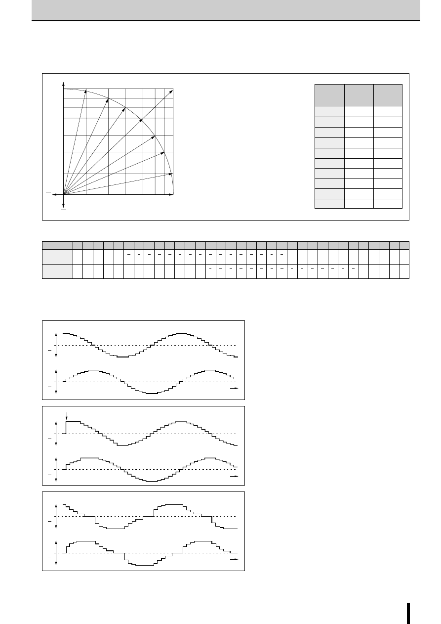
47
SLA7042M/SLA7044M
2-Phase Stepper Motor Unipolar Driver ICs (2W1-2 Phase Excitation/Micro-step Support)
SLA7042M/SLA7044M
■
Current Vector Locus (One step of stepper motor normalized to 90 degrees)
20
40
55.5
71.4 83 91
A
0
B
100
20
100
1
2
3
4
5
6
7
8
9
B
A
10
To rotate the motor, enter serial data as follows:
2W1-2 phase excitation
W1-2 phase excitation
1-2 phase excitation
2-2 phase excitation
: Vector 1
→
2
→
3
→
4
→
5
→
6
→
7
→
8
→
9 ...
: Vector 1
→
3
→
5
→
7
→
9
→
....
: Vector 1
→
5
→
9
: Vector 5 or 10
Combined
Current A Current B
vector
1
100%
0%
2
100%
20%
3
91%
40%
4
83%
55.5%
5
71.4%
71.4%
6
55.5%
83%
7
40%
91%
8
20%
100%
9
0%
100%
10
100%
100%
Sequence
DATA-A
MODE
DATA-B
MODE
20
0
7
27
7
1
■
Serial Data Sequence Example (2W 1-2 Phase Excitation for CW)
A malfunction may occur just after the power (V
DD
) is turned on because the internal logic is unstable. Therefore, set
the RESET state (REF terminal voltage: V
DD
−
1V to V
DD
) after the power is turned on.)
■
Operation Current Waveform Examples
Torque-up waveform at start
Stationary waveform
Leading phase waveform at acceleration
A
0
A
B
0
B
A
0
A
B
0
B
A
0
A
B
0
B
Start
Time
Time
Time
0
4
4
0
4
4
1
3
5
2
2
6
3
1
7
4
0
7
5
1
7
6
2
6
7
3
5
8
4
4
9
5
3
10
6
2
11
7
1
12
7
0
13
7
1
14
6
2
15
5
3
16
4
4
17
3
5
18
2
6
19
1
7
21
1
7
22
2
6
23
3
5
24
4
4
25
5
3
26
6
2
28
7
0
29
7
1
30
6
2
31
5
3
These three types of waveforms can all be set with a serial signal.
ac/Allegro/Allegro_Motor_Drive_ICs-html.html
48
PG001M
Serial Signal Generator IC for SLA7042M and SLA7044M
PG001M
CLOCK_IN
CLOCK_OUT
DATA
STROBE
T
CC
T
CS
1/F
1/F
CLOCK_OUT
DATA
STROBE
90%
10%
Tr
Tf
CLOCK_IN
RESET
MO
MS1
MS2
CW/CCW
VC
A
B
C
D
C
D
C
D
C
D
Excitation switching point
VC switching occurs only while CLOCK-IN level is L.
Fig. 1
Fig. 3 Timing conditions
Fig.2
(T
a
=25
°
C)
Parameter
Symbol
Conditions
Ratings
Units
min
typ
max
Supply voltage
V
DD
4.5
5.5
V
Supply current
I
DD
V
DD
=5.5V
0.35
0.45
mA
Output voltage
V
OH
V
DD
=5V, I
O
=
±
3mA
4.5
V
V
OL
0.4
Input current
I
I
V
DD
=5V, V
I
=0 or 5V
±
1
µ
A
Input voltage
V
IH
V
DD
=5V
3.5
5
V
V
IL
−
0.3
1.5
Input hysteresis voltage
V
H
V
DD
=5V
1
V
Input capacity
C
I
V
DD
=5V
5
10
pF
Internal oscillation frequency
F
V
DD
=5V
1.5
MHz
Propagation delay time
T
CS
See Fig. 1.
50
100
ns
T
CC
430
550
Output voltage
T
r
V
DD
=5V, C
L
=15pF
20
ns
Rise and fall time
T
f
See Fig. 2.
20
CLOCK IN terminal
V
CIH
H level time, V
DD
=5V
4.5
µ
s
Input clock time
V
CIL
L level time, V
DD
=5V
0.5
Reset setting time (A)
ts
R
Inter-clock
100
ns
Stabilization time after reset (B)
tps
R
See Fig. 3.
Signal setting time (C)
ts
S
Inter-clock
Stabilization time after
tps
S
See Fig. 3.
100
ns
signal input (D)
Parameter
Symbol
Ratings
Units
Supply voltage
V
DD
−
0.5 to 7
V
Input voltage
V
I
−
0.5 to V
DD
+0.5
V
Input current
I
I
±
10
mA
Output voltage
V
O
−
0.5 to V
DD
+0.5
V
Output current
I
O
±
15
mA
Power dissipation
P
D
200
mW
Operating temperature
T
OP
−
20 to +85
°
C
Storage temperature
T
stg
−
40 to +150
°
C
■
Absolute Maximum Ratings
(T
a
=25
°
C)
■
Electrical Characteristics
DC characteristics
AC characteristics
ac/Allegro/Allegro_Motor_Drive_ICs-html.html
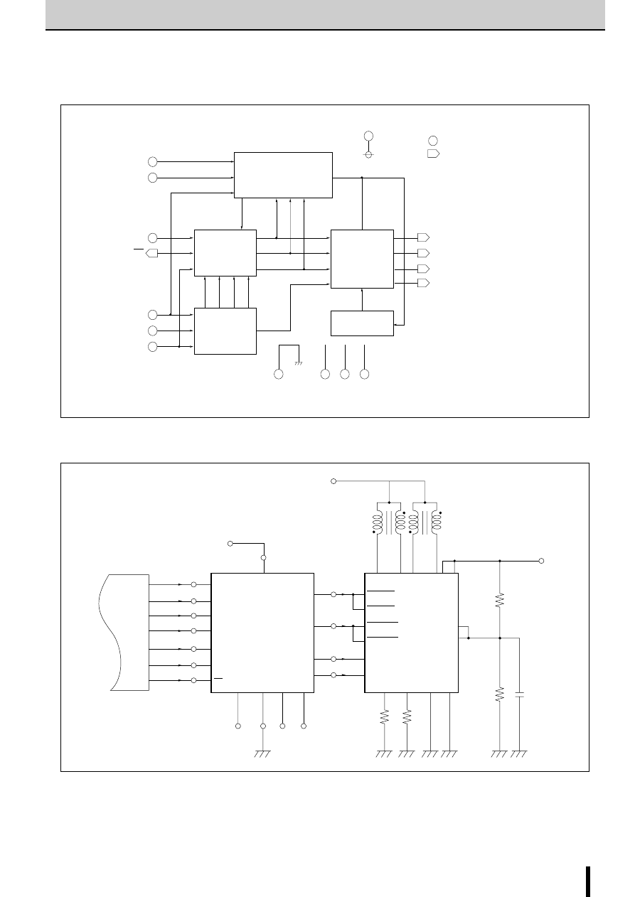
49
PG001M
PG001M
Serial Signal Generator IC for SLA7042M and SLA7044M
■
Internal Block Diagram
(A)
Excitation mode setting section
MS1
6
MS1
7
VC
2h
a
b
c
Q1 Q2
Q3 Q4
Phase
15
GND
8
VDD
SET
16
CLOCK_OUT
14
DATA_A
11
DATA_B
10
STROBE
13
CP1
5
CP2
4
NC
12
MO
9
CLOCK_IN
2
RESET
1
CW/CCW
3
(B)
Parallel signal
generator
(C)
Parallel-serial
signal converter
(D)
Up/Down counter
(E)
Oscillator
... Input
... Output
Number inside shape indicates pin number.
Fix all open input pins to H or L (Apart from CP1, CP2 and NC pins)
■
Diagram of Standard External Circuit
5V
16
MPU
VDD
RESET
CLOCK_IN
CLOCK
_OUT
CLOCK_A
CLOCK_B
STROBE_A
SLA7042M
SLA7044M
STROBE_B
DATA_A
DATA_B
STROBE
DATA_A
DATA_B
CW/CCW
MS1
MS2
VC
MO
NC
GND
CP1
CP2
1
14
13
11
10
2
3
6
7
15
12
NC
NC
NC
Rs
Rs
8
5
4
9
P
G
0
0
1
M
ac/Allegro/Allegro_Motor_Drive_ICs-html.html
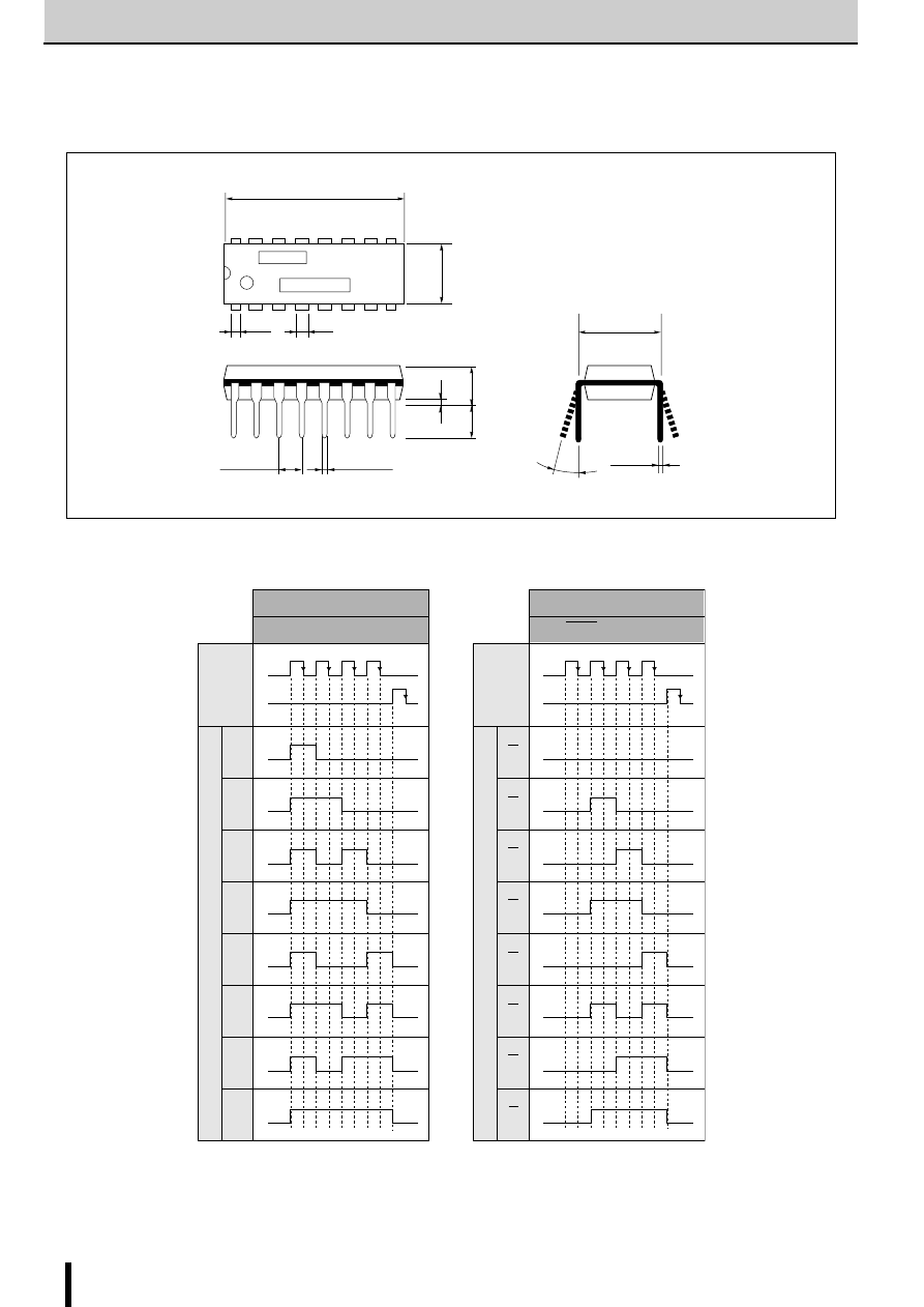
50
PG001M
PG001M
Serial Signal Generator IC for SLA7042M and SLA7044M
■
Output Mode Vs Output Pulse
Output pulse
OUT excitation
Output pulse
OUT excitation
CLOCK
_OUT
STROBE
0
0
0
0
0
0
0
0
0
0
0
0
0
0
0
0
0
0
0
Phase
a
0
1
2
3
4
5
6
7
0
1
2
3
4
5
6
7
b
c
Phase
a
b
c
CLOCK
_OUT
STROBE
Output mode
Output mode
■
External Dimensions
19.2
20.0max
6.3
6.65max
16
9
1
0.89
Lot No.
Part No.
2.54
±
0.25
0.48
±
0.10
0.51min
2.54min
5.08max
1.3
8
7.62
0.25
+0.11
−
0.05
0 to 15
°
C
(Unit: mm)
ac/Allegro/Allegro_Motor_Drive_ICs-html.html
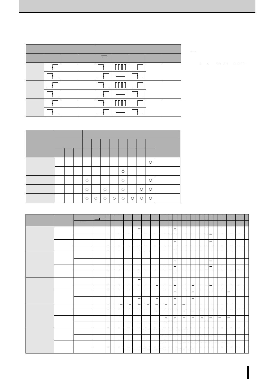
51
PG001M
PG001M
Serial Signal Generator IC for SLA7042M and SLA7044M
■
Input and Output Function Correlation Table
Input
Output
Mode
RESET
MO
STROBE
CLOCK
_IN
CW
/CCW
CLOCK
_OUT
DATA
-A
CW
CCW
CW
L
H
L
H
H
H
H
H
×
×
L
L
CCW
RESET
CW
CCW
DATA
-B
Output Mode
4 or 7
Output
Mode
Input Mode
4 or 7
Output
Mode
×
: Don't care
∗
: MO outputs L level while CLOCK_IN
is H level when output mode is 4:4
(7:7), 4:4 (7:7), 4:4 (7:7),or 4:4 (7:7).
Modes in brackets ( ) are for 2-2
phase VC: H.
■
Excitation Selection Table
■
Output Mode Sequence
Excitation method
Input
0
VC
H
L
L
L
H
L
L
L
−
−
−
−
−
−
−
−
−
−
−
−
−
−
−
−
−
−
−
−
−
−
L
H
×
×
H
H
×
MS1 MS2
0% 20% 40% 55.5% 71.4% 83% 91% 100%
141%
100%
100%
100%
100%
1
2
3
4
5
6
7
Output current mode of SLA7042M/7044M
Excitation mode
selection
Torque vector
2-2 Phase
Full Step
1-2 Phase
Half Step
W1-2 Phase
1/4 Step
2W1-2 Phase
1/8 Step
Excitation
method
2-2 Phase
Full Step (1)
(VC: H)
2-2 Phase
Full Step (2)
(VC: L)
1-2 Phase
Half Step
W1-2 Phase
1/4 Step
2W1-2 Phase
1/8 Step
1
H
=
=
=
=
=
=
=
=
=
=
=
=
=
=
=
=
3
5
5
3
CLOCK
MO
DATA_A
DATA_B
DATA_A
DATA_B
DATA_A
DATA_B
DATA_A
DATA_B
DATA_A
DATA_B
DATA_A
DATA_B
DATA_A
DATA_B
DATA_A
DATA_B
DATA_A
DATA_B
DATA_A
DATA_B
CW/CCW
CW
CCW
CW
CCW
CW
CCW
CW
CCW
CW
CCW
L
7
7
7
7
4
4
4
4
4
4
4
4
4
4
4
4
4
4
4
4
2
H
=
=
=
=
=
=
=
=
=
=
=
=
2
6
6
2
2
6
6
2
3
H
=
=
=
=
=
=
=
=
=
=
=
=
=
=
=
=
1
7
7
1
4
H
=
=
=
=
=
=
=
=
0
7
7
0
0
7
7
0
0
7
7
0
5
H
=
=
=
=
=
=
=
=
=
=
=
=
=
=
=
=
1
7
7
1
6
H
=
=
=
=
=
=
=
=
=
=
=
=
2
6
6
2
2
6
6
2
7
H
=
=
=
=
=
=
=
=
=
=
=
=
=
=
=
=
3
5
5
3
8
L
7
7
7
7
4
4
4
4
4
4
4
4
4
4
4
4
4
4
4
4
9
H
=
=
=
=
=
=
=
=
=
=
=
=
=
=
=
=
5
3
3
5
10
H
=
=
=
=
=
=
=
=
=
=
=
=
6
2
2
6
6
2
2
6
11
H
=
=
=
=
=
=
=
=
=
=
=
=
=
=
=
=
7
1
1
7
12
H
=
=
=
=
=
=
=
=
7
0
0
7
7
0
0
7
7
0
0
7
13
H
=
=
=
=
=
=
=
=
=
=
=
=
=
=
=
=
7
1
1
7
14
H
=
=
=
=
=
=
=
=
=
=
=
=
6
2
2
6
6
2
2
6
15
H
=
=
=
=
=
=
=
=
=
=
=
=
=
=
=
=
5
3
3
5
16
L
7
7
7
7
4
4
4
4
4
4
4
4
4
4
4
4
4
4
4
4
17
H
=
=
=
=
=
=
=
=
=
=
=
=
=
=
=
=
3
5
5
3
18
H
=
=
=
=
=
=
=
=
=
=
=
=
2
6
6
2
2
6
6
2
19
H
=
=
=
=
=
=
=
=
=
=
=
=
=
=
=
=
1
7
7
1
20
H
=
=
=
=
=
=
=
=
0
7
7
0
0
7
7
0
0
7
7
0
21
H
=
=
=
=
=
=
=
=
=
=
=
=
=
=
=
=
1
7
7
1
22
H
=
=
=
=
=
=
=
=
=
=
=
=
2
6
6
2
2
6
6
2
23
H
=
=
=
=
=
=
=
=
=
=
=
=
=
=
=
=
3
5
5
3
24
L
7
7
7
7
4
4
4
4
4
4
4
4
4
4
4
4
4
4
4
4
25
H
=
=
=
=
=
=
=
=
=
=
=
=
=
=
=
=
5
3
3
5
26
H
=
=
=
=
=
=
=
=
=
=
=
=
6
2
2
6
6
2
2
6
27
H
=
=
=
=
=
=
=
=
=
=
=
=
=
=
=
=
7
1
1
7
28
H
=
=
=
=
=
=
=
=
7
0
0
7
7
0
0
7
7
0
0
7
29
H
=
=
=
=
=
=
=
=
=
=
=
=
=
=
=
=
7
1
1
7
30
H
=
=
=
=
=
=
=
=
=
=
=
=
6
2
2
6
6
2
2
6
31
H
=
=
=
=
=
=
=
=
=
=
=
=
=
=
=
=
5
3
3
5
32
L
7
7
7
7
4
4
4
4
4
4
4
4
4
4
4
4
4
4
4
4
RESET
= : No output
ac/Allegro/Allegro_Motor_Drive_ICs-html.html
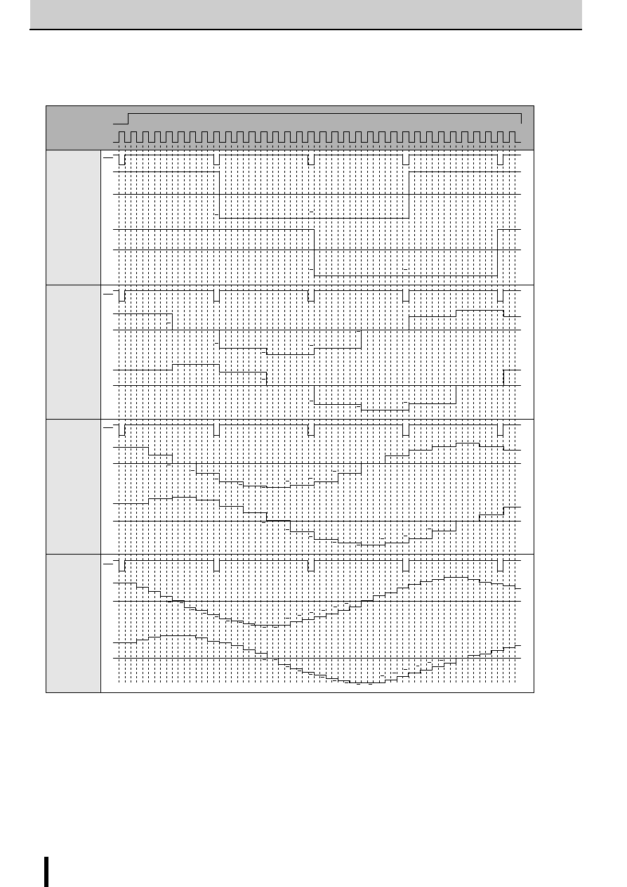
52
PG001M
PG001M
Serial Signal Generator IC for SLA7042M and SLA7044M
■
Output Timing Chart (CW)
…
Excitation Current of SLA7042M/7044M
RESET
CLOCK_IN
2-2 Phase
Full Step
(VC: H)
1-2 Phase
Half Step
W1-2 Phase
1/4 Step
2W1-2 Phase
1/8 Step
B
A
B
A
B
A
B
A
For 2-2 phase VC : L, output mode is 7
→
4.
7
7
7
0
7
2
0
2
4
4
2
6
0
3
5
6
2
7
1
7
0
7
1
6
2
5
3
4
4
3
5
2
6
1
7
0
7
1
7
6
5
4
3
2
1
0
1
2
3
4
5
6
7
7
7
6
5
4
3
5
4
3
2
1
0
1
2
3
4
5
6
7
7
7
6
5
4
3
2
7
2
6
4
4
6
2
7
0
6
2
4
4
2
6
0
7
2
6
4
4
6
7
6
4
4
0
4
4
0
7
4
4
7
0
4
4
7
7
7
7
7
7
7
7
MO
4
4
MO
4
4
MO
4
4
MO
ac/Allegro/Allegro_Motor_Drive_ICs-html.html
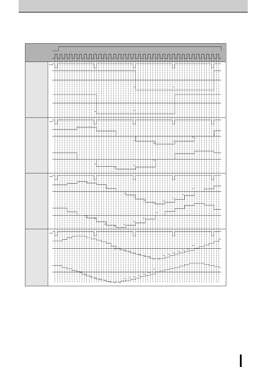
53
PG001M
PG001M
Serial Signal Generator IC for SLA7042M and SLA7044M
■
Output Timing Chart (CCW)
…
Excitation Current of SLA7042M/7044M
RESET
CLOCK_IN
2-2 Phase
Full Step
(VC: H)
1-2 Phase
Half Step
W1-2 Phase
1/4 Step
2W1-2 Phase
1/8 Step
For 2-2 phase VC:L, output mode is 7
→
4.
7
7
MO
4
4
MO
4
4
MO
4
4
MO
B
A
B
A
B
A
B
A
7
0
7
2
0
2
4
4
2
6
0
3
5
6
2
7
1
7
0
7
1
6
2
5
3
4
4
3
5
2
6
1
7
0
7
1
7
6
5
4
3
2
1
0
1
2
3
4
5
6
7
7
7
6
5
4
3
1
0
1
2
3
4
5
2
3
4
5
6
7
7
7
6
5
4
3
2
7
2
6
4
4
6
2
0
7
6
2
4
4
2
0
6
7
2
6
4
4
6
7
6
4
4
0
4
4
0
7
4
0
4
7
4
4
7
7
7
7
7
7
7
7
ac/Allegro/Allegro_Motor_Drive_ICs-html.html
54
A3966SA/SLB
2-Phase Stepper Motor Bipolar Driver IC
A3966SA/SLB
Allegro MicroSystems product
■
Features
●
Maximum output ratings: 30V,
±
650mA
●
Internal fixed-frequency PWM current con-
trol
●
Internal ground-clamp & flyback diodes
●
Internal thermal shutdown, crossover-cur-
rent protection and UVLO protection cir-
cuitry
●
Employs copper batwing lead frame with
low thermal resistance
■
Electrical Characteristics
Parameter
Symbol
Conditions
Ratings
Units
min
typ
max
Power outputs (OUT
A
or OUT
B
)
Load supply voltage range
V
BB
Operating, I
O
=
±
650mA, L=3mH
V
CC
30
V
Output leakage current
I
CEX
V
O
=30V
< 1.0
50
µ
A
V
O
=0V
<
−
1.0
−
50
µ
A
Source Driver, I
O
=
−
400mA
1.7
2.0
V
Output saturation voltage
V
CE
(sat)
Source Driver, I
O
=
−
650mA
1.8
2.1
V
Sink Driver, I
O
=+400mA, V
SENSE
=0.5V
0.3
0.5
V
Sink Driver, I
O
=+650mA, V
SENSE
=0.5V
0.4
1.3
V
Sense-current offset
I
SO
I
S
−
I
O
, I
O
=50~650mA
12
18
24
mA
Clamp diode forward voltage
V
F
I
F
=400mA
1.1
1.4
V
I
F
=650mA
1.4
1.6
V
Motor supply current (No load)
I
BB
(ON)
V
ENABLE1
=V
ENABLE2
=0.8V
3.0
5.0
mA
I
BB
(OFF)
V
ENABLE1
=V
ENABLE2
=2.4V
< 1.0
200
µ
A
Control logic
Logic supply voltage range
V
CC
Operating
4.75
5.50
V
Logic input voltage
V
IH
2.4
V
V
IL
0.8
V
Logic input current
I
IH
V
IN
=2.4V
< 1.0
20
µ
A
I
IL
V
IN
=0.8V
<
−
20
−
200
µ
A
Reference input voltage range
V
REF
Operating
0.1
2.0
V
Reference input current
I
REF
−
2.5
0
1.0
µ
A
Reference divider ratio
V
REF
/V
TRIP
3.8
4.0
4.2
Current-sense comparator input offset voltage
V
IO
V
REF
=0V
−
6.0
0
6.0
mV
Current-sense comparator input voltage range
V
S
Operating
−
0.3
1.0
V
PWM RC frequency
f
OSC
C
T
=680pF, R
T
=56k
Ω
22.9
25.4
27.9
kHz
PWM propagation delay time
t
PWM
Comparator Trip to Source OFF
1.0
1.4
µ
S
Cycle Reset to Source ON
0.8
1.2
µ
S
Cross-over dead time
t
codt
1k
Ω
Load to 25V
0.2
1.8
3.0
µ
S
I
O
=
±
650mA, 50% to 90% : ENABLE ON to Source ON
100
ns
I
O
=
±
650mA, 50% to 90% : ENABLE OFF to Source OFF
500
ns
I
O
=
±
650mA, 50% to 90% : ENABLE ON to Sink ON
200
ns
Propagation delay time
t
pd
I
O
=
±
650mA, 50% to 90% : ENABLE OFF to Sink OFF
200
ns
I
O
=
±
650mA, 50% to 90% : PHASE Change to Sink ON
2200
ns
I
O
=
±
650mA, 50% to 90% : PHASE Change to Sink OFF
200
ns
I
O
=
±
650mA, 50% to 90% : PHASE Change to Source ON
2200
ns
I
O
=
±
650mA, 50% to 90% : PHASE Change to Source OFF
200
ns
Thermal shutdown temperature
T
j
165
°
C
Thermal shutdown hysteresis
∆
T
j
15
°
C
UVLO enable threshold
V
UVLO en
Increasing V
CC
4.1
4.6
V
UVLO hysteresis
V
UVLO hys
0.1
0.6
V
Logic supply current
I
CC
(ON)
V
ENABLE1
=V
ENABLE2
=0.8V
50
mA
I
CC
(OFF)
V
ENABLE1
=V
ENABLE2
=2.4V
9
mA
●
"typ" values are for reference.
■
Absolute Maximum Ratings
Parameter
Symbol
Ratings
Units
A3966SA
A3966SLB
Load supply voltage
V
BB
30
V
Output current (peak)
I
O
(Peak)
±
750
mA
Output current (continuous)
I
O
±
650
mA
Logic supply voltage
V
CC
7.0
V
Logic input voltage range
V
IN
−
0.3 to V
CC
+0.3
V
Sense voltage
V
S
1.0
V
Package power dissipation
P
D
(Note1)
2.08
1.86
W
Ambient operating temperature
T
a
−
20 to +85
°
C
Junction temperature
T
j
(Note2)
+150
°
C
Storage temperature
T
stg
−
55 to +150
°
C
●
Output current rating may be limited by duty cycle, ambient temperature, and heat sinking. Under any
set of conditions, do not exceed the specified current rating or a junction temperature of 150
°
C.
Note 1: When ambient temperature is 25
°
C or over, derate using
−
16.67mW/
°
C (SA),
−
14.93mW/
°
C (SLB).
Note 2: Fault conditions where junction temperature (T
j
) exceeds 150
°
C will activate the device's thermal
shutdown circuitry. These conditions can be tolerated but should be avoided.
(Unless specified otherwise, T
a
=25
°
C, V
BB
=30V, V
CC
=4.75V to 5.5V, V
REF
=2V, V
S
= 0V, 56k
Ω
& 680pF RC to ground)
2-Phase/1-2 Phase Excitation
ac/Allegro/Allegro_Motor_Drive_ICs-html.html
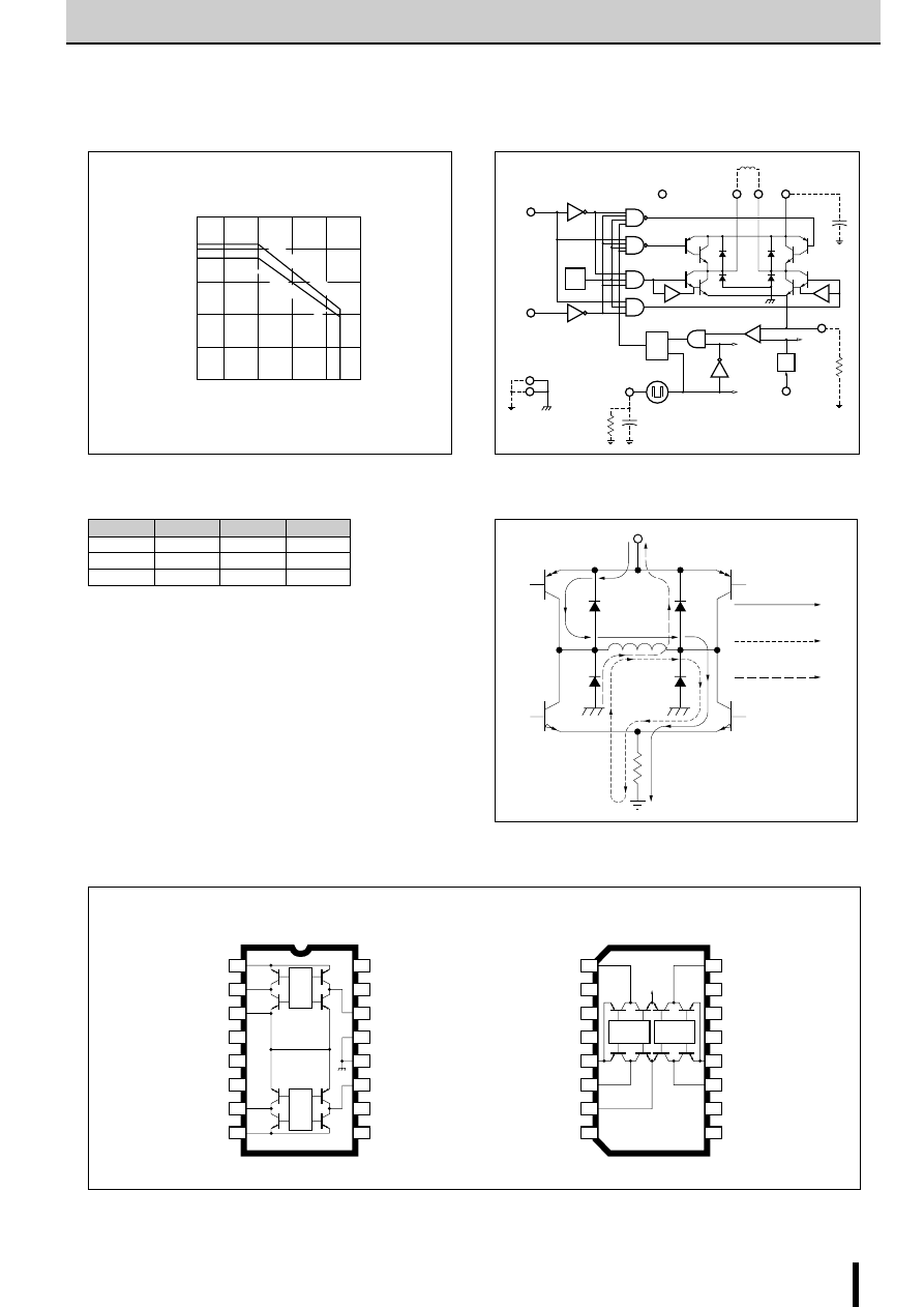
55
A3966SA/SLB
2-Phase Stepper Motor Bipolar Driver IC (2-Phase/1-2 Phase Excitation)
A3966SA/SLB
■
Derating
Allowable package power dissipation P
D
[W]
0
0.5
1
1.5
2
2.5
Ambient temperature Ta (
°
C)
−
20
0
25
50
75 85 100
A3966SLB 67
°
C/W
A3966SA 60
°
C/W
■
Internal Block Diagram (1/2 circuit)
PHASE
ENABLE
(ACTIVE LOW)
GROUND
OSC
RC
Q
R
+4
+
−
+
S
TO OTHER
BRIDGE
TO OTHER
BRIDGE
TO OTHER
BRIDGE
BLANKING
GATE
PWM LATCH
CURRENT-SENSE
COMPARATOR
SENSE
R
T
C
T
R
S
UVLO
& TSD
LOGIC
SUPPL
Y
LO
AD
SUPPL
Y
OUT
A
OUT
B
REFERENCE
V
CC
V
BB
■
Truth Table
■
Load-Current Paths
PHASE
ENABLE
OUT
A
OUT
B
X
H
Z
Z
H
L
H
L
L
L
L
H
X: Don't care (either L or H)
Z: High impedance (source and sink both OFF)
V
BB
R
S
BRIDGE ON
SOURCE OFF
ALL OFF
■
Terminal Connection Diagram
1
2
3
4
LOGIC
LOGIC
5
6
7
8
16
15
14
13
12
11
10
9
OUT
1A
PHASE
1
ENABLE
1
GROUND
SENSE
1
OUT
1B
LOAD
SUPPLY
REFERENCE
OUT
2A
PHASE
2
ENABLE
2
GROUND
SENSE
2
OUT
2B
V
BB
V
BB
V
CC
V
REF
LOGIC
SUPPLY
RC
RC
1
2
3
4
LOGIC
LOGIC
5
6
7
8
16
15
14
13
12
11
10
9
OUT
1A
PHASE
1
ENABLE
1
SENSE
1
OUT
1B
LOAD
SUPPLY
REFERENCE
OUT
2A
PHASE
2
ENABLE
2
GROUND
GROUND
SENSE
2
OUT
2B
V
BB
V
CC
V
REF
LOGIC
SUPPLY
RC
RC
A3966SA
A3966SLB
ac/Allegro/Allegro_Motor_Drive_ICs-html.html
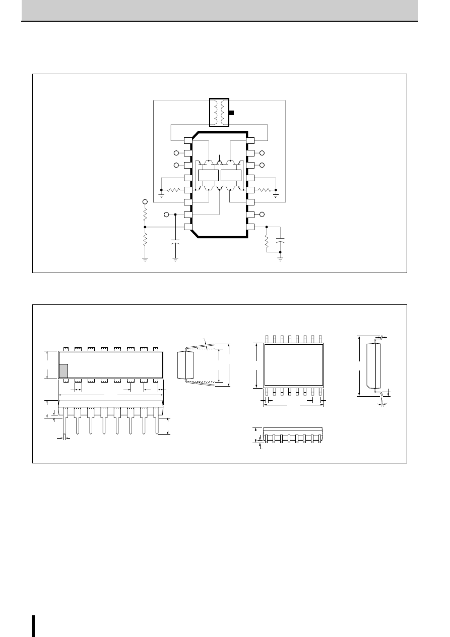
56
A3966SA/SLB
2-Phase Stepper Motor Bipolar Driver IC (2-Phase/1-2 Phase Excitation)
A3966SA/SLB
■
External Dimensions
(Unit: mm)
7.11
6.10
5.33
MAX
3.81
2.93
1.77
1.15
0.13
MIN
0.355
0.204
0.39
MIN
0.558
0.356
16
1
8
2.54
BSC
9
19.68
18.67
7.62
BSC
10.92
MAX
0.32
0.23
1.27
0.40
1.27
BSC
0
°
to 8
°
10.65
10.00
7.60
7.40
2.65
2.35
0.51
0.33
1
16
9
2
3
0.10 MIN.
10.50
10.10
A3966SA
A3966SLB
■
Typical Application
I
TRIP
≅
I
OUT
+I
SO
≅
V
REF
/(4
•
R
S
)
t
blank
≅
1,900
•
C
T
f
OSC
≅
1/ (R
T
•
C
T
+t
blank
)
R
T
=56k
Ω
(20k
Ω
to 100k
Ω
)
C
T
=680pF(470pF to 1,000pF)
Example of stepper motor drive
3
5
6
7
8
15
14
13
12
11
10
9
LOGIC
LOGIC
V
BB
V
BB
V
CC
V
REF
RC
1
16
PHASE
A
PHASE
B
ENABLE
B
+5 V
ENABLE
A
39 k
Ω
56 k
Ω
680 pF
0.5
Ω
10 k
Ω
+5V
+24 V
0.5
Ω
2
4
+
47 F
µ
(A3966SLB)
ac/Allegro/Allegro_Motor_Drive_ICs-html.html

57
A3966SA/SLB
ac/Allegro/Allegro_Motor_Drive_ICs-html.html
58
A3964SLB
2-Phase Stepper Motor Bipolar Driver IC
A3964SLB
Allegro MicroSystems product
■
Features
●
Fixed off-time PWM current control
●
Internally generated, precision 2.5V refer-
ence
●
External filter for sense terminal not required
●
Internal thermal shutdown circuitry
●
Internal crossover-current protection cir-
cuitry
●
Internal UVLO protection
●
Internal transient-suppression diodes
●
Low thermal resistance 20-pin SOP
■
Absolute Maximum Ratings
Parameter
Symbol
Ratings
Units
Load supply voltage
V
BB
30
V
Output current (continuous)
I
O
±
0.80
A
Logic supply voltage
V
CC
7.0
V
Logic input voltage range
V
IN
−
0.3 to V
CC
+0.3
V
Continuous output emitter voltage
V
E
1.0
V
Reference output current
I
REF-OUT
1.0
mA
Package power dissipation
P
D
(Note1)
2.08
W
Operating temperature
T
a
−
20 to +85
°
C
Junction temperature
T
j
(Note2)
+150
°
C
Storage temperature
T
stg
−
55 to +150
°
C
●
Output current rating may be limited by duty cycle, ambient temperature, and heat sinking. Under any
set of conditions, do not exceed the specified current rating or a junction temperature of 150
°
C.
Note 1: When ambient temperature is 25
°
C or over, derate using
−
16.7mW/
°
C.
Note 2: Fault conditions where junction temperature (T
j
) exceeds 150
°
C will activate the device's thermal
shutdown circuitry. These conditions can be tolerated but should be avoided.
Parameter
Symbol
Conditions
Ratings
Units
min
typ
max
Power outputs (OUT
A
or OUT
B
)
Load supply voltage range
V
BB
Operating
5
30
V
Output leakage current
I
CEX
Sink driver, V
O
=V
BB
< 1.0
50
µ
A
Source driver, V
O
=0V
<
−
1.0
−
50
µ
A
Sink driver, I
O
=+500mA
0.3
0.6
V
Sink driver, I
O
=+750mA
0.5
1.2
V
Output saturation voltage
V
CE (SAT)
Sink driver, I
O
=+800mA
1.5
V
Source driver, I
O
=
−
500mA
1.0
1.2
V
Source driver, I
O
=
−
750mA
1.1
1.5
V
Source driver, I
O
=
−
800mA
1.7
V
Output sustaining voltage
V
CE (SUS)
I
O
=
±
800mA, L=3mH
30
V
Clamp diode leakage current
I
R
V
R
=30V
< 1.0
50
µ
A
Clamp diode forward voltage
V
F
I
F
=800mA
1.6
2.0
V
Motor supply current
I
BB (ON)
V
EN1
=V
EN2
=0.8V, no load
10
mA
I
BB (OFF)
V
EN1
=V
EN2
=2.4V, no load
10
mA
Control logic
Logic input voltage
V
IH
2.4
V
V
IL
0.8
V
Logic input current
I
IH
V
IN
=2.4V
<
−
1.0
20
µ
A
I
IL
V
IN
=0.8V
<
−
20
−
200
µ
A
Reference output voltage
V
REF
•
OUT1
V
CC
=5.0V, I
REF
•
OUT
=90~900
µ
A
2.45
2.50
2.55
V
Current-sense comparator input current
I
REF
•
IN
V
REF
•
IN
=1V
−
5.0
5.0
µ
A
Current-sense comparator input voltage range
V
REF
•
IN
Operating
−
0.3
1.0
V
Current-sense comparator input offset voltage
V
TH
V
REF
•
IN
=0V
−
6
6
mV
Timer blanking charge current (RC off)
I
RC
V
RC
=2.0V
1.0
mA
Timer blanking threshold (RC off)
V
BLTH(1)
3.0
V
V
BLTH(0)
1.0
V
Timer blanking OFF voltage (RC off)
V
RCOFF
R
T
=20k
Ω
3.0
V
Thermal shutdown temperature
T
j
165
°
C
Thermal shutdown hysteresis
∆
T
j
15
°
C
Logic supply current
I
CC (ON)
V
EN1
=V
EN2
=0.8V, no load
65
85
mA
I
CC (OFF)
V
EN1
=V
EN2
=2.4V, no load
17
mA
Logic supply current/temperature coefficient
∆
I
CC (ON)
V
EN1
=V
EN2
=0.8V, no load
0.18
mA/
°
C
●
"typ" values are for reference.
Note) Logic input: En1, En2, Ph1, Ph2
(Unless specified otherwise, V
IN
=V
DD
or GND)
OUT
1B
OUT
1A
GROUND
GROUND
V
BB
RC
1
PHASE
1
ENABLE
1
V
REF
IN
SENSE
1
OUT
2B
OUT
2A
GROUND
GROUND
V
CC
RC
2
PHASE
2
ENABLE
2
V
REF
OUT
SENSE
2
1
2
3
4
5
6
7
8
9
10
11
12
13
14
15
16
17
18
19
20
2.5
1.5
1.0
0.5
2.0
0
−
20
0
25
50
75
100
85
60
°
C/
W
Ambient temperature Ta (
°
C)
Allo
w
a
b
le pac
kage po
w
e
r dissipation P
D (
W)
■
Terminal Connection Diagram
■
Derating
2-Phase/1-2 Phase Excitation
■
Electrical Characteristics
(Unless specified otherwise, T
a
=25
°
C, V
BB
=30V, V
CC
=4.75V to 5.25V, V
REF
=2V, V
SENSE
= 0V)
ac/Allegro/Allegro_Motor_Drive_ICs-html.html
59
A3964SLB
2-Phase Stepper Motor Bipolar Driver IC (2-Phase/1-2 Phase Excitation)
A3964SLB
■
External Dimensions
Wide body plastic SOP (300mil)
■
Internal Block Diagram(Dotted Line)/
Diagram of Standard External Circuit (Recommended Circuit Constants)
■
Excitation Sequence
[1-2 phase excitation]
(Unit: mm)
[2-phase excitation]
■
Truth Table
ICs per stick
37
Phase
Phase 1
0
1
2
3
0
H
L
L
H
H
L
L
L
L
L
H
H
L
L
H
L
L
L
L
L
Enable 1
Enable 2
Phase 2
Phase 1
0
1
2
3
4
5
6
7
0
H
H
X
L
L
L
X
H
H
L
L
H
L
L
L
H
L
L
X
H
H
H
X
L
L
L
X
H
L
L
L
H
L
L
L
H
Enable 1
Enable 2
Phase 2
Enable
Out A
Out B
H
L
L
L
L
L
Z
Z
H
H
H
X
X = Don't care, Z = High impedance
+
−
+
−
Blanking time &
one shot multi
Blanking time &
one shot multi
RC
1
R
T1
R
S1
R
S2
C
T2
R
T2
R
1
=20k
Ω
R
2
=5k
Ω
(VR)
R
T
=30k
Ω
C
T
=1000pF
R
S
=0.68 to 1.5
Ω
(1 to 2W)
R
C2
V
CC
V
BB
V
BB
(5~30V)
V
CC
(5V)
Sen
1
V
REF
V
REF
Sen
2
R
1
R
2
C
T1
8
GND
OUT
IN
13
12
18
20
17
4
11
19
16
15
6
5
7
2
14
Phase 2
Enable 2
Source off
TSD
3
1
9
10
Phase 1
Enable 1
Source off
1.27
0.40
0.32
0.23
10.65
10.00
7.60
7.40
13.00
12.60
0.51
0.33
1
10
11
20
*1
2.65
2.35
SEATING PLANE
0.10 MIN
1.27
BSC
0
°
TO 8
°
OUT
2A
OUT
2B
OUT
1A
OUT
1B
Note) [Pin] material : copper
Surface treatment : solder plating
Note) Package index may be *1.
Reference voltage
power supply
+
ac/Allegro/Allegro_Motor_Drive_ICs-html.html
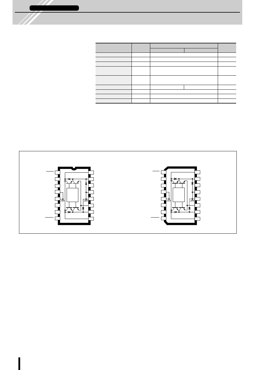
60
A3953SB/SLB
2-Phase Stepper Motor Bipolar Driver ICs
A3953SB/SLB
■
Terminal Connection Diagram
1
MODE
GROUND
GROUND
LOGIC
SUPPLY
PHASE
GROUND
GROUND
RC
SENSE
LOAD
SUPPLY
BRAKE
REF
LOAD
SUPPLY
OUT
B
OUT
A
V
BB
V
BB
V
CC
ENABLE
2
6
7
8
16
15
3
14
9
10
11
LOGIC
A3953SLB
A3953SB
1
MODE
GROUND
GROUND
LOGIC
SUPPLY
PHASE
GROUND
GROUND
RC
SENSE
LOAD
SUPPLY
BRAKE
REF
LOAD
SUPPLY
OUT
B
OUT
A
V
BB
V
BB
V
CC
ENABLE
2
6
7
8
16
15
3
14
9
10
11
4
5
12
13
4
5
12
13
■
Absolute Maximum Ratings
Parameter
Symbol
Ratings
Units
A3953SB
A3953SLB
Load supply voltage
V
BB
50
V
Output current (continuous)
I
O
±
1.3
A/unit
Logic supply voltage
V
CC
7.0
V
Logic/reference input
V
IN
−
0.3 to V
CC
+0.3
V
voltage range
Sense voltage
V
SENSE
D.C.
1.0 (V
CC
=5.0V)
V
0.4 (V
CC
=3.3V)
Package power dissipation P
D
(Note1)
2.90
1.86
W/pkg
Operating temperature
T
a
−
20 to +85
°
C
Junction temperature
T
j
(Note2)
+150
°
C
Storage temperature
T
stg
−
55 to +150
°
C
●
Output current rating may be limited by duty cycle, ambient temperature, and heat sinking. Under any
set of conditions, do not exceed the specified current rating or a junction temperature of 150
°
C.
Note 1: When ambient temperature is 25
°
C or over, derate using
−
23.26mW/
°
C(SB) or
−
14.93mW/
°
C(SLB).
Note 2: Fault conditions where junction temperature (T
j
) exceeds 150
°
C will activate the device’s thermal
shutdown circuitry. These conditions can be tolerated but should be avoided.
■
Features
●
Fixed off-time PWM current control
●
Switching between power supply regenera-
tion mode and loop regeneration mode in
order to improve motor current response in
microstepping
●
External filter for sense terminal not required
●
3.3V and 5V logic supply voltage
●
Sleep (low current consumption) mode
●
Brake operation with PWM current limiting
●
Internal thermal shutdown circuitry
●
Internal crossover-current protection cir-
cuitry
●
Internal UVLO protection
●
Internal transient-suppression diodes
●
Low thermal resistance package
Allegro MicroSystems product
2-Phase/1-2 Phase Excitation
ac/Allegro/Allegro_Motor_Drive_ICs-html.html
61
A3953SB/SLB
2-Phase Stepper Motor Bipolar Driver ICs (2-Phase/1-2 Phase Excitation)
A3953SB/SLB
■
Electrical Characteristics
Parameter
Symbol
Conditions
Limits
Units
min
typ
max
Power outputs (OUT
A
or OUT
B
)
Load supply voltage range
V
BB
Operating, I
O
=
±
1.3A, L=3mH
V
CC
50
V
Output leakage current
I
CEX
V
O
=V
BB
<1.0
50
µ
A
V
O
=0V
<
−
1.0
−
50
µ
A
Sense current offset
I
SO
I
SENSE
−
I
O
, I
O
=850mA, V
SENSE
=0V, V
CC
=5V
18
33
50
mA
V
SENSE
=0.4V, V
CC
=3.0V, BRAKE=H:Source driver, I
O
=
−
0.85A
1.0
1.1
V
Output saturation voltage
V
CE (SAT)
V
SENSE
=0.4V, V
CC
=3.0V, BRAKE=H:Source driver, I
O
=
−
1.3A
1.7
1.9
V
(Forward/reverse mode)
V
SENSE
=0.4V, V
CC
=3.0V, BRAKE=H:Sink driver, I
O
=0.85A
0.4
0.9
V
V
SENSE
=0.4V, V
CC
=3.0V, BRAKE=H:Sink driver, I
O
=1.3A
1.1
1.3
V
Output saturation voltage
V
CE (SAT)
V
SENSE
=0.4V, V
CC
=3.0V, BRAKE=L:Sink driver, I
O
=0.85A
1.2
1.4
V
(Brake mode)
V
SENSE
=0.4V, V
CC
=3.0V, BRAKE=L:Sink driver, I
O
=1.3A
1.4
1.8
V
Clamp diode forward voltage
V
F
I
F
=0.85A
1.2
1.4
V
I
F
=1.3A
1.4
1.8
V
I
BB (ON)
V
ENABLE
=0.8V, V
BRAKE
=2.0V
2.5
4.0
mA
Motor supply current
I
BB (OFF)
V
ENABLE
=V
BRAKE
=2.0V, V
MODE
=0.8V
1.0
50
µ
A
(No load)
I
BB (BRAKE)
V
BRAKE
=0.8V
1.0
50
µ
A
I
BB (SLEEP)
V
ENABLE
=V
BRAKE
=V
MODE
=2.0V
1.0
50
µ
A
Control logic
Thermal shutdown temperature
T
j
165
°
C
Thermal shutdown hysteresis
∆
T
j
8
°
C
UVLO enable threshold
V
UVLO
2.5
2.75
3.0
V
UVLO hysteresis
∆
V
UVLO
0.12
0.17
0.25
V
I
CC (ON)
V
ENABLE
=0.8V, V
BRAKE
=2.0V
42
50
mA
Logic supply current
I
CC (OFF)
V
ENABLE
=V
BRAKE
=2.0V, V
MODE
=0.8V
12
15
mA
I
CC (BRAKE)
V
BRAKE
=0.8V
42
50
mA
I
CC (SLEEP)
V
ENABLE
=V
BRAKE
=V
MODE
=2.0V
500
800
µ
A
Logic supply voltage range
V
CC
Operating
3.0
3.3
V
5.0
5.5
Logic input voltage
V
IH
2.0
V
V
IL
0.8
V
Logic input current
I
IH
V
IN
=2.0V
<1.0
20
µ
A
I
IL
V
IN
=0.8V
<
−
2.0
−
200
µ
A
Sense voltage range
V
SENSE (3.3)
V
CC
=3.0V to 3.6V
0
0.4
V
V
SENSE (5.0)
V
CC
=4.5V to 5.5V
0
1.0
V
Reference input current
I
REF
V
REF
=0V to 1V
±
5.0
µ
A
Comparator input offset voltage
V
IO
V
REF
=0V
±
2.0
±
5.0
mV
AC timing
PWM RC fixed off-time
t
OFF RC
C
T
=680pF, R
T
=30k
Ω
, V
CC
=3.3V
18.3
20.4
22.5
µ
s
PWM turn-off time
t
PWM (OFF)
Comparator Trip to Source OFF, Io=25mA
1.0
1.5
µ
s
Comparator Trip to Source OFF, Io=1.3A
1.8
2.6
µ
s
PWM turn-on time
t
PWM (ON)
I
RC
Charge ON to Source ON, Io=25mA
0.4
0.7
µ
s
I
RC
Charge ON to Source ON, Io=1.3A
0.55
0.85
µ
s
PWM minimum on-time
t
PWM (ON)
V
CC
=3.3V, R
T
≥
12k
Ω
, C
T
=680pF
0.8
1.4
1.9
µ
s
V
CC
=5.0V, R
T
≥
12k
Ω
, C
T
=470pF
0.8
1.6
2.0
µ
s
I
O
=
±
1.3A, 50% to 90% ENABLE ON to Source ON
1.0
µ
s
I
O
=
±
1.3A, 50% to 90% ENABLE OFF to Source OFF
1.0
µ
s
I
O
=
±
1.3A, 50% to 90% ENABLE ON to Sink ON
1.0
µ
s
Propagation delay time
t
pd
I
O
=
±
1.3A, 50% to 90% ENABLE OFF to Sink OFF (MODE=L)
0.8
µ
s
I
O
=
±
1.3A, 50% to 90% PHASE Change to Sink ON
2.4
µ
s
I
O
=
±
1.3A, 50% to 90% PHASE Change to Sink OFF
0.8
µ
s
I
O
=
±
1.3A, 50% to 90% PHASE Change to Source ON
2.0
µ
s
I
O
=
±
1.3A, 50% to 90% PHASE Change to Source OFF
1.7
µ
s
Crossover dead time
t
CODT
1k
Ω
Load to 25V, V
BB
=50V
0.3
1.5
3.0
µ
s
●
“typ” values are for reference.
(Unless specified otherwise, T
a
=25
°
C, V
BB
=5V to 50V, V
CC
=3.0V to 5.5V)
ac/Allegro/Allegro_Motor_Drive_ICs-html.html
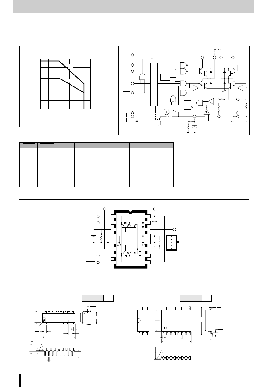
62
A3953SB/SLB
2-Phase Stepper Motor Bipolar Driver ICs (2-Phase/1-2 Phase Excitation)
A3953SB/SLB
■
Derating
■
Internal Block Diagram
■
Truth Table
■
External Dimensions
■
Application Circuit
(16-pin wide SOIC)
ENABLE
BRAKE
PHASE
MODE
Operating Mode
OUT
A
OUT
B
H
H
H
H
H
H
L
L
H
H
L
L
L
L
X
X
X
X
H
H
L
L
X
X
H
L
H
L
H
L
H
L
Z
Z
H
H
L
L
L
L
Z
Z
L
L
H
H
L
L
Sleep mode
Standby
Forward, fast current-decay mode
Forward, slow current-decay mode
Reverse, fast current-decay mode
Reverse, slow current-decay mode
Brake, fast current-decay mode
Brake, no current control
ICs per stick
47
X : Don't Care
Z : High impedance
V
BB
RC
V
CC
LOGIC
SUPPLY
LOAD
SUPPLY
PHASE
R
S
MODE
REF
OUT
A
OUT
B
ENABLE
SENSE
−
+
BRAKE
GROUND
PWM LATCH
V
CC
BLANKING
SLEEP &
STANDBY MODES
V
TH
R
T
C
T
6
GROUND
LOAD
SUPPLY
14
7
8
1
5
4
INPUT LOGIC
Q
R
S
3
2
+
−
11
12
13
10
15
16
9
UVLO
& TSD
2.0
3.0
2.5
1.5
1.0
0.5
0
−
20
0
25
50
75
100
85
A3953SB 43
C
°
/ W
A3953SLB 67
C
°
/ W
Ambient temperature Ta (C
°
)
Allowable package power dissipation P
D
(W)
1.27
0.40
0.32
0.23
10.65
10.00
7.60
7.40
10.50
10.10
0.51
0.33
1
8
9
16
*1
2.65
2.35
SEATING PLANE
0.10 MIN.
1.27
BSC
0
°
TO 8
°
●
●
●
●
Pin material: copper,
pin surface treatment: solder plating
Package index may be *1.
Allowable variation in distance between
leads is not cumulative.
Web (batwing) type lead frames are used for
pin 4, 5, 12, 13. The pins are connected to GND.
47 F
+
1
V
BB
V
BB
V
CC
V
BB
LOGIC
30 k
Ω
0.5
Ω
MODE
PHASE
ENABLE
BRAKE
680 pF
+5 V
REF
9
2
3
4
5
6
7
8
15
16
12
13
14
10
11
t
OFF
≅
R
T
•
C
T
R
T=
12k to 100k
Ω
C
T=
470 to 1500pF (Operating at V
CC=
5V)
C
T=
680 to 1500pF (Operating at V
CC=
3.3V)
Off-time setting
(DC motor drive)
(A3953SB)
Plastic DIP (300mil)
1.77
1
2
3
8
9
16
1.15
21.33
18.93
0.558
0.356
4.06
2.93
7.11
6.10
INDEX AREA
0.127MIN
7.62BSC
2.54BSC
5.33MAX
SEATING PLANE
0.39MIN
0.381
0.204
●
●
Note 1:
2:
Thickness of lead is measured
below seating plane.
Allowable variation in distance between
leads is not cumulative.
Lead width of pin 1, 8, 9, 16 may be
half the value shown here.
Maximum thickness of lead is 0.508mm.
ICs per stick
25
A3953SB
A3953SLB
(Unit: mm)
µ
ac/Allegro/Allegro_Motor_Drive_ICs-html.html
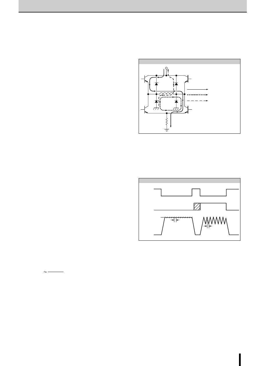
63
A3953SB/SLB
2-Phase Stepper Motor Bipolar Driver ICs (2-Phase/1-2 Phase Excitation)
A3953SB/SLB
■
Outline
Designed for bidirectional pulse-width modulated (PWM) cur-
rent control of inductive loads, the A3953S- is capable of con-
tinuous output currents to
±
1.3A and operating voltages to 50V.
Internal fixed off-time PWM current-control circuitry can be used
to regulate the mximum load current to a desired value. The
peak load current limit is set by the user’s selection of an input
reference voltage and external sensing resistor. The fixed off-
time pulse duration is set by a userselected external RC timing
network. Internal circuit protection includes thermal shutdown
with hysteresis, transient-suppression diodes, and crossover cur-
rent protection. Special power-up sequencing is not required.
With the ENABLE input held low, the PHASE input controls load
current polarity by selecting the appropriate source and sink
driver pair. The MODE input determines whether the PWM cur-
rent-control circuitry operates in a slow current-decay mode (only
the selected source driver switching) or in a fast current-decay
mode (selected source and sink switching). A user-selectable
blanking window prevents false triggering of the PWM current-
control circuitry. With the ENABLE input held high, all output
drivers are disabled. A sleep mode is provided to reduce power
consumption.
When a logic low is applied to the Brake input, the braking func-
tion is enabled. This overrides ENABLE and PHASE to turn OFF
both source drivers and turn ON both sink drivers. The brake
function can be used to dynamically brake brush dc motors.
■
FUNCTIONAL DESCRIPTION
(A) Internal PWM Current Control During Forward and Re-
verse Operation.
The A3953S-contains a fixed off-time pulse-width modulated
(PWM) current-control circuit that can be used to limit the load
current to a desired value. The peak value of the current limiting
(I
TRIP
) is set by the selection of an external current sensing re-
sistor (R
S
) and reference input voltage (V
REF
). The internal cir-
cuitry compares the voltage across the external sense resistor
to the voltage on the reference input terminal (REF) resulting in
a transconductance function approximated by:
where I
SO
is the offset due to base drive current.
In forward or reverse mode the current-control circuitry limits
the load current as follows: when the load current reaches I
TRIP
,
the comparator resets a latch that turns off the selected source
driver or selected sink and source driver pair depending on
whether the device is operating in slow or fast current-decay
mode, respectively.
In slow current-decay mode, the selected source driver is dis-
abled; the load inductance causes the current to recirculate
through the sink driver and ground clamp diode. In fast current-
I
TRIP
−
I
SO
R
SENSE
V
REF
R
S
V
BB
DRIVE CURRENT
RECIRCULATION (SLOW-DECAY MODE)
RECIRCULATION (FAST-DECAY MODE)
Fig. 1 Load-current Paths
ENABLE
MODE
LOAD
CURRENT
RC
I
TRIP
RC
Fig. 2 Fast and Slow Current-Decay Waveforms
Application Notes
decay mode, the selected sink and source driver pair are dis-
abled; the load inductance causes the current to flow from ground
to the load supply via the ground clamp and flyback diodes.
The user selects an external resistor (R
T
) and capacitor (C
T
) to
determine the time period (t
OFF
=R
T
•
C
T
) during which the drivers
remain disabled (see “RC Fixed Off-time” below). At the end of
the RC interval, the drivers are enabled allowing the load cur-
rent to increase again. The PWM cycle repeats, maintaing the
peak load current at the desired value (see figure 2).
(B)INTERNAL PWM CURRENT CONTROL DURING BRAKE-
MODE OPERATION
(1) Brake Operation-MODE Input High.
The brake circuit turns OFF both source drivers and turns ON
both sink drivers. For dc motor applications, this has the effect
of shoring the motor’s back-EMF voltage resulting in current
flow that dynamically brakes the motor. If the back-EMF volt-
age is large, and there is no PWM current limiting, the load cur-
rent can increase to a value that approaches that of a locked
rotor condition. To limit the current, when the I
TRIP
level is reaced,
the PWM circuit disables the conducting sink drivers. The en-
ergy stored in the motor’s inductance is discharged into the load
supply causing the motor current to decay.
As in the case of forward/reverse operation, the drivers are en-
abled after a time given by t
OFF
=R
T
•
C
T
(see “RC Fixed Off-time”
below). Depending on the back-EMF voltage (proportional to
the motor’s decreasing speed), the load current again may in-
ac/Allegro/Allegro_Motor_Drive_ICs-html.html

64
A3953SB/SLB
2-Phase Stepper Motor Bipolar Driver ICs (2-Phase/1-2 Phase Excitation)
A3953SB/SLB
1.05
•
(t
on (min)
max + t
off
)
•
R
LOAD
[(V
BB
−
V
SAT (source
+
sink)
)
•
t
on (min)
max]
−
[1.05
•
(V
SAT (sink)
+ V
F
)
•
t
off
]
I
AVE
≅
I
TRIP BRAKE MH
R
SENSE
V
REF
I
PEAK BRAKE ML
R
LOAD
V
BEMF
−
1V
t
off
R
T
•
C
T
crease to I
TRIP
. If so, the PWM cycle will repeat, limiting the peak
load current to the desired value.
During braking, when the MODE input is high, the peak current
limit can be approximated by:
CAUTION: Because the kinetic energy stored in the motor and
load inertia is being converted into current, which charges the
V
BB
supply bulk capacitance (power supply output and
decoupling capacitance), care must be taken to ensure the ca-
pacitance is sufficient to absorb the energy without exceeding
the voltage rating of any devices connected to the motor sup-
ply.
(2) Brake Operation-MODE Input Low.
During braking, with the MODE input low, the internal current-
control circuitry is disabled. Therefore, care should be taken to
ensure that the motor’s current does not exceed the ratings of
the device. The braking current can be measured by using an
oscilloscope with a current probe connected to one of the motor’s
leads, or if the back-EMF voltage of the motor is known, ap-
proximated by:
(C) RC Fixed Off-Time.
The internal PWM current-control circuitry uses a one shot to
control the time the driver (s) remain (s) off. The one-shot time,
t
OFF
(fixed off-time), is determined by the selection of an exter-
nal resistor (R
T
) and capacitor (C
T
) connected in parallel from
the RC timing terminal to ground. The fixed off-time, over a range
of values of C
T
=470pF to 1500pF and R
T
=12k
Ω
to 100k
Ω
, is
approximated by:
The operation of the circuit is as follows: when the PWM latch is
reset by the current comparator, the voltage on the RC terminal
will begin to decay from approximately 0.60V
CC
. When the volt-
age on the RC terminal reaches approximately 0.22 V
CC
, the
PWM latch is set, thereby enabling the driver (s).
(D) RC Blanking.
In addition to determining the fixed off-time of the PWM control
circuit, the C
T
component sets the comparator blanking time.
This function blanks the output of the comparator when the out-
puts are switched by the internal current-control circuitry (or by
the PHASE, BRAKE, or ENABLE inputs). The comparator out-
put is blanked to prevent false over-current detections due to
reverse recovery currents of the clamp diodes, and/or switching
transients related to distributed capacitance in the load.
During internal PWM operation, at the end of the t
OFF
time, the
comparator’s output is blanked and C
T
begins to be charged
from approximately 0.22 V
CC
by an internal current source of
approximately 1 mA. The comparator output remains blanked
until the voltage on C
T
reaches approximately 0.60 V
CC
.
When a transition of the PHASE input occurs, C
T
is discharged
to near ground during the crossover delay time (the crossover
delay time is present to prevent simultaneous conduction of the
source and sink drivers). After the crossover delay, C
T
is charged
by an internal current source of approximately 1 mA. The com-
parator output remains blanked until the voltage on C
T
reaches
approximately 0.60V
CC
.
When the device is disabled, via the ENABLE input, C
T
is dis-
charged to near ground. When the device is reenabled, C
T
is
charged by an internal current source of approximately 1 mA.
The comparator output remains blanked until the voltage on C
T
reaches approximately 0.60 V
CC
.
For 3.3 V operation,
the minimum recommended value for C
T
is 680pF
±
5%.
For 5.0V operation,
the minimum recommended value for C
T
is 470pF
±
5%.
These values ensure that the blanking time is sufficient to avoid
false trips of the comparator under normal operating conditions.
For optimal regulation of the load current, the ablove values for
C
T
are recommended and the value of R
T
can be sized to deter-
mine t
OFF
. For more information regarding load current regula-
tion, see below.
(E) LOAD CURRENT REGULATION WITH INTERNAL PWM
CURRENT-CONTROL CIRCUITRY
When the device is operating in slow current-decay mode, there
is a limit to the lowest level that the PWM current-control cir-
cuitry can regulate load current. The limitation is the minimum
duty cycle, which is a function of the user-selected value of t
OFF
and the minimum on-time pulse t
ON (min)
max that occurs each
time the PWM latch is reset. If the motor is not rotating (as in the
case of a stepper motor in hold/detent mode, a brush dc motor
when stalled, or at startup), the worst case value of current regu-
lation can be approximated by:
where t
OFF
=R
T
•
C
T
, R
LOAD
is the series resistance of the load, V
BB
is the motor supply voltage and t
ON (min)
max is specified in the
electrical characteristics table. When the motor is rotating, the
back EMF generated will influence the above relationship. For
brush dc motor applications, the current regulation is improved.
For stepper motor applications, when the motor is rotating, the
effect is more complex. A discussion of this subject is included
in the section on stepper motors below.
The following procedure can be used to evaluate the worst-case
slow current-decay internal PWM load current regulation in the
system:
ac/Allegro/Allegro_Motor_Drive_ICs-html.html
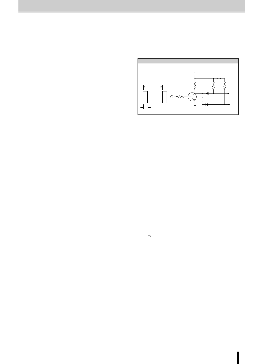
65
A3953SB/SLB
2-Phase Stepper Motor Bipolar Driver ICs (2-Phase/1-2 Phase Excitation)
A3953SB/SLB
100 k
Ω
20 k
Ω
1N4001
2N2222
V
CC
RC
1
RC
N
t
1
t
2
Fig. 3 Synchronous Fixed-Frequency Control Circuit
Set V
REF
to 0 volts. With the load connected and the PWM cur-
rent control operating in slow current-decay mode, use and os-
cilloscope to measure the time the output is low (sink ON) for
the output that is chopping. This is the typical minimum ON
time (t
ON (min)
typ) for the device.
The C
T
then should be increased until the measured value of t
ON
(min)
is equal to t
ON (min)
max as specified in the electrical charac-
teristics table. When the new value of C
T
has been set, the value
of R
T
should be decreased so the value for t
OFF
=R
T
•
C
T
(with the
artificially increased value of C
T
) is equal to the nominal design
value. The worst-case load-current regulation then can be mea-
sured in the system under operating conditions.
(F) PWM of the PHASE and ENABLE Inputs.
The PHASE and ENABLE inputs can be pulse-width modulated
to regulate load current. Typical propagation delays from the
PHASE and ENABLE inputs to transitions of the power outputs
are specified in the electrical characteristics table. If the internal
PWM current control is used, the comparator blanking function
is active during phase and enable transitions. This eliminates
false tripping of the over-current comparator caused by switch-
ing transients (see “RC Blanking” above).
(1) Enable PWM.
With the MODE input low, toggling the ENABLE input turns ON
and OFF the selected source and sink drivers. The correspond-
ing pair of flyback and ground-clamp diodes conduct after the
drivers are disabled, resulting in fast current decay. When the
device is enabled the internal current-control curcuitry will be
active and can be used to limit the load current in a slow cur-
rent-decay mode.
For applications that PWM the ENABLE input and desire the
internal current-limiting circuit to function in the fast decay mode,
the ENABLE input signal should be inverted and connected to
the MODE input. This prevents the device from being switched
into sleep mode when the ENABLE input is low.
(2) Phase PWM.
Toggling the PHASE terminal selects which sink/source pair is
enabled, producing a load current that varies with the duty cycle
and remains continuous at all times. This can have added ben-
efits in bidirectional brush dc servo motor applications as the
transfer function between the duty cycle on the PHASE input
and the average voltage applied to the motor is more linear
than in the case of ENABLE PWM control (withch produces a
discontinuous current at low current levels). For more informa-
tion see “DC Motor Applications” below.
(3) Synchronous Fixed-Frequency PWM.
The internal PWM current-control circuitry of multiple A3953S-
devices can be synchronized by using the simple circuit shown
in figure 3. A 555IC can be used to generate the reset pulse/
blanking signal (t
1
) for the device and the period of the PWM
cycle (t
2
). The value of t
1
should be a minimum of 1.5ms. When
used in this configuration, the R
T
and C
T
components should be
omitted. The PHASE and ENABLE inputs should not be PWM
with this circuit configuration due to the absence of a blanking
function synchronous with their transitions.
(G)Miscellaneous Information.
A logic high applied to both the ENABLE and MODE terminals
puts the device into a sleep mode to minimize current consump-
tion when not in use.
An internally generated dead time prevents crossover currents
that can occur when switching phase or braking.
Thermal protection circuitry turns OFF all drivers should the junc-
tion termperature reach 165
°
C (typical). This is intended only to
protect the device from failures due to excessive junction tem-
peratures and should not imply that output short circuits are
permitted. The hysteresis of the thermal shutdown circuit is ap-
proximately 8
°
C.
■
APPLICATION NOTES
(A)Current Sensing.
The actual peak load current (I
PEAK
) will be above the calculated
value of I
TRIP
due to delays in the turn off of the drivers. The
amount of overshoot can be approximated by:
where V
BB
is the motor supply voltage, V
BEMF
is the back-EMF
voltage of the load, R
LOAD
and L
LOAD
are the resistance and in-
ductance of the load respectively, and t
PWM (OFF)
is specified in
the electrical characteristics table.
The reference terminal has a maximum input bias current of
±
5
µ
A. This current should be taken into account when deter-
mining the impedance of the external circuit that sets the refer-
ence voltage value.
To minimize current-sensing inaccuracies caused by ground
trace I
•
R drops, the current-sensing resistor should have a sepa-
rate return to the ground terminal of the device. For low-value
sense resistors, the I
•
R drops in the printed wiring board can be
significant and should be taken into account. The use of sock-
ets should be avoided as their contact resistance can cause
variations in the effective value of R
S
.
Generally, larger values of R
S
reduce the aforementioned ef-
fects but can result in excessive heating and power loss in the
I
OS
L
LOAD
(V
BB-
[(I
TRIP
•
R
LOAD
) + V
BEMF
])
•
t
PWM (OFF)
ac/Allegro/Allegro_Motor_Drive_ICs-html.html
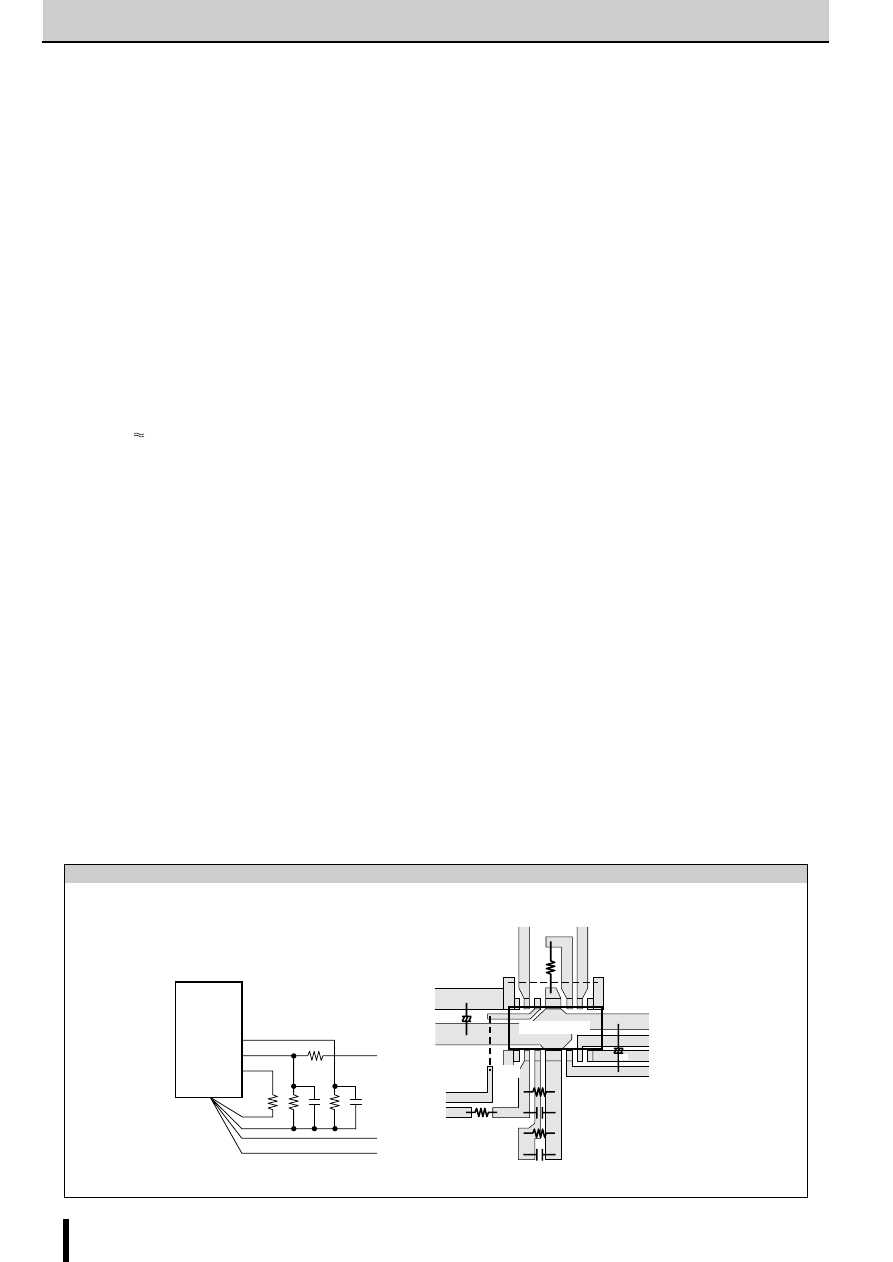
66
A3953SB/SLB
2-Phase Stepper Motor Bipolar Driver ICs (2-Phase/1-2 Phase Excitation)
A3953SB/SLB
Fig. 4 Example of Circuit (including GND) and GND Wiring Pattern
T
J
T
TAB
+ (I
LOAD
•
2
•
V
F
•
R
JT
)
θ
Use jumper wiring
for dotted line.
A3953SLB
4, 5,
12, 13
R
S
RC
REF
SENSE
V
CC
GND
V
CC
GND
V
BB
GND
Rt
Rt
Ct
Ct
Vref
Vref
V
BB
OUT
A
OUT
B
V
CC
V
BB
GND
Phase
Enable
Mode
+
+
1Pin
A3953SLB
sense resistor. The selected value of R
S
should not cause the
absolute maximum voltage rating of 1.0V (0.4V for
V
CC
=3.3Voperation), for the SENSE terminal, to be exceeded.
The current-sensing comparator functions down to ground al-
lowing the device to be used in microstepping, sinusoidal, and
other varying current-profile applications.
(B) Thermal Considerations.
For reliable operation it is recommended that the maximum junc-
tion termperature be kept below 110
°
C to 125
°
C. The junction
termperature can be measured best by attaching a thermocouple
to the power tab/batwing of the device and measuring the tab
temperature, T
TAB
. Tthe junction temperature can then be ap-
proximated by using the formula:
where V
F
may be chosen from the electrical specification table
for the given level of I
LOAD
. The value for R
θ
JT
is given in the
package thermal resistance table for the appropriate package.
The power dissipation of the batwing packages can be improved
by 20% to 30% by adding a section of printed circuit board cop-
per (typically 6 to 18 square centimeters) connected to the
batwing terminals of the device.
The thermal performance in applications that run at high load
currents and/or high duty cycles can be improved by adding
external diodes in parallel with the internal diodes. In internal
PWM slow-decay applications, only the two ground clamp di-
odes need be added. For internal fast-decay PWM, or external
PHASE or ENABLE input PWM applications, all four external
diodes should be added for maximum junction temperature re-
duction.
(C)PCB Layout.
The load supply terminal, V
BB
should be decoupled with an elec-
trolytic capacitor (>47
µ
F is recommeded) placed as close to the
device as is physically practical. To minimize the elffect of sys-
tem ground I
•
R drops on the logic and reference input signals,
the system ground should have a low-resistance return to the
motor supply voltage.
See also “Current Sensing” and “Thermal Considerations” above.
(D)Fixed Off-Time Selection.
With increasing values of t
OFF
, switching losses will decrease,
low-level load-current regulation will improve, EMI will be re-
duced, the PWM frequency will decrease, and ripple current will
increase. The value of t
OFF
can be chosen for optimization of
these parameters. For applications where audible noise is a
concern, typical values of t
OFF
are chosen to be in the range of
15 ms to 35 ms.
(E) Stepper Motor Applications.
The MODE terminal can be used to optimize the performance
of the device in microstepping/sinusoidal stepper-motor drive
applications. When the load current is increasing, slow decay
mode is used to limit the switching losses in the device and iron
losses in the motor. This also improves the maximum rate at
which the load current can increase (as compared to fast de-
cay) due to the slow rate of decay during t
OFF
.
When the load current is decreasing, fast-decay mode is used
to regulate the load current to the desired level. This prevents
tailing of the current profile caused by the back-EMF voltage of
the stepper motor.
ac/Allegro/Allegro_Motor_Drive_ICs-html.html

67
A3953SB/SLB
2-Phase Stepper Motor Bipolar Driver ICs (2-Phase/1-2 Phase Excitation)
A3953SB/SLB
In stepper-motor applications applying a constant current to the
load, slow-decay mode PWM is typically used to limit the switch-
ing lossess in the device and iron losses in the motor.
(F) DC Motor Applications.
In closed-loop systems, the speed of a dc motor can be con-
trolled by PWM of the PHASE or ENABLE inputs, or by varying
the reference input voltage (REF). In digital systems (micropro-
cessor controlled), PWM of the PHASE or ENABLE input is used
typically thus avoiding the need to generate a variable analog
voltage reference. In this case, a dc voltage on the REF input is
used typically to limit the maximum load current.
In dc servo applications, which require accurate positioning at
low or zero speed, PWM of the PHASE input is selected typi-
cally. This simplifies the servo control loop because the transfer
function between the duty cycle on the PHASE input and the
average voltage applied to the motor is more linear than in the
case of ENABLE PWM comtrol (which produces a discontinu-
ous current at low current levels).
With bidirectional dc servo motors, the PHASE terminal can be
used for mechanical direction control. Similar to when branking
the motor dynamically, abrupt changes in the direction of a ro-
tating motor produces a current generated by the back-EMF.
The current generated will depend on the mode of operation. If
the internal current control circuitry is not being used, then the
maximum load current generated can be approximated by
I
LOAD
=(V
BEMF
+V
BB
)/R
LOAD
where V
BEMF
is proportional to the motor’s
speed. If the internal slow current-decay control circuitry is used,
then the maximum load current generated can be approximated
by I
LOAD
=V
BEMF
/R
LOAD
. For both cases care must be taken to en-
sure that the maximum ratings of the device are not exceeded.
If the internal fast current-decay control circuitry is used, then
the load current will regulate to a value given by:
CAUTION: In fast current-decay mode, when the direction of
the motor is changed abruptly, the kinetic energy stored in the
motor and load inertia will be converted into current that charges
the V
BB
supply bulk capacitance (power supply output and
decoupling capacitance). Care must be taken to ensure that the
capacitance is sufficient to absorb the energy without exceed-
ing the voltage rating of any devices connected to the motor
supply.
See also “Brake Operation” above.
I
LOAD
R
S
V
REF
ac/Allegro/Allegro_Motor_Drive_ICs-html.html
68
A2918SW
2-Phase Stepper Motor Bipolar Driver IC
A2918SW
Allegro MicroSystems product
■
Features
●
Fixed off-time PWM current control
●
Low saturation voltage (Sink transistor)
●
Internal thermal shutdown circuitry
●
Internal crossover-current protection cir-
cuitry
●
Internal UVLO protection
●
Internal transient-suppression diodes
●
Low thermal resistance 18-pin SIP
■
Absolute Maximum Ratings
Parameter
Symbol
Conditions
Ratings
Units
Motor supply voltage
V
BB
45
V
Output current (peak)
I
O (peak)
tw
≤
20
µ
s
±
1.75
A
Output current (continuous)
I
O
±
1.5
A
Logic supply voltage
V
CC
7.0
V
Logic input voltage range
V
IN
−
0.3 to +7.0
V
Output emitter voltage
V
E
1.5
V
Package power dissipation
P
D
(Note1)
4.0
W
Operating temperature
T
a
−
20 to +85
°
C
Junction temperature
T
j
(Note2)
+150
°
C
Storage temperature
T
stg
−
55 to +150
°
C
●
Output current rating may be limited by duty cycle, ambient temperature, and heat sinking. Under any
set of conditions, do not exceed the specified current rating or a junction temperature of 150
°
C.
Note 1: When ambient temperature is 25
°
C or over, derate using
−
32.0mW/
°
C.
Note 2: Fault conditions where junction temperature (T
j
) exceeds 150
°
C will activate the device’s thermal
shutdown circuitry. These conditions can be tolerated but should be avoided.
■
Electrical Characteristics
Parameter
Symbol
Conditions
Limits
Units
min
typ
max
Power outputs (OUT
A
or OUT
B
)
Motor supply voltage range
V
BB
10
45
V
Output leakage current
I
CEX
V
O
=V
BB
50
µ
A
V
O
=0V
−
50
µ
A
Output saturation voltage
V
CE (SUS)
I
O
=
±
1.5A, L=3.5mH
45
V
Sink driver, I
O
=+1.0A
0.8
V
Output sustaining voltage
V
CE (SAT)
Sink driver, I
O
=+1.5A
1.1
V
Source driver, I
O
=
−
1.0A
2.0
V
Source driver, I
O
=
−
1.5A
2.2
V
Clamp diode leakage current
I
R
V
R
=45V
50
µ
A
Clamp diode forward voltage
V
F
I
F
=1.5A
2.0
V
Motor supply current
I
BB (ON)
Both bridges ON, no load
15
mA
I
BB (OFF)
Both bridges OFF
10
mA
Control logic
Input voltage
V
IH
All inputs
2.4
V
V
IL
All inputs
0.8
V
Input current
I
IH
V
IN
=2.4V
20
µ
A
I
IL
V
IN
=0.8V
−
200
µ
A
Reference voltage range
V
REF
Operating
1.5
V
CC
V
Current control threshold
V
REF
/V
SENSE
V
REF
=5V
9.5
10
10.5
Thermal shutdown temperature
T
j
170
°
C
Logic supply current
I
CC
V
EN
=0.8V, no load
140
mA
●
“typ” values are for reference.
(Unless specified otherwise, T
a
=25
°
C, V
BB
=45V, V
CC
=4.75V to 5.25V, V
REF
=5V)
■
Terminal Connection Diagram
OUT
1A
OUT
2A
OUT
2B
OUT
1B
LOAD SUPPLY
E
2
SENSE
2
SENSE
1
E
1
PHASE
2
PHASE
1
REFERENCE
RC
2
RC
1
V
CC
V
BB
1
2
V
REF
PWM1
TSD
GROUND
LOGIC SUPPLY
ENABLE
2
ENABLE
1
PWM2
1
2
3
4
5
6
7
8
9
10
11
12
13
14
15
16
17
18
■
Derating
4
5
3
2
1
0
−
20
0
25
50
75
100
85
Ambient temperature Ta (C
°
)
Allowable package power dissipation P
D
(W)
31.25C
°
/ W
2-Phase/1-2 Phase Excitation
ac/Allegro/Allegro_Motor_Drive_ICs-html.html
69
A2918SW
2-Phase Stepper Motor Bipolar Driver IC (2-Phase/1-2 Phase Excitation)
A2918SW
■
Truth Table
■
Internal Block Diagram
■
External Dimensions
Plastic SIP
ENABLE
PHASE
OUT
A
OUT
B
L
L
H
H
L
X
H
L
Z
L
H
Z
X=Don't Care Z=High impedance
3()
6.7
±
0.5
1 2 3
18
31.3
±
0.2
1
0.2
0.1
0.65
0.2
0.1
31
±
0.2
24.4
±
0.2
16.4
±
0.2
3.2
±
0.15
4
±
0.7
0.55
0.2
0.1
9.7
1 0.5
2.45
±
0.2
1.7
4.8
±
0.2
±
0.1
R-End
9.9
16
±
0.2
13
±
0.2
±
0.2
+
---
+
---
28.56
±
1
P1.68
17
±
0.7
×
=
3.2
±
0.15
3.8
×
+
---
+ ---
31.3
±
0.2
0.65
0.2
0.1
+
---
1
0.2
0.1
+
---
28.56
±
1
P1.68
17
±
0.4
×
=
1 2 3
18
2.2
±
0.1
1.6
±
0.6
4.6
±
0.6
3.0
±
0.6
7.5
±
0.6
6.0
±
0.6
0.55
0.2 0.1
+ ---
31
±
0.2
24.4
±
0.2
16.4
±
0.2
3.2
±
0.15
2.45
±
0.2
1.7
4.8
±
0.2
±
0.1
9.9
16
±
0.2
13
±
0.2
±
0.2
3.2
±
0.15
3.8
×
A2918SWV
A2918SWH
(Unit: mm)
SOURCE
DISABLE
LOGIC
SUPPLY
LOAD
SUPPLY
V
CC
V
BB
OUT
1A
OUT
2A
OUT
2B
OUT
1B
TSD
PWM2
PWM1
PHASE
1
ENABLE
1
R
T
C
T
C
C
C
C
C
T
R
C
R
C
R
S
R
S
R
T
RC
1
SENSE
1
SENSE
2
RC
2
REFERENCE
GROUND
E
1
E
2
V
REF
PHASE
2
ENABLE
2
1
2
11
1
17
5
2
4
8
7
13
14
ONE SHOT
SOURCE
DISABLE
ONE SHOT
9
6
3
10
15
18
16
12
+
−
+
−
÷
10
÷
10
ICs per stick
18
φ
φ
φ
φ
ac/Allegro/Allegro_Motor_Drive_ICs-html.html
70
A3952SB/SLB/SW
2-Phase Stepper Motor Bipolar Driver ICs
A3952SB/SLB/SW
■
Features
●
Fixed off-time PWM current control
●
Switching between power supply regenera-
tion mode and loop regeneration mode in
order to improve motor current response in
microstepping
●
External filter for sense terminal not required
●
Sleep (low current consumption) mode
●
Brake operation with PWM current limiting
●
Internal thermal shutdown circuitry
●
Internal crossover-current protection circuitry
●
Internal UVLO protection
●
Internal transient-suppression diodes
●
Low thermal resistance package
■
Electrical Characteristics
■
Absolute Maximum Ratings
Parameter
Symbol
Conditions
Ratings
Units
A3952SB A3952SLB A3952SW
Load supply voltage
V
BB
50
V
Output current (peak)
I
O (Peak)
tw
≤
20
µ
s
±
3.5
A
Output current (continuous)
I
O
±
2.0
A
Logic supply voltage
V
CC
7.0
V
Logic input voltage
V
IN
−
0.3 to V
CC
+0.3
V
Sense voltage
V
SENSE
1.5
V
Reference voltage
V
REF
15
V
Package power dissipation
P
D
(Note1)
2.90
1.86
3.47
W
Operating temperature
T
a
−
20 to +85
°
C
Junction temperature
T
j
(Note2)
+150
°
C
Storage temperature
T
stg
−
55 to +150
°
C
●
Output current rating may be limited by duty cycle, ambient temperature, and heat sinking. Under any
set of conditions, do not exceed the specified current rating or a junction temperature of 150
°
C.
Note 1: When ambient temperature is 25
°
C or over, derate using
−
23.26mW/
°
C(SB),
−
14.93mW/
°
C(SLB)
or
−
27.78mW/
°
C(SW).
Note 2: Fault conditions where junction temperature (T
j
) exceeds 150
°
C will activate the device’s thermal
shutdown circuitry. These conditions can be tolerated but should be avoided.
(Unless specified otherwise, T
a
=25
°
C, V
BB
=50V, VC
C
=5.0V, V
BRAKE
=2.0V, V
SENSE
= 0V, 20k
Ω
& 1000pF RC to ground)
Parameter
Symbol
Conditions
Limits
Units
min
typ
max
Power outputs
Load supply voltage range
V
BB
Operating, I
O
=
±
2.0A, L=3mH
V
CC
50
V
Output leakage current
I
CEX
V
O
=V
BB
<1.0
50
µ
A
V
O
=0V
<
−
1.0
−
50
µ
A
Source driver, I
O
=
−
0.5A
0.9
1.2
V
Source driver, I
O
=
−
1.0A
1.0
1.4
V
Output saturation voltage
V
CE (SAT)
Source driver, I
O
=
−
2.0A
1.2
1.8
V
Sink driver, I
O
=+0.5A
0.9
1.2
V
Sink driver, I
O
=+1.0A
1.0
1.4
V
Sink driver, I
O
=+2.0A
1.3
1.8
V
Clamp diode forward voltage
I
F
=0.5A
1.0
1.4
V
(Source or sink)
V
F
I
F
=1.0A
1.1
1.6
V
I
F
=2.0A
1.4
2.0
V
I
BB (ON)
V
ENABLE
=0.8V, V
BRAKE
=2.0V
2.9
6.0
mA
Load supply current
I
BB (OFF)
V
ENABLE
=2.0V, V
MODE
=0.8V, V
BRAKE
=2.0V
3.1
6.5
mA
(No load)
I
BB (BRAKE)
V
BRAKE
=2.0V
3.1
6.5
mA
I
BB (SLEEP)
V
ENABLE
=V
MODE
=V
BRAKE
=2.0V
<1.0
50
µ
A
Control logic
Logic supply voltage range
V
CC
Operating
4.5
5.0
5.5
V
Logic input voltage
V
IH
2.0
V
V
IL
0.8
V
Logic input current
I
IH
V
IH
=2.0V
<1.0
20
µ
A
I
IL
V
IL
=0.8V
<
−
2.0
−
200
µ
A
Reference voltage range
V
REF
Operating
0
15
V
Reference input current
I
REF
V
REF
=2.0V
25
40
55
µ
A
Reference voltage divider ratio
V
REF
=15V
9.5
10.0
10.5
Comparator input offset voltage
V
IO
V
REF
=0V
±
1.0
±
10
mV
PWM RC fixed off-time
t
off
C
T
=1000pF, R
T
=20k
Ω
18
20
22
µ
s
PWM minimum on-time
t
on (min)
C
T
=820pF, R
T
≥
12k
Ω
1.7
3.0
µ
s
C
T
=1200pF, R
T
≥
12k
Ω
2.5
3.8
µ
s
I
OUT
=
±
2.0A, 50% E
IN
to 90% E
out
Transition:
ENABLE ON to SOURCE ON
2.9
µ
s
ENABLE OFF to SOURCE OFF
0.7
µ
s
ENABLE ON to SINK ON
2.4
µ
s
Propagation delay time
t
pd
ENABLE OFF to SINK OFF
0.7
µ
s
PHASE CHANGE to SOURCE ON
2.9
µ
s
PHASE CHANGE to SOURCE OFF
0.7
µ
s
PHASE CHANGE to SINK ON
2.4
µ
s
PHASE CHANGE to SINK OFF
0.7
µ
s
t
pd (PWM)
Comparator Trip to SINK OFF
0.8
1.5
µ
s
Thermal shutdown temperature
T
j
165
°
C
Thermal shutdown hysteresis
∆
T
j
15
°
C
UVLO enable threshold
V
CC (UVLO)
3.15
3.50
3.85
V
UVLO hysteresis
∆
V
CC (UVLO)
300
400
500
mV
I
CC (ON)
V
ENABLE
=0.8V, V
BRAKE
=2.0V
20
30
mA
Logic supply current
I
CC (OFF)
V
ENABLE
=2.0V, V
MODE
=0.8V, V
BRAKE
=2.0V
12
18
mA
(No load)
I
CC (BRAKE)
V
BRAKE
=0.8V
26
40
mA
I
CC (SLEEP)
V
ENABLE
=V
MODE
=V
BRAKE
=2.0V
3.0
5.0
mA
●
“typ” values are for reference.
Allegro MicroSystems product
2-Phase/1-2 Phase Excitation
ac/Allegro/Allegro_Motor_Drive_ICs-html.html
71
A3952SB/SLB/SW
2-Phase Stepper Motor Bipolar Driver ICs (2-Phase/1-2 Phase Excitation)
A3952SB/SLB/SW
■
Derating
■
Internal Block Diagram
■
Truth Table
■
External Dimensions
(Unit: mm)
■
Terminal Connection Diagram
Plastic DIP
(300mil)
Wide body plastic SOP
(300mil)
Plastic power SIP
ENABLE
BRAKE
PHASE
MODE
Operating Mode
OUT
A
OUT
B
H
H
H
H
H
H
L
L
H
H
L
L
L
L
X
X
X
X
H
H
L
L
X
X
H
L
H
L
H
L
H
L
Z
Z
H
H
L
L
L
L
Z
Z
L
L
H
H
L
L
Sleep mode
Standby
(Note 1)
Forward, fast current-decay mode
Forward, slow current-decay mode
Reverse, fast current-decay mode
Reverse, slow current-decay mode
Brake, fast current-decay mode
Brake, no current control
(Note 2)
BRAKE
PHASE
LOGIC
V
CC
V
BB
MODE
1
2
3
4
5
6
7
8
9
10
11
13
12
14
15
16
V
BB
LOAD
SUPPLY
OUT
B
GROUND
GROUND
SENSE
OUT
A
LOAD
SUPPLY
REF
RC
GROUND
GROUND
LOGIC
SUPPLY
ENABLE
BRAKE
PHASE
LOGIC
V
CC
V
BB
MODE
1
2
3
4
5
6
7
8
9
10
11
13
12
14
15
16
V
BB
LOAD
SUPPLY
OUT
B
GROUND
GROUND
SENSE
OUT
A
LOAD
SUPPLY
REF
RC
GROUND
GROUND
LOGIC
SUPPLY
ENABLE
PHASE
MODE
BRAKE
REF
RC
LOAD
SUPPLY
LOGIC
SUPPLY
OUT
A
SENSE
ENABLE
10
9
8
7
6
5
4
1
3
2
12
11
LOGIC
GROUND
OUT
B
V
BB
V
CC
0
−
20
0
25
50
75
100
85
A3952SW 36
°
C/W
1
2
3
4
5
A3952SB 43
°
C/
W
A3952S
LB 67
°
C/ W
Ambient temperatureTa (
°
C)
Allowable package power dissipation P
D
(W)
1.27
0.40
0.32
0.23
10.65
10.00
7.60
7.40
10.50
10.10
0.51
0.33
1
8
9
16
2.65
2.35
SEATING PLANE
0.10 MIN.
1.27
BSC
0
°
TO 8
°
MODE
PHASE
ENABLE
BRAKE
LOGIC
SUPPLY
V
CC
REF
9R
R
GROUND
1.5V
V
CC
BLANKING
PWM LATCH
Q
R
S
+
−
−
+
V
TH
SENSE
"B", "LB" , & "W"
PACKAGES
RC
R
S
R
T
C
T
EMITTERS
"EB" ONLY
OUT
B
LOAD
SUPPLY
V
BB
OUT
A
SLEEP &
STANDBY MODES
UVLO
& TSD
INPUT LOGIC
1.77
1
2
3
8
9
16
1.15
21.33
18.93
0.558
0.356
4.06
2.93
7.11
6.10
INDEX AREA
0.127MIN
7.62BSC
2.54BSC
5.33MAX
SEATING PLANE
0.39MIN
0.381
0.204
●
Thickness of lead is measured below seating plane.
●
Allowable variation in distance between leads is not cumulative.
Lead width of pin 1, 8, 9, 16 may be half the value shown here.
Maximum thickness of lead is 0.508mm.
Note 1:
2:
ICs per stick
25
ICs per stick
47
ICs per stick
15
A3952SB
A3952SLB
A3952SW
A3952SB
A3952SLB
A3952SW
Don't Care
High impedance
Includes active pull-offs for power outputs
Includes internal default
V
SENSE
level for overcurrent protection
X :
Z :
Note 1:
Note 2:
●
Thickness of lead is measured below seating plane.
●
Allowable variation in distance between leads is not cumulative.
●
Lead is measured 0.762mm below seating plane.
4.57MAX
1.40
1.14
3.43
2.54
2.03
1.78
0.59
0.46
0.76
0.51
19.69
19.43
32.00
31.50
1.65
0.89
3.94
3.68
6.22
5.71
14.48
13.72
3.56
9.27
7.37MIN
SEATING
PLANE
2.54
±
0.25
1
2
3
12
INDEX
AREA
0.51
φ
ac/Allegro/Allegro_Motor_Drive_ICs-html.html
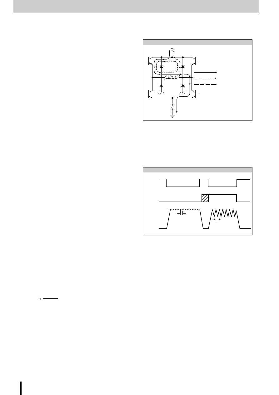
72
A3952SB/SLB/SW
2-Phase Stepper Motor Bipolar Driver ICs (2-Phase/1-2 Phase Excitation)
A3952SB/SLB/SW
■
Outline
Designed for bidirectional pulse-width modulated current con-
trol of inductive loads, the A3952S- is capable of continuous
output currents to
±
2A and operating voltages to 50V. Internal
fixed off-time PWM current-control circuitry can be used to regu-
late the maximum load current to a desired value. The peak
load current limit is set by the user’s selection of an input refer-
ence voltage and external sensing resistor. The fixed OFF-time
pulse duration is set by a user-selected external RC timing net-
work. Internal circuit protection includes thermal shutdown with
hysteresis, transient suppression diodes, and crossover-current
protection. Special power-up sequencing is not required.
With the ENABLE input held low, the PHASE input controls load
current polarity by selecting the appropriate source and sink
driver pair. The MODE input determines whether the PWM cur-
rent-control circuitry operates in a slow current-decay mode (only
the selected sink driver switching) or in a fast current-decay
mode (selected source and sink switching). A user-selectable
blanking window prevents false triggering of the PWM current
control circuitry. With the ENABLE input held high, all output
drivers are disabled. A sleep mode is provided to reduce power
consumption when inactive.
When a logic low is applied to the BRAKE input, the braking
function is enabled. This overrides ENABLE and PHASE to turn
OFF both source drivers and turn ON both sink drivers. The
brake function can be safely used to dynamically brake brush
dc motors.
■
FUNCTIONAL DESCRIPTION
(A) INTERNAL PWM CURRENT CONTROL DURING FOR-
WARD AND REVERSE OPERATION
The A3952S- contains a fixed OFF-time pulse-width modulated
(PWM) current-control circuit that can be used to limit the load
current to a desired value. The value of the current limiting (I
TRIP
)
is set by the selection of an external current sensing resistor
(R
S
) and reference input voltage (V
REF
). The internal circuitry
compares the voltage across the external sense resistor to one
tenth the voltage on the REF input terminal, resulting in a func-
tion approximated by
In forward or reverse mode the current-control circuitry limits
the load current. When the load current reaches I
TRIP
, the com-
parator resets a latch to turn OFF the selected sink driver (in the
slow-decay mode) or selected sink and source driver pair (in
the fast-decay mode). In slow-decay mode, the selected sink
driver is disabled; the load inductance causes the current to
recirculate through the source driver and flyback diode (see fig-
ure 1). In fast-decay mode, the selected sink and source driver
pair are disabled; the load inductance causes the current to flow
from ground to the load supply via the ground clamp and flyback
diodes.
Fig. 1 Load-Current Paths
R
S
V
BB
DRIVE CURRENT
RECIRCULATION (SLOW-DECAY MODE)
RECIRCULATION (FAST-DECAY MODE)
Fig. 2 Fast and Slow Current-Decay Waveforms
ENABLE
MODE
LOAD
CURRENT
RC
I
TRIP
RC
I
TRIP
10
•
R
S
V
REF
Application Notes
The user selects an external resistor (R
T
) and capacitor (C
T
) to
determine the time period (t
off
=R
T
C
T
) during which the drivers
remain disabled (see “RC Fixed OFF Time” below). At the end
of the R
T
C
T
interval, the drivers are re-enabled allowing the load
current to increase again. The PWM cycle repeats, maintaining
the load current at the desired value (see figure 2).
(B)INTERNAL PWM CURRENT CONTROL DURING BRAKE
MODE OPERATION
The brake circuit turns OFF both source drivers and turns ON
both sink drivers. For dc motor applications, this has the effect
of shorting the motor’s back-EMF voltage, resulting in current
flow that brakes the motor dynamically. However, if the back-
EMF voltage is large, and there is no PWM current limiting, then
the load current can increase to a value that approaches a locked
rotor condition. To limit the current, when the I
TRIP
level is reached,
the PWM circuit disables the conducting sink driver. The energy
stored in the motor’s inductance is then discharged into the load
supply causing the motor current to decay.
As in the case of forward/reverse operation, the drivers are re-
enabled after a time given by t
off
=R
T
•
C
T
(see”RC Fixed OFF Time”
below). Depending on the back-EMF voltage (proportional to
the motor’s decreasing speed), the load current again may in-
crease to I
TRIP
. If so, the PWM cycle will repeat, limiting the load
current to the desired value.
(1) Brake Operation-MODE Input High
During braking, when the MODE input is high, the current limit
can be approximated by
ac/Allegro/Allegro_Motor_Drive_ICs-html.html

73
A3952SB/SLB/SW
2-Phase Stepper Motor Bipolar Driver ICs (2-Phase/1-2 Phase Excitation)
A3952SB/SLB/SW
I
TRIP
10
•
R
S
V
REF
I
TRIP
R
S
1.5V
t
OFF
R
T
•
C
T
CAUTION: Because the kinetic energy stored in the motor and
load inertia is being converted into current, which charges the
V
BB
supply bulk capacitance (power supply output and
decoupling capacitance), care must be taken to ensure the ca-
pacitance is sufficient to absorb the energy without exceed-
ing the voltage rating of any devices connected to the motor
supply.
(2) Brake Operation-MODE Input Low
During braking,with the MODE input low, the peak current limit
defaults internally to a value approximated by
In this mode, the value of R
S
determines the I
TRIP
value indepen-
dent of V
REF
. This is useful in applicaions with differing run and
brake currents and no practical method of varying V
REF
.
Choosing a small value for R
S
essentially disables the current
limiting during braking. Therefore, care should be taken to en-
sure that the motor’s current does not exceed the absolute
maximum ratings of the device. The braking current can be
measured by using an oscilloscope with a current probe con-
nected to one of the motor’s leads.
(C) RC Fixed OFF Time
The internal PWM current control circuitry uses a one shot to
control the time the driver (s) remain (s) OFF. The one shot
time, t
off
(fixed OFF time), is determined by the selection of an
external resistor (R
T
) and capacitor (C
T
) connected in parallel
from the RC terminal to ground. The fixed OFF time, over a
range of values of C
T
=820pF to 1500pF and R
T
=12k
Ω
to 100k
Ω
,
is approximated by
When the PWM latch is reset by the current comparator, the
voltage on the RC terminal will begin to decay from approxi-
mately 3 volts. When the voltage on the RC terminal reaches
approximately 1.1 volt, the PWM latch is set, thereby re-enabling
the driver (s).
(D) RC Blanking
In addition to determining the fixed OFF-time of the PWM con-
trol circuit, the C
T
component sets the comparator blanking time.
This function blanks the output of the comparator when the out-
puts are switched by the internal current control circuitry (or by
the PHASE, BRAKE, or ENABLE inputs). The comparator out-
put is blanked to prevent false over-current detections due to
reverse recovery currents of the clamp diodes, and/or switching
transients related to distributed capacitance in the load.
During internal PWM operation, at the end of the t
off
time, the
comparator’s output is blanked and C
T
begins to be charged
from approximately 1.1V by an internal current source of ap-
proximately 1mA. The comparator output remains blanked until
the voltage on C
T
reaches approximately 3.0 volts.
Similarly, when a transition of the PHASE input occurs, C
T
is
discharged to near ground during the crossover delay time (the
crossover delay time is present to prevent simultaneous con-
duction of the source and sink drivers). After the crossover de-
lay, C
T
is charged by an internal current source of approximately
1mA. The comparator output remains blanked until the voltage
on C
T
reaches approximately 3.0 volts.
Similarly, when the device is disabled via the ENABLE input, C
T
is discharged to near ground. When the device is re-enabled,
C
T
is charged by the internal current source. The comparator
output remains blanked until the voltage on C
T
reaches approxi-
mately 3.0V.
For applications that use the internal fast-decay mode PWM
operation, the minimum recommended value is C
T
=1200pF
±
5%.
For all other applications, the minimum recommended value is
C
T
=820pF
±
5%. These values ensure that the blanking time is
sufficient to avoid false trips of the comparator under normal
operating conditions. For optimal regulation of the load current,
the above values for C
T
are recommended and the value of R
T
can be sized to determine t
off
. For more information regarding
load current regulation, see below.
(E) LOAD CURRENT REGULATION WITH THE INTERNAL
PWM CURRENT-CONTROL CIRCUITRY
When the device is operating in slow-decay mode, there is a
limit to the lowest level that the PWM current-control circuitry
can regulate load current. The limitation is the minimum duty
cycle, which is a function of the user-selected value of t
off
and
the maxuimum value of the minimum ON-time pulse, t
on (min)
, that
occurs each time the PWM latch is reset. If the motor is not
rotating, as in the case of a stepper motor in hold/detent mode,
or a brush dc motor when stalled or at startup, the worst-case
value of current regulation can be approximated by
where t
off
=R
T
•
C
T
, R
LOAD
is the series resistance of the load, V
BB
is
the load/motor supply voltage, and t
on (min)
max is specified in the
electrical characteristics table. When the motor is rotating, the
back EMF generated will influence the above relationship. For
brush dc motor applications, the current regulation is improved.
For stepper motor applications when the motor is rotating, the
effect is more complex. A discussion of this subject is included
in the section on stepper motors under “Applications”.
The following procedure can be used to evaluate the worst-case
slow-decay internal PWM load current regulation in the system:
Set V
REF
to 0 volts. With the load connected and the PWM current
control operating in slow-decay mode, use an oscilloscope to
measure the time the output is low (sink ON) for the output that is
chopping. This is the typical minimum ON time (t
on (min)
typ) for the
1.05
•
(t
on (min)
max + t
off
)
•
R
LOAD
[(V
BB
−
V
SAT (source
+
sink)
)
•
t
on (min)
max]
−
[1.05
•
(V
SAT (sink)
+ V
D
)
•
t
off
]
I
(AV)
≅
ac/Allegro/Allegro_Motor_Drive_ICs-html.html
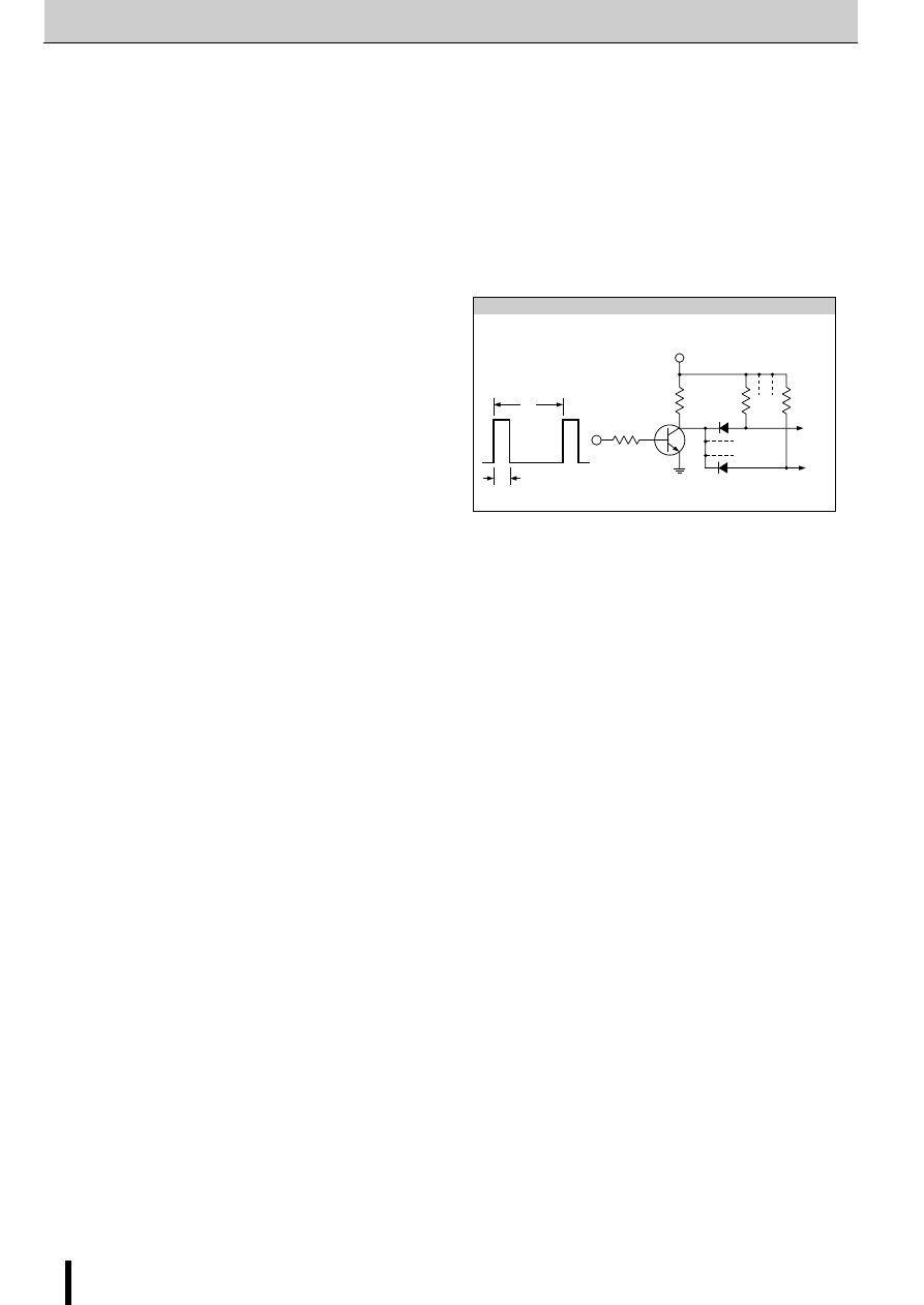
74
A3952SB/SLB/SW
2-Phase Stepper Motor Bipolar Driver ICs (2-Phase/1-2 Phase Excitation)
A3952SB/SLB/SW
100 k
Ω
20 k
Ω
1N4001
2N2222
V
CC
RC
1
RC
N
t
1
t
2
Fig. 3 Synchronous Fixed-Frequency Control Circuit
device. C
T
then should be increased until the measured value
of t
on (min)
is equal to t
on (min)
max)=3.0
µ
s as specified in the electri-
cal characteristics table. When the new value of C
T
has been
set, the value of R
T
should be decreased so the value for
t
off
=R
T
•
C
T
(with the artificially increased value of C
T
) is equal to
105% of the nominal design value. The worst-case load current
regulation then can be measured in the system under operating
conditions.
In applications utilizing both fast-and slow-decay internal PWM
modes, the performance of the slow-decay current regulation
should be evaluated per the above procedure and a t
on (min)
max
of 3.8
µ
s. This corresponds to a C
T
value of 1200pF, which is
required to ensure sufficient blanking during fast-decay internal
PWM.
(F) LOAD CURRENT REGULATION WITH EXTERNAL PWM
OF THE PHASE AND ENABLE INPUTS
The PHASE and ENABLE inputs can be pulse-width modulated
to regulate load current. Typical propagation delays from the
PHASE and ENABLE inputs to transitions of the power outputs
are specified in the electrical characteristics table. If the internal
PWM current control is used, then the comparator blanking func-
tion is active during phase and enable transitions. This elimi-
nates false tripping of the over-current comparator caused by
switching transients (see “RC Blanking” above).
(1) ENABLE Pulse-Width Modulation
With the MODE input low, toggling the ENABLE input turns ON
and OFF the selected source and sink drivers. The correspond-
ing pair of flyback and ground clamp diodes conduct after the
drivers are disabled, resulting in fast current decay. When the
device is enabled, the internal current control circuitry will be
active and can be used to limit the load current in a slow-decay
mode.
For applications that PWM the ENABLE input, and desire that
the internal current limiting circuit function in the fast-decay mode,
the ENABLE input signal should be inverted and connected to
the MODE input. This prevents the device from being switched
into sleep mode when the ENABLE input is low.
(2) PHASE Pulse-Width Modulation
Toggling the PHASE terminal determines/controls which sink/
source pair is enabled, producing a load current that varies with
the duty cycle and remains continuous at all times. This can
have added benefits in bidrectional brush dc servo motor appli-
cations as the transfer function between the duty cycle on the
phase input and the average voltage applied to the motor is
more linear than in the case of ENABLE PWM control (which
produces a discontinuous current at low current levels). See
also, “DC Motor Applications” below.
(3) SYNCHRONOUS FIXED-FREQUENCY PWM
The internal PWM current-control circuitry of multiple A3952S-
devices can be synchronized by using the simple circuit shown
in figure 3. A555IC can be used to generate the reset pulse/
blanking signal (t
1
) and the period of the PWM cycle (t
2
). The
value of t
1
should be a minimum of 1.5
µ
s in slow-decay mode
and 2
µ
s in fast-decay mode. When used in this configuration,
the R
T
and C
T
components should be omitted. The PHASE and
ENABLE inputs should not be PWMed with this circuit configu-
ration due to the absence of a blanking function synchronous
with their transitions.
(G)MISCELLANEOUS INFORMATION
A logic high applied to both the ENABLE and MODE terminals
puts the device into a sleep mode to minimize current consump-
tion when not in use.
An internally generated dead time prevents crossover currents
that can occur when switching phase or braking.
Thermal protection circuitry turns OFF all drivers should the junc-
tion temperature reach 165
°
C (typical). This is intended only to
protect the device from failures due to excessive junction tem-
peratures and should not imply that output short circuits are
permitted. The hysteresis of the thermal shutdown circuit is ap-
proximately 15
°
C.
If the internal current-control circuitry is not used; the V
REF
ter-
minal should be connected to V
CC
, the SENSE terminal should
be connected to ground, and the RC terminal should be left
floating (no connection).
An internal under-voltage lockout circuit prevents simultaneous
conduction of the outputs when the device is powered up or
powered down.
ac/Allegro/Allegro_Motor_Drive_ICs-html.html

75
A3952SB/SLB/SW
2-Phase Stepper Motor Bipolar Driver ICs (2-Phase/1-2 Phase Excitation)
A3952SB/SLB/SW
I
OUTP
L
LOAD
(V
BB
−
[(I
TRIP
•
R
LOAD
)+V
BEMF
])
•
t
pd (pwm)
R
S
I
TRIP
(0.375 to 1.125)
T
J
T
T
+ (2V
F
I
OUT
R
JT
)
θ
■
APPLICATION NOTES
(A) Current Sensing
The actual peak load current (I
OUTP
) will be greater than the cal-
culated value of I
TRIP
due to delays in the turn OFF of the driv-
ers. The amount of overshoot can be approximated as
where V
BB
is the load/motor supply voltage, V
BEMF
is the back-
EMF voltage of the load, R
LOAD
and L
LOAD
are the resistance and
inductance of the load respectively, and t
pd (pwm)
is the propaga-
tion delay as specified in the electrical characteristics table.
The reference terminal has an equivalent input resistance of
50k
Ω±
30%. This should be taken into account when determin-
ing the impedance of the external circuit that sets the reference
voltage value.
To minimize current-sensing inaccuracies caused by ground
trace IR drops, the current-sensing resistor should have a sepa-
rate return to the ground terminal of the device. For low-value
sense resistors, the IR drops in the PCB can be significant and
should be taken into account. The use of sockets should be
avoided as their contact resistance can cause variations in the
effective value of R
S
.
Larger values of R
S
reduce the aforementioned effects but can
result in excessive heating and power loss in the sense resistor.
The selected value of R
S
must not cause the SENSE terminal
absolute maximum voltage rating to be exceeded. The recom-
mended value of R
S
is in the range of
The current-sensing comparator functions down to ground al-
lowing the device to be used in microstepping, sinusoidal, and
other varying current profile applications.
(B) Thermal Considerations
For reliable operation, it is recommended that the maximum
junction temperature be kept as low as possible, typically 90
°
C
to 125
°
C. The junction temperature can be measured by at-
taching a thermocouple to the power tab/batwing of the device
and measuring the tab temperature, T
T
. The junction tempera-
ture can then be approximated by using the formula
where V
F
is the clamp diode forward voltage and can be deter-
mined from the electrical specification table for the given level
of I
OUT
. The value for R
θ
JT
is given in the package thermal resis-
tance table for the appropriate package.
The power dissipation of the batwing packages can be improved
by 20 to 30% by adding a section of printed circuit board copper
(typically 6 to 18 square centimeters) connected to the batwing
terminals of the device.
The thermal performance in applications with high load currents
and/or high duty cycles can be improved by adding external
diodes in parallel with the internal diodes. In internal PWM slow-
decay applications, only the tow top-side (flyback) diodes need
be added. For internal fast-decay PWM, or external PHASE or
ENABLE input PWM applications, all four external diodes should
be added for maximum junction temperature reduction.
(C)PCB Layout
The load supply terminal, V
BB
, should be decoupled (>47
µ
F elec-
trolytic and 0.1
µ
F ceramic capacitors are recommended) as
close to the device as is physically practical. To minimize the
effect of system ground I
•
R drops on the logic and reference
input signals, the system ground should have a low-resistance
return to the load supply voltage.
See also “Current Sensing” and “Thermal Considerations” above.
(D)Fixed Off-Time Selection
With increasing values of t
off
, switching losses decrease, low-
level load-current regulation improves, EMI is reduced, the PWM
frequency will decrease, and ripple current will increase. The
value of t
off
can be chosen for optimization of these parameters.
For applications where audible noise is a concern, typical val-
ues of t
off
are chosen to be in the range of 15 to 35
µ
s.
(E) Stepper Motor Applications
The MODE terminal can be used to optimize the performance
of the device in microstepping/sinusoidal stepper motor drive
applications. When the average load current is increasing, slow-
decay mode is used to limit the switching losses in the device
and iron losses in the motor.
This also improves the maximum rate at which the load current
can increase (as compared to fast decay) due to the slow rate
of decay during t
off
. When the average load current is decreas-
ing, fast-decay mode is used to regulate the load current to the
desired level. This prevents tailing of the current profile caused
by the back-EMF voltage of the stepper motor.
In stepper motor applications applying a constant current to the
load, slow-decay mode PWM is used typically to limit the switch-
ing losses in the device and iron losses in the motor.
ac/Allegro/Allegro_Motor_Drive_ICs-html.html
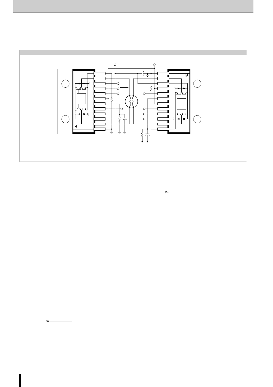
76
A3952SB/SLB/SW
2-Phase Stepper Motor Bipolar Driver ICs (2-Phase/1-2 Phase Excitation)
A3952SB/SLB/SW
I
LOAD
R
LOAD
(V
BEMF
+ V
BB
)
I
LOAD
V
REF
(10
•
R
S
)
R
T
•
C
T
(Chopping off-time setting)
12k~100k
Ω
820~1500pF (When using slow current-decay mode only)
1200~1500pF (When using fast current-decay mode only)
t
off
≅
R
T =
C
T =
PHASE
1
PHASE
2
MODE
1
MODE
2
V
REF1
V
REF2
ENABLE
1
ENABLE
2
10
9
8
7
6
5
4
1
3
2
12
11
LOGIC
LOGIC
V
BB
V
BB
V
BB
V
CC
V
CC
10
9
8
7
6
5
4
13
21
2
11
0.5
Ω
R
T=
17k
Ω/
25k
Ω
R
T=
17k
Ω/
25
k
Ω
C
T=
820pF/1200pF
C
T=
0.5
Ω
+5V
47 F
+
820pF/1200pF
µ
Fig. 4 Example of stepper motor drive
(F) Application circuit (Bipolar stepper motor drive)
(G)DC Motor Applications
In closed-loop systems, the speed of a dc motor can be con-
trolled by PWM of the PHASE or ENABLE inputs, or by varying
the REF input voltage (V
REF
). In digital systems (microproces-
sor controlled), PWM of the PHASE or ENABLE input is used
typically thus avoiding the need to generate a variable analog
voltage reference. In this case, a dc voltage on the REF input is
used typically to limit the maximum load current.
In dc servo applications that require accurate positioning at low
or zero speed, PWM of the PHASE input is selected typically.
This simplifies the servo-control loop because the transfer func-
tion between the duty cycle on the PHASE input and the aver-
age voltage applied to the motor is more linear than in the case
of ENABLE PWM control (which produces a discontinuous cur-
rent at low-current levels).
With bidirectional dc servo motors, the PHASE terminal can be
used for mechanical direction control. Similar to when braking
the motor dynamically, abrupt changes in the direction of a ro-
tating motor produce a currrent generated by the back EMF.
The current generated will depend on the mode of operation. If
the internal current-control circuitry is not being used, then the
maximum load current generated can be approximated by
where V
BEMF
is proportional to the motor’s speed. If the internal
slow-decay current-control circuitry is used, then the maximum
load current generated can be approximated by I
LOAD
=V
BEMF
/
R
LOAD
. For both cases, care must be taken to ensure the maxi-
mum ratings of the device are not exceeded. If the internal fast-
decay current-control circuitry is used, then the load current will
regulate to a value given by
CAUTION: In fast-decay mode, when the direction of the motor
is changed abruptly, the kinetic energy stored in the motor and
load inertia will be converted into current that charges the V
BB
supply bulk capacitance (power supply output and decoupling
capacitance). Care must be taken to ensure the capacitance is
sufficient to absorb the energy without exceeding the voltage
rating of any devices connected to the motor supply.
See also, the sections on brake operation under “Functional
Description,” above.
ac/Allegro/Allegro_Motor_Drive_ICs-html.html

77
A3952SB/SLB/SW
2-Phase Stepper Motor Bipolar Driver ICs (2-Phase/1-2 Phase Excitation)
A3952SB/SLB/SW
R
T
•
C
T
(Chopping off-time setting)
12k to 100k
Ω
820 to 1500pF (When using slow current-decay mode only)
1200 to 1500pF (When using fast current-decay mode only)
toff
≅
R
T
=
C
T
=
47 F
+
1
V
BB
V
BB
V
CC
V
BB
LOGIC
0.5
Ω
MODE
PHASE
ENABLE
BRAKE
+5 V
9
2
3
4
5
6
7
8
15
16
12
13
14
10
11
R
T=
17k
Ω/
25k
Ω
C
T=
820pF/1200pF
µ
(H) Application circuit (DC motor drive)
Fig. 5 Example of DC motor drive
ac/Allegro/Allegro_Motor_Drive_ICs-html.html
78
UDN2916B/LB
2-Phase Stepper Motor Bipolar Driver ICs
UDN2916B/LB
Allegro MicroSystems product
■
Features
●
Fixed off-time PWM current control
●
Internal 1/3 and 2/3 reference divider
●
1-phase/2-phase/W1-2 phase excitation
mode with digital input
●
Microstepping with reference input
●
Low saturation voltage (Sink transistor)
●
Internal thermal shutdown circuitry
●
Internal crossover-current protection cir-
cuitry
●
Internal UVLO protection
●
Internal transient-suppression diodes
●
Low thermal resistance package
■
Absolute Maximum Ratings
Parameter
Symbol
Conditions
Ratings
Units
UDN2916B
UDN2916LB
Motor supply voltage
V
BB
45
V
Output current (peak)
I
O (peak)
tw
≤
20
µ
s
±
1.0
A
Output current (continuous)
I
O
±
0.75
A
Logic supply voltage
V
CC
7.0
V
Logic input voltage range
V
IN
−
0.3 to +7.0
V
Output emitter voltage
V
E
1.5
V
Package power dissipation
P
D
(Note1)
3.12
2.27
W
Operating temperature
T
a
−
20 to +85
°
C
Junction temperature
T
j
(Note2)
+150
°
C
Storage temperature
T
stg
−
55 to +150
°
C
●
Output current rating may be limited by duty cycle, ambient temperature, and heat sinking. Under any
set of conditions, do not exceed the specified current rating or a junction temperature of 150
°
C.
Note 1: When ambient temperature is 25
°
C or over, derate using
−
25mW/
°
C (UDN2916B) or
−
18.2mW/
°
C (UDN2916LB).
Note 2: Fault conditions where junction temperature (T
j
) exceeds 150
°
C will activate the device’s thermal
shutdown circuitry. These conditions can be tolerated but should be avoided.
■
Electrical Characteristics
Parameter
Symbol
Conditions
Limits
Units
min
typ
max
Power outputs (OUT
A
or OUT
B
)
Motor supply voltage range
V
BB
10
45
V
Output leakage current
I
CEX
Sink driver, V
O
=V
BB
<1.0
50
µ
A
Source driver, V
O
=0V
<
−
1.0
−
50
µ
A
Output sustaining voltage
V
CE (SUS)
I
O
=
±
750mA, L=3.0mH
45
V
Sink driver, I
O
=+500mA
0.4
0.6
V
Output saturation voltage
V
CE (SAT)
Sink driver, I
O
=+750mA
1.0
1.2
V
Source driver, I
O
=
−
500mA
1.0
1.2
V
Source driver, I
O
=
−
750mA
1.3
1.5
V
Clamp diode leakage current
I
R
V
R
=45V
<1.0
50
µ
A
Clamp diode forward voltage
V
F
I
F
=750mA
1.6
2.0
V
Motor supply current
I
BB (ON)
Both bridges ON, no load
20
25
mA
I
BB (OFF)
Both bridges OFF
5.0
10
mA
Control logic
Input voltage
V
IH
All inputs
2.4
V
V
IL
All inputs
0.8
V
Input current
I
IH
V
IH
=2.4V
<1.0
20
µ
A
I
IL
V
IL
=0.8V
−
3.0
−
200
µ
A
Reference voltage range
V
REF
Operating
1.5
7.5
V
I
0
=I
1
=0.8V
9.5
10.0
10.5
Current control threshold
V
REF
/V
SENSE
I
0
=2.4V, I
1
=0.8V
13.5
15.0
16.5
I
0
=0.8V, I
1
=2.4V
25.5
30.0
34.5
Thermal shutdown temperature
T
j
170
°
C
Logic supply current
I
CC (ON)
I
0
=I
1
=0.8V, no load
40
50
mA
I
CC (OFF)
I
0
=I
1
=2.4V, no load
10
12
mA
●
“typ” values are for reference.
(Unless specified otherwise, T
a
=25
°
C, V
BB
=45V, V
CC
=4.75V to 5.25V, V
REF
=5.0V)
■
Terminal Connection Diagram
UDN2916B
OUT
1A
OUT
2A
V
BB
LOAD SUPPLY
E
1
SENSE
1
OUT
1B
I
01
I
11
PHASE
1
V
REF1
RC
1
LOGIC SUPPLY
GROUND
GROUND
OUT
2B
I
02
I
12
PHASE
2
V
REF2
RC
2
V
CC
2
1
GROUND
GROUND
PWM 2
PWM 1
E
2
SENSE
2
2
1
1
2
3
4
5
6
7
8
9
10
11
12
13
14
15
16
17
18
19
20
21
22
23
24
UDN2916LB
PHASE
2
V
REF 2
RC
2
RC
1
V
CC
V
BB
I
11
PHASE
1
V
REF1
GROUND
GROUND
LOGIC SUPPLY
I
12
I
02
2
24
23
22
21
20
19
18
17
16
15
14
13
3
4
5
6
7
8
9
10
11
12
1
1
2
2
1
PWM 1
PWM 2
LOAD SUPPLY
OUT
2B
OUT
2A
OUT
1B
OUT
1A
GROUND
GROUND
SENSE
2
SENSE
1
E
2
I
01
E
1
θ
θ
θ
θ
2-Phase/1-2 Phase/W1-2 Phase Excitation
ac/Allegro/Allegro_Motor_Drive_ICs-html.html
79
UDN2916B/LB
2-Phase Stepper Motor Bipolar Driver ICs (2-Phase/1-2 Phase/W1-2 Phase Excitation)
UDN2916B/LB
■
Internal Block Diagram
(1/2 Circuit)
■
Derating
■
Truth Table
■
External Dimensions
■
Application Circuit
(UDN2916LB)
Plastic DIP (300mil)
Wide body plastic SOP (300mil)
PHASE
OUT
A
OUT
B
H
L
H
L
L
H
I
0
I
1
Output Current
L
H
L
H
L
L
H
H
V
REF
/ (
10
×
R
S
)=
I
TRIP
V
REF
/ (
15
×
R
S
)=
I
TRIP
×
2/3
V
REF
/ (
30
×
R
S
)=
I
TRIP
×
1/3
0
V
REF
R
S
R
C
RC
SOURCE
DISABLE
R
T
C
T
C
C
I
0
I
1
E
SENSE
20 k
Ω
40 k
Ω
10 k
Ω
OUT
A
OUT
B
V
BB
÷
10
ONE
SHOT
−
+
UDN2916B
UDN2916LB
4
5
3
2
1
0
−
20
0
25
50
75
100
85
UDN2916B 40
°
C/
W
UDN2916LB 55
°
C/ W
Ambient temperature Ta (
°
C)
Allowable package power dissipation P
D
(W)
1.27
0.40
0.32
0.23
10.65
10.00
7.60
7.40
15.60
15.20
0.51
0.33
1
2
3
12
13
24
2.65
2.35
SEATING PLANE
0.10 MIN
1.27
BSC
0
°
TO 8
°
1.77
1
2
3
12
13
24
1.15
32.30
28.60
0.558
0.356
4.06
2.93
7.11
6.10
INDEX AREA
0.127MIN
7.62BSC
2.54BSC
5.33MAX
SEATING PLANE
0.39MIN
0.381
0.204
●
Thickness of lead is measured below seating plane.
●
Allowable variation in distance between leads is not cumulative.
V
CC
V
BB
V
BB
C
BB
2
24
23
22
21
20
19
18
17
16
15
14
13
3
4
5
6
7
8
9
10
11
12
1
1
2
1
PWM 1
PWM 2
2
*1
*1
*1
*1
*1
*1
*2
*1
From P
*2 V
REF
*2
C
T
C
T
C
C
C
C
V
CC
R
T
R
T
R
C
R
C
R
S
R
S
M
+5V
●
Off-time setting
t
off
≅
C
T
R
T
(Unit: mm)
R
S
: 1.5
Ω
, 1/2W (1.0 to 2.0
Ω
, 1 to 1/2W)
V
REF
: 5.0V (1.5 to 7.5V)
R
T
: 56k
Ω
(20k to 100k
Ω
)
C
T
: 470pF (100 to 1,000pF)
R
C
: 1k
Ω
C
C
: 4,700pF (470 to 10,000pF)
C
BB
: 100 F
ICs per stick
15
ICs per stick
31
●
Pin material: copper, pin surface treatment: solder plating
●
Package index may be *1.
●
Allowable variation in distance between leads is not cumulative.
●
Web (batwing) type lead frames are used for pin 6, 7, 18, 19.
The pins are connected to GND.
*1
µ
µ
θ
θ
ac/Allegro/Allegro_Motor_Drive_ICs-html.html
80
UDN2916B/LB
2-Phase Stepper Motor Bipolar Driver ICs (2-Phase/1-2 Phase/W1-2 Phase Excitation)
UDN2916B/LB
●
PWM CURRENT CONTROL
The UDN2916B/LB dual bridges are designed to drive both wind-
ings of a bipolar stepper motor. Output current is sensed and
controlled independently in each bridge by an external sense
resistor (R
S
), internal comparator, and monostable multivibrator.
When the bridge is turned ON, current increases in the motor
winding and it is sensed by the external sense resistor until the
sense voltage (V
SENSE
) reaches the level set at the comparator’s
input:
The comparator then triggers the monostable which turns OFF
the source driver of the bridge. The actual load current peak
will be slightly higher than the trip point (especially for low-in-
ductance loads) because of the internal logic and switching de-
lays. This delay (t
d
) is typically 2
µ
s. After turn-off, the motor
current decays, circulating through the ground-clamp diode and
sink transistor. The source driver’s OFF time (and therefore the
magnitude of the current decrease) is determined by the
monostable’s external RC timing components, where t
off
=R
T
C
T
wihtin the range of 20k
Ω
to 100k
Ω
and 100pF to 1000 pF.
When the source driver is re-enabled, the winding current (the
sense voltage) is again allowed to rise to the comparator ’s
threshold. This cycle repeats itself, maintaining the average
motor winding current at the desired level.
Loads with high distributed capacitances may result in high turn-
ON current peaks. This peak (appearing across R
S
) will attempt
to trip the comparator, resulting in erroneous current control or
high-frequency oscillations. An external R
C
C
C
time delay should
be used to further delay the action of the comparator. Depend-
ing on load type, many applications will not require these exter-
nal components (SENSE connected to E.)
V
PHASE
I
OUT
I
TRIP
t
d
t
off
+
−
0
I
TRIP
=V
REF
/ 10R
S
V
BB
R
SENSE
Load
BRIDGE ON
SOURCE OFF
ALL OFF
PWM OUTPUT CURRENT WAVE FORM
Load-Current Paths
Application Notes
●
LOGIC CONTROL OF OUTPUT CURRENT
Two logic level inptus (I
0
and I
1
) allow digital selection of the
motor winding current at 100%, 67%, 33%, or 0% of the maxi-
mum level per the table. The 0% output current condition turns
OFF all drivers in the bridge and can be used as an OUTPUT
ENABLE function.
These logic level inputs greatly enhance the implementation of
µ
P-controlled drive formats.
During half-step operations, the I
0
and I
1
allow the
µ
P to control
the motor at a constant torque between all positions in an eight-
step sequence. This is accomplished by digitally selecting 100%
drive current when only one phase is ON and 67% drive current
when two phases are ON. Logic highs on both I
0
and I
1
turn
OFF all drivers to allow rapid current decay when switching
phases. This helps to ensure proper motor operation at high
step rates.
The logic control inputs can also be used to select a reduced
current level (and reduced power dissipation) for ‘hold’ condi-
tions and/or increased current (and available torque) for start-
up conditions.
●
SWITCHING THE EXCITATION CURRENT DIRECTION
The PHASE input to each bridge determines the direction moter
winding current flows. An internally generated deadtime (ap-
proximately 2
µ
s) prevents crossover currents that can occur
when switching the PHASE input.
ac/Allegro/Allegro_Motor_Drive_ICs-html.html
81
UDN2916B/LB
2-Phase Stepper Motor Bipolar Driver ICs (2-Phase/1-2 Phase/W1-2 Phase Excitation)
UDN2916B/LB
●
REDUCTION AND DISPERSION OF POWER LOSS
The thermal performance can be improved by adding four ex-
ternal Schottky barrier diodes (AK03 or other) between each
output terminal and ground. In most applications, the chopping
ON time is shorter than the chopping OFF time (small ON duty).
Therefore, a great part of the power loss of the driver IC is at-
tributable to the motor regenerative current during the chopping
OFF period. The regenerative current from the motor flows
through the current sensing resistor and ground clamp diode
and returns to the motor. The voltage drop across this path
causes the power loss. On this path, the forward voltage VF of
ground clamp diode shows the greatest drop. This means that
adding Schottky barrier diodes will improve the thermal perfor-
mance if their V
F
characteristic is smaller than that of the inter-
nal ground clamp diode.
The external diodes also disperse the loss (a source of heat)
and reduce the package power dissipation P
D
of the driver IC.
Consequently, a greater output current can be obtained.
●
CONTROL SEQUENCE OF 1-2 OR W1-2 PHASE EXCITATION
To reduce vibration when the stepper motor is rotating, the
UDN2916B/LB can provide 1-2 or W1-2 phase excitation for
the control sequence without varying the V
REF
terminal voltage.
The step angle is
OUT
1A
OUT
1B
OUT
2A
OUT
2B
GND
Schottky barrier
diode
To motor
Note: When the sequence no. is 0, 4, 8, or 12, power-down can be set as follows
I
11
=1, I
01
=0: Sequence No. 0 or 8
I
12
=1, I
02
=0: Sequence No. 4 or 12
If power-down is necessary for a sequence other than 0, 4, 8, or 12, lower the V
REF
terminal voltage. However, do not set the voltage lower than the lower limit of the setting range.
(NABLE1= ENABLE 2= 0)
Phase A
Sequence
No.
I
11
I
01
Current ratio
PH
1
Phase B
I
12
I
02
Current ratio
PH
2
0
0
0
0
1
X
1
1
0
*
*
1
0
0
0
1
0
1
0
1/3
*
2
0
0
1
2/3
0
0
1
2/3
*
*
3
0
1
0
1/3
0
0
0
1
*
4
X
1
1
0
0
0
0
1
*
*
5
1
1
0
1/3
0
0
0
1
*
6
1
0
1
2/3
0
0
1
2/3
*
*
7
1
0
0
1
0
1
0
1/3
*
8
1
0
0
1
X
1
1
0
*
*
9
1
0
0
1
1
1
0
1/3
*
10
1
0
1
2/3
1
0
1
2/3
*
*
11
1
1
0
1/3
1
0
0
1
*
12
X
1
1
0
1
0
0
1
*
*
13
0
1
0
1/3
1
0
0
1
*
14
0
0
1
2/3
1
0
1
2/3
*
*
15
0
0
0
0
1
1
0
1/3
*
1-2 phase
excitation
W1-2 phase
excitation
Phase B
Phase A
(4)
(3)
(2)
(1)
(0)
Combined vector (1/4 cycle)
Control sequence (1-2/W1-2 phase)
1/2 step : 1-2 excitation
About 1/4 step : W1-2 excitation
The control sequence is as shown below. (This sequence uses
threshold signal terminals Io and I
1
for PWM current control.)
ac/Allegro/Allegro_Motor_Drive_ICs-html.html
82
UDN2916B/LB
2-Phase Stepper Motor Bipolar Driver ICs (2-Phase/1-2 Phase/W1-2 Phase Excitation)
UDN2916B/LB
Note: The V
REF
terminal voltage cannot be set to 0 V. To make the output current ratio 0%, set I
0X
=I
1X
=1.
When the sequence is 0, 8, 16, or 24, power-down can be set as follows:
I
11
=1, I
01
=0: Sequence No. 0 or 16
I
12
=1, I
02
=0: Sequence No. 8 or 24
Phase A
Sequence
No.
I
11
I
01
Current ratio (%)
PH
1
V
REF1
(V)
I
12
I
02
Current ratio (%)
PH
2
V
REF2
(V)
Phase B
0
0
7.5
0
0
100
X
1.5
1
1
0
1
0
7.4
0
0
98
0
1.5
0
0
20
2
0
6.9
0
0
92
0
2.9
0
0
38
3
0
6.2
0
0
83
0
4.2
0
0
56
4
0
5.3
0
0
71
0
5.3
0
0
71
5
0
4.2
0
0
56
0
6.2
0
0
83
6
0
2.9
0
0
38
0
6.9
0
0
92
7
0
1.5
0
0
20
0
7.4
0
0
98
8
X
1.5
1
1
0
0
7.5
0
0
100
9
1
1.5
0
0
20
0
7.4
0
0
98
10
1
2.9
0
0
38
0
6.9
0
0
92
11
1
4.2
0
0
56
0
6.2
0
0
83
12
1
5.3
0
0
71
0
5.3
0
0
71
13
1
6.2
0
0
83
0
4.2
0
0
56
14
1
6.9
0
0
92
0
2.9
0
0
38
15
1
7.4
0
0
98
0
1.5
0
0
20
16
1
7.5
0
0
100
X
1.5
1
1
0
17
1
7.4
0
0
98
1
1.5
0
0
20
18
1
6.9
0
0
92
1
2.9
0
0
38
19
1
6.2
0
0
83
1
4.2
0
0
56
20
1
5.3
0
0
71
1
5.3
0
0
71
21
1
4.2
0
0
56
1
6.2
0
0
83
22
1
2.9
0
0
38
1
6.9
0
0
92
23
1
1.5
0
0
20
1
7.4
0
0
98
24
X
1.5
1
1
0
1
7.5
0
0
100
25
0
1.5
0
0
20
1
7.4
0
0
98
26
0
2.9
0
0
38
1
6.9
0
0
92
27
0
4.2
0
0
56
1
6.2
0
0
83
28
0
5.3
0
0
71
1
5.3
0
0
71
29
0
6.2
0
0
83
1
4.2
0
0
56
30
0
6.9
0
0
92
1
2.9
0
0
38
31
0
7.4
0
0
98
1
1.5
0
0
20
●
V
REF
terminal
V
REF
is the reference voltage input terminal for PWM constant
current control. To realize stable ensure a stable signal, make
sure noise is not applied to the terminal.
●
V
BB
terminal
To prevent voltage spikes on the load power supply terminal
(V
BB
), connect a large capacitor (
≥
22
µ
F) between the V
BB
termi-
nal and ground as close to the device as possible. Make sure
the load supply voltage does not exceed 45 V.
Control sequence (microstepping)
●
MICROSTEPPING (1/8 STEP) CONTROL SEQUENCE
Varying the V
REF
terminal voltage in steps provides 1/8
microstepping and reduces motor vibration greatly. The
microstepping control sequence is as follows:
●
Thermal protection
Thermal protection circuitry turns OFF all drivers when the junc-
tion temperature reaches +170
°
C. It is only intended to protect
the device from failures due to excessive junction temperature
and should not imply that output short circuits are permitted.
The output drivers are re-enabled when the junction tempera-
ture cools to +145
°
C.
ac/Allegro/Allegro_Motor_Drive_ICs-html.html
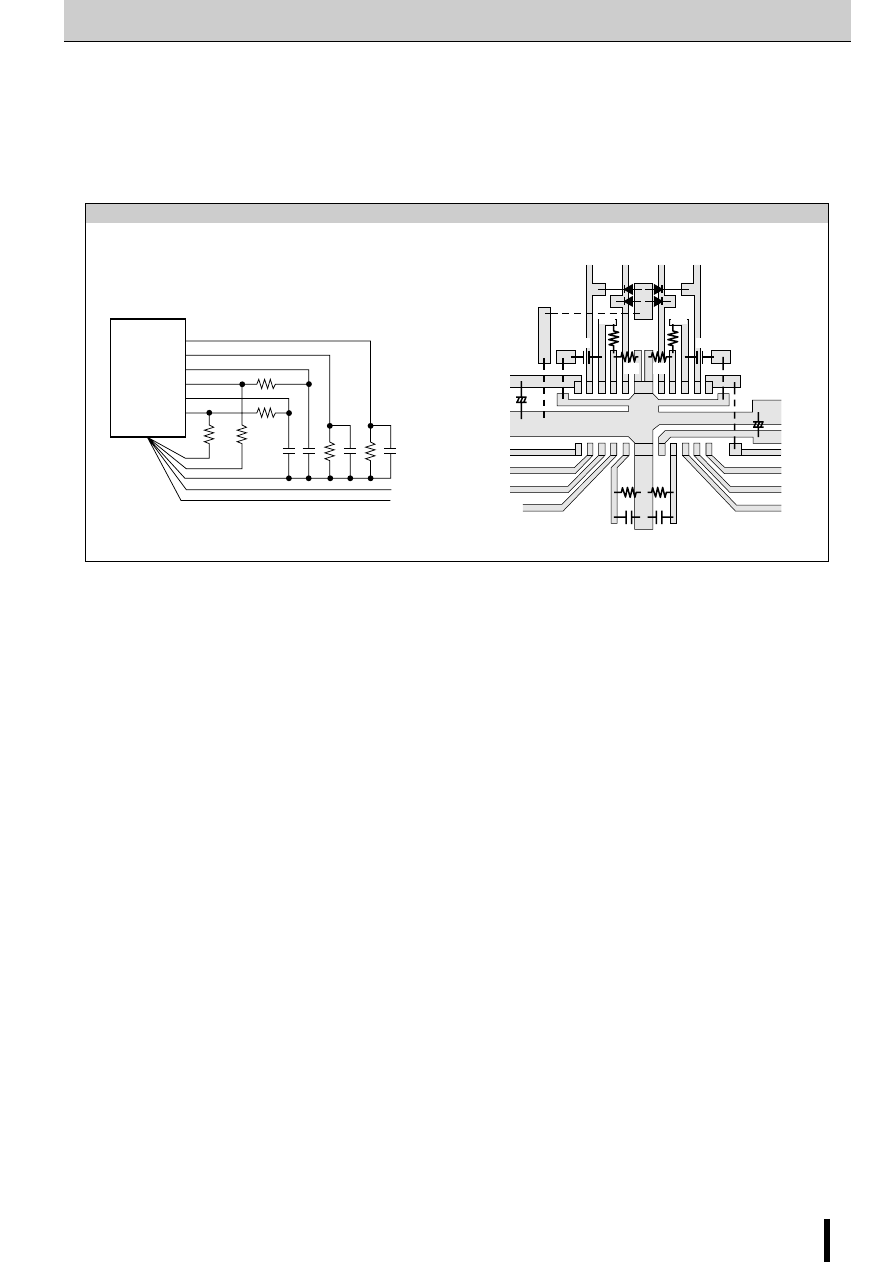
83
UDN2916B/LB
2-Phase Stepper Motor Bipolar Driver ICs (2-Phase/1-2 Phase/W1-2 Phase Excitation)
UDN2916B/LB
UDN2916B
UDN2916LB
R
S
R
S
R
C
R
T
R
T
C
C
V
BB
GND
V
CC
GND
C
C
C
T
C
T
R
C
6, 7,
18, 19
+
+
OUT
2B
R
T
C
T
V
BB
V
BB
I
02
I
12
Ph
2
V
REF2
V
REF1
GND
V
CC
V
CC
V
BB
I
01
I
11
Ph
1
GND
C
T
R
T
OUT
1B
OUT
2A
OUT
1A
R
C
R
S
R
S
R
C
C
C
C
C
●
Around the ground
Since the UDN2916B/LB is a chopping type power driver IC,
take great care around the ground when mounting. Separate
the power system and the small signal (analog) system. Pro-
vide a single-point connection to the GND terminal or a solid
pattern of low enough impedance.
Example of Circuit (including GND) and GND Wiring Pattern (UDN2916LB)
ac/Allegro/Allegro_Motor_Drive_ICs-html.html
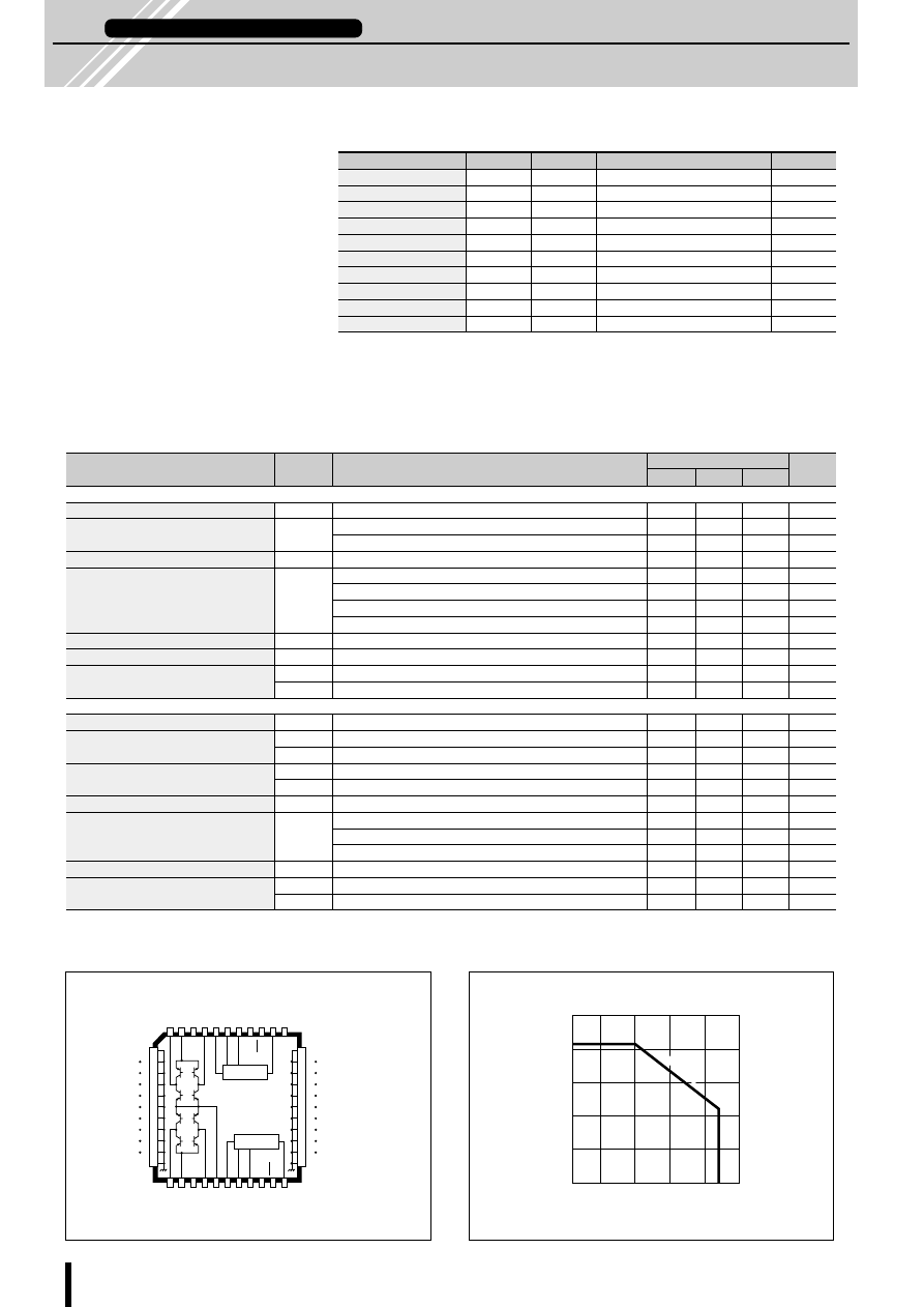
84
UDN2917EB
2-Phase Stepper Motor Bipolar Driver IC
UDN2917EB
Allegro MicroSystems product
■
Features
●
Fixed off-time PWM current control
●
Internal 1/3 and 2/3 reference divider
●
1-phase/2-phase/W1-2 phase excitation
mode with digital input
●
Microstepping with reference input
●
Low saturation voltage (Sink transistor)
●
Internal thermal shutdown circuitry
●
Internal crossover-current protection cir-
cuitry
●
Internal UVLO protection
●
Internal transient-suppression diodes
●
Low thermal resistance 44-pin PLCC
■
Absolute Maximum Ratings
Parameter
Symbol
Conditions
Ratings
Units
Motor supply voltage
V
BB
45
V
Output current (peak)
I
O (peak)
tw
≤
20
µ
s
±
1.75
A
Output current (continuous)
I
O
±
1.5
A
Logic supply voltage
V
CC
7.0
V
Logic input voltage range
V
IN
−
0.3 to +7.0
V
Output emitter voltage
V
E
1.0
V
Package power dissipation
P
D
(Note1)
4.16
W
Operating temperature
T
a
−
20 to +85
°
C
Junction temperature
T
j
(Note2)
+150
°
C
Storage temperature
T
stg
−
55 to +150
°
C
●
Output current rating may be limited by duty cycle, ambient temperature, and heat sinking. Under any
set of conditions, do not exceed the specified current rating or a junction temperature of 150
°
C.
Note 1: When ambient temperature is 25
°
C or over, derate using
−
33.3mW/
°
C.
Note 2: Fault conditions where junction temperature (T
j
) exceeds 150
°
C will activate the device’s thermal
shutdown circuitry. These conditions can be tolerated but should be avoided.
■
Electrical Characteristics
Parameter
Symbol
Conditions
Limits
Units
min
typ
max
Power outputs (OUT
A
or OUT
B
)
Motor supply voltage range
V
BB
10
45
V
Output leakage current
I
CEX
Sink driver, V
O
=V
BB
<1.0
50
µ
A
Source driver, V
O
=0V
<
−
1.0
−
50
µ
A
Output sustaining voltage
V
CE (SUS)
I
O
=
±
1.5A, L=3.5mH
45
V
Sink driver, I
O
=+1.0A
0.5
0.7
V
Output saturation voltage
V
CE (SAT)
Sink driver, I
O
=+1.5A
0.8
1.0
V
Source driver, I
O
=
−
1.0A
1.8
1.9
V
Source driver, I
O
=
−
1.5A
1.9
2.1
V
Clamp diode leakage current
I
R
V
R
=45V
<1.0
50
µ
A
Clamp diode forward voltage
V
F
I
F
=1.5A
1.6
2.0
V
Motor supply current
I
BB (ON)
Both bridges ON, no load
9.0
12
mA
I
BB (OFF)
Both bridges OFF
4.0
6.0
mA
Control logic
Logic supply voltage
V
CC
Operating
4.75
5.0
5.25
V
Input voltage
V
IH
All inputs
2.4
V
V
IL
All inputs
0.8
V
Input current
I
IH
V
IH
=2.4V
<1.0
20
µ
A
I
IL
V
IL
=0.8V
−
3.0
−
200
µ
A
Reference voltage range
V
REF
Operating
1.5
7.5
V
I
0
=I
1
=0.8V
9.5
10.0
10.5
Current control threshold
V
REF
/V
SENSE
I
0
=2.4V, I
1
=0.8V
13.5
15.0
16.5
I
0
=0.8V, I
1
=2.4V
25.5
30.0
34.5
Thermal shutdown temperature
T
j
170
°
C
Logic supply current
I
CC (ON)
I
0
=I
1
=V
EN
=0.8V, no load
90
105
mA
I
CC (OFF)
I
0
=I
1
=2.4V, no load
10
12
mA
●
“typ” values are for reference.
(Unless specified otherwise, T
a
=25
°
C, V
BB
=45V, V
CC
=5.0V, V
REF
=5.0V)
■
Terminal Connection Diagram
GROUND
GROUND
GROUND
GROUND
8
9
10
11
12
13
14
15
16
17
39
38
37
36
35
34
33
32
31
30
29
7
OUT
1A
OUT
1B
I
10
I
11
V
REF1
V
CC
V
BB
E
1
SENSE
1
PHASE
1
RC
1
1
EN
1
LOGIC SUPPLY
ENABLE
1
OUT
2A
OUT
2B
I
20
I
21
V
REF2
E
2
SENSE
2
PHASE
2
RC
2
LOAD SUPPLY
ENABLE
2
6
5
4
3
2
1
44
43
42
41
40
2
EN
2
PWM 1
PWM 2
18
19
20
21
22
23
24
25
26
27
28
1
2
■
Derating
4
5
3
2
1
0
−
20
0
25
50
75
100
85
Ambient temperature Ta (
°
C)
Allowable package power dissipation
P
D
(W)
30
°
C/
W
θ
θ
2-Phase/1-2 Phase/W1-2 Phase Excitation
ac/Allegro/Allegro_Motor_Drive_ICs-html.html
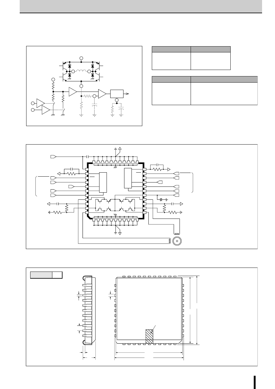
85
UDN2917EB
2-Phase Stepper Motor Bipolar Driver IC (2-Phase/1-2 Phase/W1-2 Phase Excitation)
UDN2917EB
■
Truth Table
■
External Dimensions
Plastic PLCC
■
Application Circuit
(Unit: mm)
PWM 1
PWM 2
1
2
V
BB
V
BB
STEPPER
MOTOR
V
CC
V
CC
C
t
C
t
R
t
R
t
EN
1
1
2
EN
2
ENABLE
1
Digital control signal
Digital control signal
PHASE
1
ENABLE
2
PHASE
2
V
REF1
V
REF2
I
11
C
C
C
C
C
VBB
R
S
R
S
R
C
R
C
I
01
I
12
I
02
+
28
27
26
25
24
23
22
21
20
19
18
17
16
15
14
13
12
11
10
9
8
7
6
5
4
3
2
1
44
43
42
41
40
39
38
37
36
35
34
33
32
31
30
29
●
Off-time setting
t
off
≅
C
T
R
T
R
S
: 0.82
Ω
, 1W (0.5 to 1.0
Ω
, 2 to 1W)
V
REF
: 5.0V (1.5 to 7.5V)
R
T
: 56k
Ω
(20k to 100k
Ω
)
C
T
: 470pF (200 to 500pF)
R
C
: 1k
Ω
C
C
: 3,300pF (470 to 10,000pF)
C
VBB
: 100 F
0.51
MIN
4.57
4.19
0.533
0.331
16.66
16.51
16.66
16.51
17.65
17.40
17.65
17.40
1.27
BSC
44
1
2
INDEX AREA
0.812
0.661
ENABLE
PHASE
OUT
A
OUT
B
L
L
H
H
L
X
H
L
Z
L
H
Z
X=Don't Care Z=High impedance
I
0
I
1
Output Current
L
H
L
H
L
L
H
H
V
REF
/
(10
×
R
S
)=I
TRIP
V
REF
/
(15
×
R
S
)=I
TRIP
×
2/3
V
REF
/
(30
×
R
S
)=I
TRIP
×
1/3
0
●
Allowable variation in distance between leads is not cumulative.
Note 1: Web type leads are internally connected together.
ICs per stick
27
■
Internal Block Diagram
(1/2 Circuit)
V
REF
R
S
R
C
RC
SOURCE
DISABLE
R
T
C
T
C
C
I
0
I
1
E
SENSE
20 k
Ω
40 k
Ω
10 k
Ω
OUT
A
OUT
B
V
BB
÷
10
ONE
SHOT
−
+
θ
θ
µ
ac/Allegro/Allegro_Motor_Drive_ICs-html.html
86
UDN2917EB
2-Phase Stepper Motor Bipolar Driver IC (2-Phase/1-2 Phase/W1-2 Phase Excitation)
UDN2917EB
Note: When the sequence no. is 0, 4, 8, or 12, power-down can be set as follows
I
11
=1, I
01
=0: Sequence No. 0 or 8
I
12
=1, I
02
=0: Sequence No. 4 or 12
If power-down is necessary for a sequence other than 0, 4, 8, or 12, lower the
V
REF
terminal voltage. However, do not set the voltage lower than the lower limit of the setting range.
(ENABLE1= ENABLE 2=0)
Phase A
Sequence
No.
I
11
I
01
Current ratio
PH
1
Phase B
I
12
I
02
Current ratio
PH
2
0
0
0
0
1
X
1
1
0
*
*
1
0
0
0
1
0
1
0
1/3
*
2
0
0
1
2/3
0
0
1
2/3
*
*
3
0
1
0
1/3
0
0
0
1
*
4
X
1
1
0
0
0
0
1
*
*
5
1
1
0
1/3
0
0
0
1
*
6
1
0
1
2/3
0
0
1
2/3
*
*
7
1
0
0
1
0
1
0
1/3
*
8
1
0
0
1
X
1
1
0
*
*
9
1
0
0
1
1
1
0
1/3
*
10
1
0
1
2/3
1
0
1
2/3
*
*
11
1
1
0
1/3
1
0
0
1
*
12
X
1
1
0
1
0
0
1
*
*
13
0
1
0
1/3
1
0
0
1
*
14
0
0
1
2/3
1
0
1
2/3
*
*
15
0
0
0
0
1
1
0
1/3
*
1-2 phase
excitation
W1-2 phase
excitation
Application Notes
●
REDUCTION AND DISPERSION OF POWER LOSS
The thermal performance can be improved by adding four ex-
ternal Schottky barrier diodes (EK13 or other) between each
output terminal and ground. In most applications, the chopping
ON time is shorter than the chopping OFF time (small ON duty).
Therefore, a great part of the power loss of the driver IC is at-
tributable to the motor regenerative current during the chopping
OFF period. The regenerative current from the motor flows
through the current sensing resistor and ground clamp diode
and returns to the motor. The voltage drop across this path
causes the power loss. On this path, the forward voltage V
F
of
ground clamp diode shows the greatest drop. This means that
adding Schottky barrier diodes will improve the thermal perfor-
mance if their V
F
characteristic is smaller than that of the inter-
nal ground clamp diode.
The external diodes also disperse the loss (a source of heat)
and reduce the package power dissipation P
D
of the driver IC.
Consequently, a greater output current can be obtained.
●
CONTROL SEQUENCE OF 1-2 OR W1-2 PHASE EXCITATION
To reduce vibration when the stepper motor is rotating, the
UDN2917EB can provide 1-2 or W1-2 phase excitation for the
control sequence without varying the V
REF
terminal voltage.
The step angle is
OUT
1A
OUT
1B
OUT
2A
OUT
2B
GND
Schottky barrier
diode
To motor
Combined vector (1/4 cycle)
Phase B
Phase A
(4)
(3)
(2)
(1)
(0)
Control sequence (1-2/W1-2 phase)
1/2 step : 1-2 excitation
About 1/4 step : W1-2 excitation
The control sequence is as shown below. (This sequence uses
threshold signal terminals Io and I
1
for PWM current control.)
ac/Allegro/Allegro_Motor_Drive_ICs-html.html
87
UDN2917EB
2-Phase Stepper Motor Bipolar Driver IC (2-Phase/1-2 Phase/W1-2 Phase Excitation)
UDN2917EB
Note: The V
REF
terminal voltage cannot be set to 0 V. To make the output current ratio 0%, set I
0X
=I
1X
=1.
When the sequence is 0, 8, 16, or 24, power-down can be set as follows:
I
11
=1, I
01
=0: Sequence No. 0 or 16
I
12
=1, I
02
=0: Sequence No. 8 or 24
(ENABLE1= ENABLE 2=0)
Phase A
Sequence
No.
I
11
I
01
Current ratio (%)
PH
1
V
REF1
(V)
I
12
I
02
Current ratio (%)
PH
2
V
REF2
(V)
Phase B
0
0
7.5
0
0
100
X
1.5
1
1
0
1
0
7.4
0
0
98
0
1.5
0
0
20
2
0
6.9
0
0
92
0
2.9
0
0
38
3
0
6.2
0
0
83
0
4.2
0
0
56
4
0
5.3
0
0
71
0
5.3
0
0
71
5
0
4.2
0
0
56
0
6.2
0
0
83
6
0
2.9
0
0
38
0
6.9
0
0
92
7
0
1.5
0
0
20
0
7.4
0
0
98
8
X
1.5
1
1
0
0
7.5
0
0
100
9
1
1.5
0
0
20
0
7.4
0
0
98
10
1
2.9
0
0
38
0
6.9
0
0
92
11
1
4.2
0
0
56
0
6.2
0
0
83
12
1
5.3
0
0
71
0
5.3
0
0
71
13
1
6.2
0
0
83
0
4.2
0
0
56
14
1
6.9
0
0
92
0
2.9
0
0
38
15
1
7.4
0
0
98
0
1.5
0
0
20
16
1
7.5
0
0
100
X
1.5
1
1
0
17
1
7.4
0
0
98
1
1.5
0
0
20
18
1
6.9
0
0
92
1
2.9
0
0
38
19
1
6.2
0
0
83
1
4.2
0
0
56
20
1
5.3
0
0
71
1
5.3
0
0
71
21
1
4.2
0
0
56
1
6.2
0
0
83
22
1
2.9
0
0
38
1
6.9
0
0
92
23
1
1.5
0
0
20
1
7.4
0
0
98
24
X
1.5
1
1
0
1
7.5
0
0
100
25
0
1.5
0
0
20
1
7.4
0
0
98
26
0
2.9
0
0
38
1
6.9
0
0
92
27
0
4.2
0
0
56
1
6.2
0
0
83
28
0
5.3
0
0
71
1
5.3
0
0
71
29
0
6.2
0
0
83
1
4.2
0
0
56
30
0
6.9
0
0
92
1
2.9
0
0
38
31
0
7.4
0
0
98
1
1.5
0
0
20
Control sequence (microstepping)
●
V
REF
terminal
V
REF
is the reference voltage input terminal for PWM constant
current control. To realize stable ensure a stable signal, make
sure noise is not applied to the terminal.
●
V
BB
terminal
To prevent voltage spikes on the load power supply terminal
(V
BB
), connect a large capacitor (
≥
47
µ
F) between the V
BB
termi-
nal and ground as close to the device as possible. Make sure
the load supply voltage does not exceed 45V.
●
MICROSTEPPING (1/8 STEP) CONTROL SEQUENCE
Varying the V
REF
terminal voltage in steps provides 1/8
microstepping and reduces motor vibration greatly. The
microstepping control sequence is as follows:
●
Thermal protection
Thermal protection circuitry turns OFF all drivers when the junc-
tion temperature reaches +170
°
C. It is only intended to protect
the device from failures due to excessive junction temperature
and should not imply that output short circuits are permitted.
The output drivers are re-enabled when the junction tempera-
ture cools to +145
°
C.
●
Around the ground
Since the UDN2917EB is a chopping type power driver IC, take
great care around the ground when mounting. Separate the
power system and the small signal (analog) system. Provide a
single-point connection to the GND terminal or a solid pattern of
low enough impedance.
ac/Allegro/Allegro_Motor_Drive_ICs-html.html
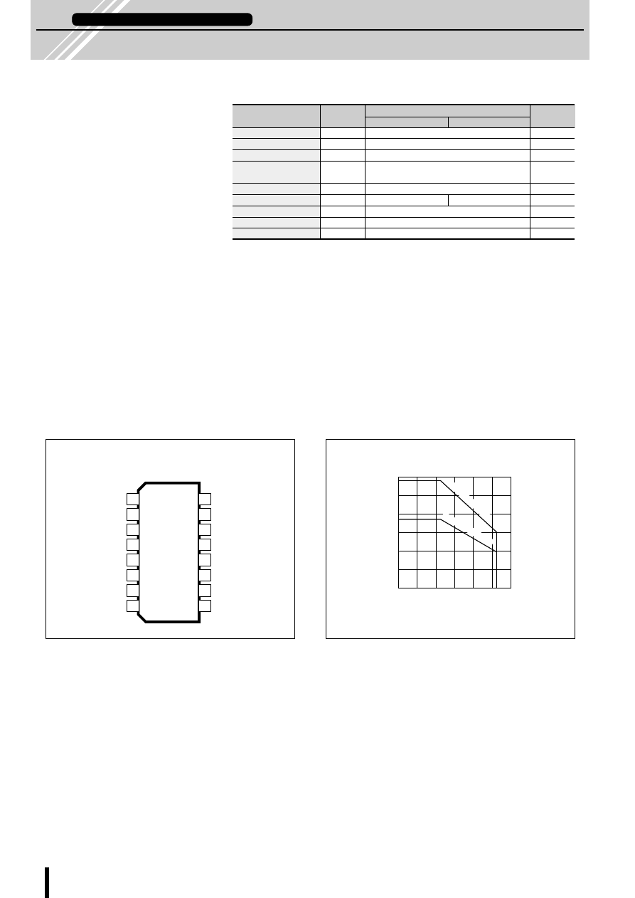
88
A3955SB/SLB
2-Phase Stepper Motor Bipolar Driver ICs
A3955SB/SLB
■
Features
●
Maximum output ratings: 50V,
±
1.5A
●
Internal 3-bit non-linear DAC for 8-division
microstepping enables 2W1-2,W1-2, 1-2,
2-phase excitation drive without external
sine wave generator
●
Internal PWM current control in Mixed De-
cay mode (can also be used in Fast Decay
and Slow Decay mode), which improves
motor current response and stability with-
out deterioration of motor iron loss
●
External RC filter for sense terminal not
required thanks to internal blanking circuitry
●
Internal thermal shutdown, crossover-cur-
rent protection and transient-suppression
diodes
●
Special power-up and power-down se-
quencing for motor supply and logic sup-
ply not required
●
Employs copper batwing lead frame with
low thermal resistance
■
Absolute Maximum Ratings
Parameter
Symbol
Ratings
Units
A3955SB
A3955SLB
Load supply voltage
V
BB
50
V
Output current (continuous)
I
O
±
1.5
A
Logic supply voltage
V
CC
7.0
V
Logic/reference input
V
IN
−
0.3 to V
CC
+0.3
V
voltage range
Sense voltage
V
S
1.0
V
Package power dissipation
P
D
(Note1)
2.90
1.86
W
Operating temperature
T
a
−
20 to +85
°
C
Junction temperature
T
j
(Note2)
+150
°
C
Storage temperature
T
stg
−
55 to +150
°
C
●
Output current rating may be limited by duty cycle, ambient temperature, and heat sinking. Under any
set of conditions, do not exceed the specified current rating or a junction temperature of 150
°
C.
Note 1: When ambient temperature is 25
°
C or over, derate using
−
23.26mW/
°
C(SB) or
−
14.93mW/
°
C(SLB).
Note 2: Fault conditions where junction temperature (T
j
) exceeds 150
°
C will activate the device’s thermal
shutdown circuitry. These conditions can be tolerated but should be avoided.
Allegro MicroSystems product
■
Terminal Connection Diagram
■
Derating
2
3
4
5
6
7
8
PFD
REF
RC
GROUND
GROUND
LOGIC
SUPPLY
PHASE
D
2
15
14
13
12
11
10
9
LOAD
SUPPLY
OUT
B
D
0
GROUND
GROUND
SENSE
OUT
A
D
1
(TOP VIEW)
1
16
3.0
2.5
2
Allo
w
a
b
le pac
kage po
w
e
r dissipation P
D
[W]
1.5
1
0.5
0
Ambient temperature Ta (
°
C)
−
20
0
20
40
60
80
100
A3955SLB 67
°
C/W
A3955SB 43
°
C/W
A3955SB/SLB
2W1-2 Phase Excitation/Micro-step Support
ac/Allegro/Allegro_Motor_Drive_ICs-html.html
89
A3955SB/SLB
2-Phase Stepper Motor Bipolar Driver ICs (2W1-2 Phase Excitation/Micro-step Support)
A3955SB/SLB
■
Electrical Characteristics
(Unless specified otherwise, T
a
=25
°
C, V
BB
=5V to 50V, V
CC
=4.5V to 5.5V)
Parameter
Symbol
Conditions
Limits
Units
min
typ
max
Power outputs (OUT
A
or OUT
B
)
Load supply voltage range
V
BB
Operating, I
O
=
±
1.5A, L=3mH
Vcc
50
V
Output leakage current
I
CEX
V
O
=V
BB
<1.0
50
µ
A
V
O
=0V
<
−
1.0
−
50
µ
A
V
SENSE
=1.0V : Source Driver, I
O
=
−
0.85A
1.0
1.2
V
Output saturation voltage
V
CE (sat)
V
SENSE
=1.0V : Source Driver, I
O
=
−
1.5A
1.3
1.5
V
V
SENSE
=1.0V : Sink Driver, I
O
=0.85A
0.5
0.6
V
V
SENSE
=1.0V : Sink Driver, I
O
=1.5A
1.3
1.5
V
Sense current offset
I
SO
I
S
-I
O
, I
O
=0.85A, V
S
=0V, V
CC
=5V
20
33
40
mA
Clamp diode forward voltage
V
F
I
F
=0.85A
1.2
1.4
V
I
F
=1.5A
1.4
1.7
V
Motor supply current (No load)
I
BB (ON)
2.0
4.0
mA
I
BB (OFF)
D
0
=D
1
=D
2
=0.8V
1.0
50
µ
A
Control logic
Logic supply voltage range
V
CC
Operating
4.5
5.0
5.5
V
Reference voltage range
V
REF
Operating
0.5
2.5
V
UVLO enable threshold
V
UVLOen
V
CC
=0
→
5V
3.35
3.70
4.05
V
UVLO hysteresis
V
UVLOhys
0.30
0.45
0.60
V
Logic supply current
I
CC (ON)
42
50
mA
I
CC (OFF)
D
0
=D
1
=D
2
=0.8V
12
16
mA
Logic input voltage
V
IH
2.0
V
V
IL
0.8
V
Logic input current
I
IH
V
IN
=2.0V
<1.0
20
µ
A
I
IL
V
IN
=0.8V
<
−
2.0
−
200
µ
A
Slow Decay Mode
3.5
V
Mixed Decay comparator trip points
V
PFD
Mixed Decay Mode
1.1
3.1
V
Fast Decay Mode
0.8
V
Mixed Decay comparator input offset voltage
V
IO (PFD)
0
±
20
mV
Mixed Decay compartor hysteresis
∆
V
IO (PFD)
5
25
55
mV
Reference input current
I
REF
V
REF
=0V~2.5V
±
5.0
µ
A
Reference divider ratio
V
REF
/V
S
at trip, D
0
=D
1
=D
2
=2V
3.0
DAC accuracy *1
DAC
ERR
V
REF
=1.0V~2.5V
±
3.0
%
V
REF
=0.5V~1.0V
±
4.0
%
Current-sense comparator input offset voltage *1
V
IO (S)
V
REF
=0V
±
5.0
mV
D
0
=D
1
=D
2
=0.8V
0
%
D
0
=2.0V, D
1
=D
2
=0.8V
19.5
%
D
0
=0.8V, D
1
=2V, D
2
=0.8V
38.2
%
Step reference current ratio
SRCR
D
0
=D
1
=2V, D
2
=0.8V
55.5
%
D
0
=D
1
=0.8V, D
2
=2V
70.7
%
D
0
=2V, D
1
=0.8V, D
2
=2V
83.1
%
D
0
=0.8V, D
1
=D
2
=2V
92.4
%
D
0
=D
1
=D
2
=2V
100
%
Thermal shutdown temperature
T
j
165
°
C
Thermal shutdown hysteresis
∆
T
j
15
°
C
AC timing
PWM RC fixed off-time
t
OFFRC
C
T
=470pF, R
T
=43k
Ω
18.2
20.2
22.3
µ
S
Current-Sense Comparator Trip to Source OFF,
PWM turn-off time
t
PWM (OFF)
I
O
=0.1A
1.0
1.5
µ
S
Current-Sense Comparator Trip to Source OFF,
I
O
=1.5A
1.4
2.5
µ
S
PWM turn-on time
t
PWM (ON)
I
RC
Charge ON to Source ON, I
O
=0.1A
0.4
0.7
µ
S
I
RC
Charge ON to Source ON, I
O
=1.5A
0.55
0.85
µ
S
PWM minimum on-time
t
ON (min)
V
CC
=5.0V, R
T
≥
43k
Ω
, C
T
=470pF,
1.0
1.6
2.2
µ
S
I
O
=0.1A
Crossover dead time
t
CODT
1k
Ω
Load to 25V
0.3
1.5
3.0
µ
S
*1: The total error for the V
REF
/V
SENSE
function is the sum of the D/A error and the current-sense comparator input offset voltage.
●
“typ” values are for reference.
ac/Allegro/Allegro_Motor_Drive_ICs-html.html
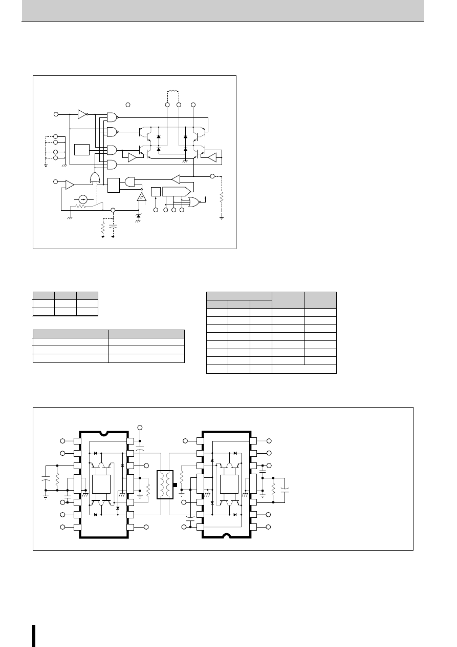
90
A3955SB/SLB
2-Phase Stepper Motor Bipolar Driver ICs (2W1-2 Phase Excitation/Micro-step Support)
A3955SB/SLB
■
Truth Table
■
Application Circuit
●
Off-time setting : t
OFF
≅
R
T
•
C
T
R
T
=12k
Ω
to 100k
Ω
C
T
=470pF to 1500pF
R
S
=0.39
Ω
to 0.62
Ω
C
BB
=47
µ
F+0.1
µ
F
C
CC
=0.1
µ
F
V
REF
=0.5V to 2.5V
V
PFD
=1.1V to 3.1V (Mixed current-decay mode)
≥
3.5V (Slow current-decay mode)
≤
0.8V (Fast current-decay mode)
BRIDGE A
V
BB
V
BB
V
CC
1
V
PFD
2
V
REF
3
R
T1
36 k
Ω
36 k
Ω
560 pF
560 pF
C
T1
6
+5V
7
PHASE
A
8
D
2A
C
CC1
5
4
16
15
14
11
10
9
D
1A
D
0B
D
1B
R
S1
C
BB1
D
0A
+
+
47 F
47 F
12
13
LOGIC
0.5
Ω
0.5
Ω
BRIDGE B
V
CC
9
10
11
R
S2
14
15
16
V
BB
C
BB2
13
12
8
7
6
3
2
1
V
PFD
V
REF
V
BB
PHASE
B
D
2B
R
T2
C
CC2
C
T2
+5 V
4
5
LOGIC
µ
µ
DAC
DAC DATA
DAC [%]
V
REF
/V
S
D
2
D
1
D
0
H
H
H
100
3.00
H
H
L
92.4
3.25
H
L
H
83.1
3.61
H
L
L
70.7
4.24
L
H
H
55.5
5.41
L
H
L
38.2
7.85
L
L
H
19.5
15.38
L
L
L
All Outputs Disabled
where V
S
≅
I
TRIP
*R
S
PHASE
PHASE
OUT
A
OUT
B
H
H
L
L
L
H
PFD
V
PFD
Operating Mode
≥
3.5V
Slow current-decay mode
1.1V to 3.1V
Mixed current-decay mode
≤
0.8V
Fast current-decay mode
■
Internal Block Diagram
PHASE
RC
3
7
Q
R
+3
D/A
+
−
+
−
+
−
S
BLANKING
GATE
PWM LATCH
CURRENT-SENSE
COMPARATOR
MIXED-DECAY
COMPARATOR
PFD
SENSE
DISABLE
BLANKING
R
T
C
T
V
TH
R
S
UVLO
& TSD
LOGIC
SUPPL
Y
LO
AD
SUPPL
Y
OUT
A
REF
D
2
D
1
D
0
OUT
B
V
CC
V
CC
V
BB
GROUND
4
5
12
13
1
11
16
15
10
6
2
8
9
14
ac/Allegro/Allegro_Motor_Drive_ICs-html.html
91
A3955SB/SLB
2-Phase Stepper Motor Bipolar Driver ICs (2W1-2 Phase Excitation/Micro-step Support)
A3955SB/SLB
■
Step Sequence
■
Current Vector Locus
Bridge A
Bridge B
Full
Half
Quarter
Eigth
Step
Step
Step
Step
PHASE
A
D
2A
D
1A
D
0A
I
LOADA
PHASE
B
D
2B
D
1B
D
0B
I
LOADB
1
1
1
1
H
H
L
L
70.7%
H
H
L
L
70.7%
2
H
L
H
H
55.5%
H
H
L
H
83.1%
2
3
H
L
H
L
38.2%
H
H
H
L
92.4%
4
H
L
L
H
19.5%
H
H
H
H
100%
2
3
5
X
L
L
L
0%
H
H
H
H
100%
6
L
L
L
H
−
19.5%
H
H
H
H
100%
4
7
L
L
H
L
−
38.2%
H
H
H
L
92.4%
8
L
L
H
H
−
55.5%
H
H
L
H
83.1%
2
3
5
9
L
H
L
L
−
70.7%
H
H
L
L
70.7%
10
L
H
L
H
−
83.1%
H
L
H
H
55.5%
6
11
L
H
H
L
−
92.4%
H
L
H
L
38.2%
12
L
H
H
H
−
100%
H
L
L
H
19.5%
4
7
13
L
H
H
H
−
100%
X
L
L
L
0%
14
L
H
H
H
−
100%
L
L
L
H
−
19.5%
8
15
L
H
H
L
−
92.4%
L
L
H
L
−
38.2%
16
L
H
L
H
−
83.1%
L
L
H
H
−
55.5%
3
5
9
17
L
H
L
L
−
70.7%
L
H
L
L
−
70.7%
18
L
L
H
H
−
55.5%
L
H
L
H
−
83.1%
10
19
L
L
H
L
−
38.2%
L
H
H
L
−
92.4%
20
L
L
L
H
−
19.5%
L
H
H
H
−
100%
6
11
21
X
L
L
L
0%
L
H
H
H
−
100%
22
H
L
L
H
19.5%
L
H
H
H
−
100%
12
23
H
L
H
L
38.2%
L
H
H
L
−
92.4%
24
H
L
H
H
55.5%
L
H
L
H
−
83.1%
4
7
13
25
H
H
L
L
70.7%
L
H
L
L
−
70.7%
26
H
H
L
H
83.1%
L
L
H
H
−
55.5%
14
27
H
H
H
L
92.4%
L
L
H
L
−
38.2%
28
H
H
H
H
100%
L
L
L
H
−
19.5%
8
15
29
H
H
H
H
100%
X
L
L
L
0%
30
H
H
H
H
100%
H
L
L
H
19.5%
16
31
H
H
H
L
92.4%
H
L
H
L
38.2%
32
H
H
L
H
83.1%
H
L
H
H
55.5%
100
92.4
83.1
70.7
55.5
38.2
19.5
B
B
A
A
19.5
38.2
55.5
70.7
83.1 92.4
100
FULL STEP
7/8 STEP
3/4 STEP
5/8 STEP
1/2 STEP
3/8 S
TE
P
1/4 STEP
1/8 STEP
100% CONST
ANT
TORQ
UE
MAXIMUM FULL-STEP
CURRENT IN PERCENT
CURRENT IN PERCENT
T
ORQ
UE (141%)
ac/Allegro/Allegro_Motor_Drive_ICs-html.html
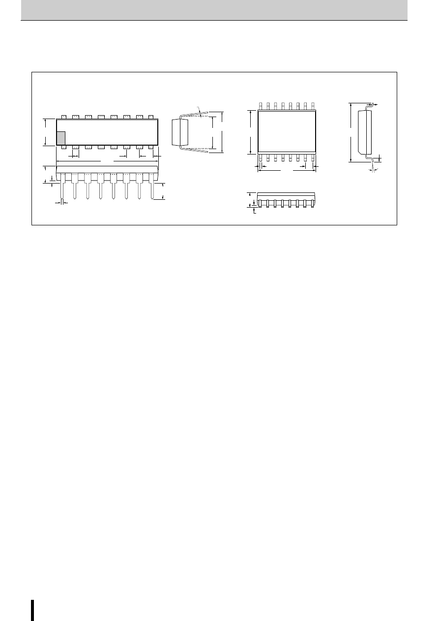
92
A3955SB/SLB
2-Phase Stepper Motor Bipolar Driver ICs (2W1-2 Phase Excitation/Micro-step Support)
A3955SB/SLB
■
External Dimensions
(Unit: mm)
7.11
6.10
5.33
MAX
3.81
2.93
1.77
1.15
0.13
MIN
0.508
0.204
0.39
MIN
0.558
0.356
16
1
8
2.54
BSC
9
19.68
18.67
7.62
BSC
10.92
MAX
0.32
0.23
1.27
0.40
1.27
BSC
0
°
to 8
°
10.65
10.00
7.60
7.40
2.65
2.35
0.51
0.33
1
16
9
2
3
0.10 MIN.
10.50
10.10
A3955SB
A3955SLB
ac/Allegro/Allegro_Motor_Drive_ICs-html.html

93
A3955SB/SLB
ac/Allegro/Allegro_Motor_Drive_ICs-html.html
94
A3957SLB
2-Phase Stepper Motor Bipolar Driver IC
A3957SLB
■
Features
●
Maximum output ratings: 50V,
±
1.5A
●
Internal 4-bit non-linear DAC for 16-division
microstepping enables 4W1-2, 2W1-2, W1-
2, 2-phase excitation drive without exter-
nal sine wave generator
●
Internal PWM current control in Mixed De-
cay mode (can also be used in Fast Decay
and Slow Decay mode), which improves
motor current response and stability with-
out deterioration of motor iron loss
●
External RC filter for sense terminal not
required thanks to internal blanking circuitry
●
Internal thermal shutdown, crossover-cur-
rent protection and transient-suppression
diodes
●
Special power-up and power-down se-
quencing for motor supply and logic sup-
ply not required
●
Employs copper batwing lead frame with
low thermal resistance
■
Absolute Maximum Ratings
Parameter
Symbol
Ratings
Units
Load supply voltage
V
BB
50
V
Output current (continuous)
I
O
±
1.5
A
Logic supply voltage
V
CC
7.0
V
Logic/reference input
V
IN
−
0.3 to V
CC
+0.3
V
voltage range
Sense voltage
V
S
1.0
V
Package power dissipation P
D
(Note1)
2.23
W
Operating temperature
T
a
−
20 to +85
°
C
Junction temperature
T
j
(Note2)
+150
°
C
Storage temperature
T
stg
−
55 to +150
°
C
●
Output current rating may be limited by duty cycle, ambient temperature, and heat sinking. Under any
set of conditions, do not exceed the specified current rating or a junction temperature of 150
°
C.
Note 1: When ambient temperature is 25
°
C or over, derate using
−
17.86mW/
°
C.
Note 2: Fault conditions where junction temperature (T
j
) exceeds 150
°
C will activate the device’s thermal
shutdown circuitry. These conditions can be tolerated but should be avoided.
Allegro MicroSystems product
■
Terminal Connection Diagram
■
Derating
1
2
3
4
5
6
7
8
9
10
11
12
24
23
22
21
20
19
18
17
16
15
14
13
N.C.
PFD
REF
N.C.
RC
GROUND
GROUND
D3
V
CC
PHASE
D2
N.C.
N.C.
(TOP VIEW)
V
BB
OUTB
N.C.
D0
GROUND
GROUND
SENSE
N.C.
OUTA
N.C.
D1
3
2.5
2
Allo
w
a
b
le pac
kage po
w
e
r dissipation P
D
[W]
1.5
1
0.5
0
Ambient temperature Ta (
°
C)
−
20
0
20
40
60
80
100
A3957S
LB
56
°
C/W
4W1-2 Phase Excitation/Micro-step Support
ac/Allegro/Allegro_Motor_Drive_ICs-html.html
95
A3957SLB
2-Phase Stepper Motor Bipolar Driver IC (4W1-2 Phase Excitation/Micro-step Support)
A3957SLB
■
Electrical Characteristics
(Unless specified otherwise, T
a
=25
°
C, V
BB
=5V to 50V, V
CC
=4.5V to 5.5V)
Parameter
Symbol
Conditions
Limits
Units
min
typ
max
Power outputs (OUT
A
or OUT
B
)
Load supply voltage range
V
BB
Operating, I
O
=
±
1.5A, L=3mH
Vcc
50
V
Output leakage current
I
CEX
V
O
=V
BB
<1.0
50
µ
A
V
O
=0V
<
−
1.0
−
50
µ
A
V
SENSE
=1.0V : Source Driver, I
O
=
−
0.85A
1.0
1.2
V
Output saturation voltage
V
CE (sat)
V
SENSE
=1.0V : Source Driver, I
O
=
−
1.5A
1.4
1.5
V
V
SENSE
=1.0V : Sink Driver, I
O
=0.85A
0.5
0.7
V
V
SENSE
=1.0V : Sink Driver, I
O
=1.5A
1.2
1.5
V
Sense current offset
I
SO
I
S
−
I
O
, I
O
=0.85A, V
S
=0V, V
CC
=5V
20
30
40
mA
Clamp diode forward voltage
V
F
I
F
=0.85A
1.2
1.4
V
I
F
=1.5A
1.5
1.7
V
Motor supply current (No load)
I
BB (ON)
2.0
4.0
mA
I
BB (OFF)
D
0
=D
1
=D
2
=D
3
=0.8V
1.0
50
µ
A
Control logic
Logic supply voltage range
V
CC
Operating
4.5
5.0
5.5
V
Reference voltage range
V
REF
Operating
0.5
2.5
V
UVLO enable threshold
V
UVLOen
V
CC
=0
→
5V
3.35
3.70
4.05
V
UVLO hysteresis
V
UVLOhys
0.25
0.40
0.55
V
Logic supply current
I
CC (ON)
42
50
mA
I
CC (OFF)
D
0
=D
1
=D
2
=D
3
=0.8V
14
17
mA
Logic input voltage
V
IH
2.0
V
V
IL
0.8
V
Logic input current
I
IH
V
IN
=2.0V
<1.0
20
µ
A
I
IL
V
IN
=0.8V
<
−
2.0
−
200
µ
A
Slow Decay Mode
3.5
V
Mixed Decay comparator trip point
V
PFD
Mixed Decay Mode
1.2
2.9
V
Fast Decay Mode
0.8
V
Mixed Decay comparator input offset voltage
V
IO (PFD)
0
±
20
mV
Mixed Decay compartor hysteresis
∆
V
IO (PFD)
5
25
55
mV
Reference input current
I
REF
V
REF
=0V to 2.5V
±
5.0
µ
A
Reference divider ratio
V
REF
/V
S
at trip, D
0
=D
1
=D
2
=D
3
=2V
3.0
DAC accuracy *1
DAC
ERR
V
REF
=1.0V to 2.5V
±
3.0
%
V
REF
=0.5V to 1.0V
±
4.0
%
Current-sense comparator input offset voltage *1
V
IO (S)
V
REF
=0V
−
16
mV
D
1
=D
2
=D
3
=0.8V
0
%
D
0
=0.8V, D
1
=2.0V, D
2
=D
3
=0.8V
17.4
%
D
0
=D
1
=2.0V, D
2
=D
3
=0.8V
26.1
%
D
0
=D
1
=0.8V, D
2
=2V, D
3
=0.8V
34.8
%
D
0
=2.0V, D
1
=0.8V, D
2
=2.0V, D
3
=0.8V
43.5
%
D
0
=0.8V, D
1
=D
2
=2.0V, D
3
=0.8V
52.2
%
D
0
=D
1
=D
2
=2.0V, D
3
=0.8V
60.9
%
Step reference current ratio
SRCR
D
0
=D
1
=D
2
=0.8V, D
3
=2.0V
69.6
%
D
0
=2.0V, D
1
=D
2
=0.8V, D
3
=2.0V
73.9
%
D
0
=0.8V ,D
1
=2.0V, D
2
=0.8V, D
3
=2.0V
78.3
%
D
0
=D
1
=2.0V, D
2
=0.8V, D
3
=2.0V
82.6
%
D
0
=D
1
=0.8V, D
2
=D
3
=2.0V
87.0
%
D
0
=2.0V, D
1
=0.8V, D
2
=D
3
=2.0V
91.3
%
D
0
=0.8V, D
1
=D
2
=D
3
=2.0V
95.7
%
D
0
=D
1
=D
2
=D
3
=2.0V
100
%
Thermal shutdown temperature
T
j
165
°
C
Thermal shutdown hysteresis
∆
T
j
15
°
C
AC timing
PWM RC fixed off-time
t
OFFRC
C
T
=470pF, R
T
=43k
Ω
18.2
20.2
22.3
µ
S
Current-Sense Comparator Trip to Source OFF,
PWM turn-off time
t
PWM (OFF)
I
O
=0.1A
1.0
1.5
µ
S
Current-Sense Comparator Trip to Source OFF,
I
O
=1.5A
1.4
2.5
µ
S
PWM turn-on time
t
PWM (ON)
I
RC
Charge ON to Source ON, I
O
=0.1A
0.4
0.7
µ
S
I
RC
Charge ON to Source ON, I
O
=1.5A
0.55
0.85
µ
S
PWM minimum on-time
t
ON (min)
V
CC
=5.0V, R
T
≥
43k
Ω
, C
T
=470pF,
1.0
1.6
2.2
µ
S
I
O
=0.1A
Crossover dead time
t
CODT
1k
Ω
Load to 25V
0.3
1.5
3.0
µ
S
*1: The total error for the V
REF
/V
SENSE
function is the sum of the D/A error and the current-sense comparator input offset voltage.
●
“typ” values are for reference.
ac/Allegro/Allegro_Motor_Drive_ICs-html.html
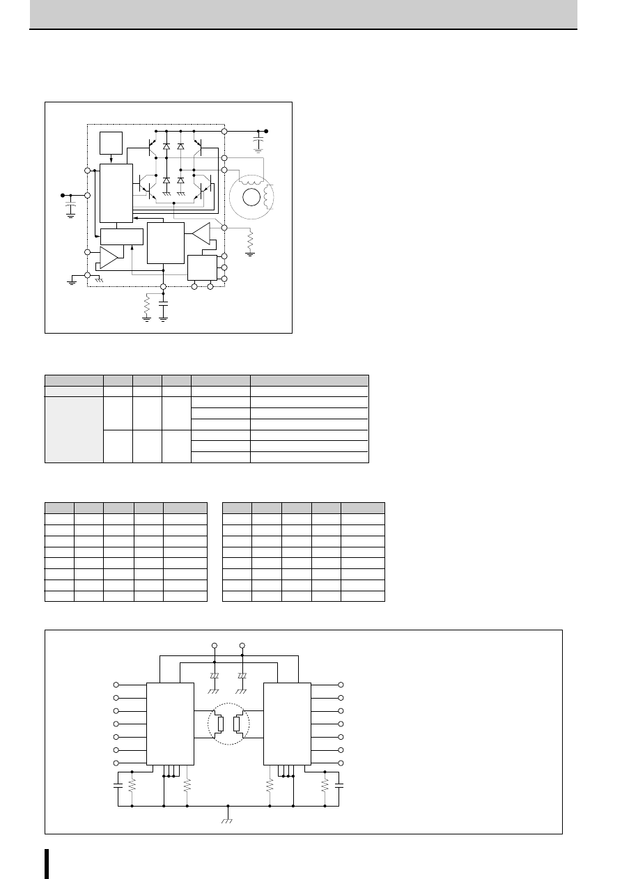
96
A3957SLB
2-Phase Stepper Motor Bipolar Driver IC (4W1-2 Phase Excitation/Micro-step Support)
A3957SLB
■
Application Circuit
●
Off-time setting : t
OFF
≅
R
T
•
C
T
R
T
=36
Ω
(12k
Ω
to 100k
Ω
)
C
T
=560pF (470pF to 1500pF)
R
S
=0.51
Ω
(0.39
Ω
to 0.62
Ω
)
C
BB
=100
µ
F+0.1
µ
F
C
CC
=0.1
µ
F
V
REF
=0.5V to 2.5V
V
PFD
=1.2V to 2.9V (Mixed current-decay mode)
≥
3.5V (Slow current-decay mode)
≤
0.8V (Fast current-decay mode)
+
+
Phase1
10
9
9
23
23
20
13
11
A3957SLB
6,7,
18,19
A3957SLB
6,7,
18,19
8
3
2
10
20
13
11
8
3
2
5
5
17
17
15
C
BB
VBB
Vcc
C
CC
22
15
22
D10
D11
D12
D13
REF1
PFD1
Phase2
D20
D21
D22
D23
REF2
PFD2
CT1
CT2
RT1
RT2
Rs
Rs
■
Internal Block Diagram
+
−
+
−
PFD
PHASE
V
CC
OUT
B
V
BB
MOTOR
SUPPLY
OUT
A
GND
RC
(000X)
D0
16
LEVEL
DAC
BLANKING
TIME AND
DRIVER
T
OFF
CONTROL
DECAY MODE
CONTROL
CONTROL
LOGIC
AND
LEVEL
SHIFT
UVLO
AND
TSD
D2
D3
REF
SENSE
D1
R
T
R
S
C
BB
C
T
Power Outputs
D3, D2, D1, D0
PHASE OUTA
OUTB
PFD
Power Output Operating Mode
0000 or 0001
X
Z
Z
X
Disable
≥
3.5V
Forward, slow current-decay mode
H
H
L
1.2V to 2.9V
Forward, mixed current-decay mode
≤
0.8V
Forward, fast current-decay mode
≥
3.5V
Reverse, slow current-decay mode
L
L
H
1.2V to 2.9V
Reverse, mixed current-decay mode
≤
0.8V
Reverse, fast current-decay mode
X: Don’t care
High impedance (source and sink both OFF)
■
Truth Table
DAC
D3
D2
D1
D0
DAC [%]
1
1
1
1
100
1
1
1
0
95.7
1
1
0
1
91.3
1
1
0
0
87.0
1
0
1
1
82.6
1
0
1
0
78.3
1
0
0
1
73.9
1
0
0
0
69.6
1XXX
or
X1XX
or
XX1X
D3
D2
D1
D0
DAC [%]
0
1
1
1
60.9
0
1
1
0
52.2
0
1
0
1
43.5
0
1
0
0
34.8
0
0
1
1
26.1
0
0
1
0
17.4
0
0
0
1
0
0
0
0
0
0
ac/Allegro/Allegro_Motor_Drive_ICs-html.html
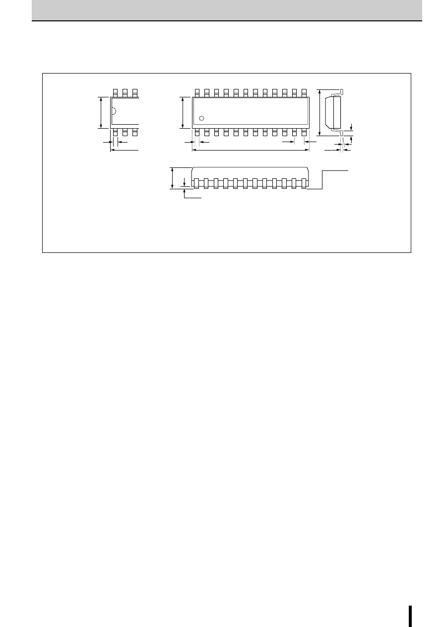
97
A3957SLB
2-Phase Stepper Motor Bipolar Driver IC (4W1-2 Phase Excitation/Micro-step Support)
A3957SLB
■
External Dimensions
(Unit: mm)
15.2/15.6
0.23/0.32
24
19
1
24
*1
1
0.33/0.51
0.33/0.51
0.10MIN
1.27
BSC
2.35/2.65
7.40/7.60
10.0/10.65
7.40/7.60
SEATING
PLANE
0
°
/ 8
°
0.40/1.27
●
●
●
●
Pin material: copper, pin surface treatment: solder plating
Package index may be *1.
Allowable variation in distance between
leads is not cumulative.
Web (batwing) type lead frames are used for pin
6, 7, 18, 19. The pins are connected to GND.
ac/Allegro/Allegro_Motor_Drive_ICs-html.html
98
SI-7600/SI-7600D
3-Phase Stepper Motor Driver ICs
SI-7600/SI-7600D
■
Electrical Characteristics
■
Recommended Operating Voltage Ranges
■
Absolute Maximum Ratings
Parameter
Symbol
Ratings
Units
Load supply voltage
V
BB
50
V
Logic supply voltage
V
CC
7
V
Input voltage
V
IN
−
0.3 to V
CC
V
Reference input voltage
V
REF
−
0.3 to V
CC
V
Sense voltage
V
sense
1.5
V
Package power dissipation
P
D
1
W
Junction temperature
T
j
−
20 to +85
°
C
Operating temperature
T
op
+125
°
C
Storage temperature
T
stg
−
55 to +125
°
C
Parameter
Symbol
Ratings
Units
Conditions
min
typ
max
Load supply voltage
V
BB
15
45
V
Logic supply voltage
V
CC
3.0
5.5
V
V
OL1
8
15
V
V
OL2
0
1
V
Output voltage
V
OH1
V
BB
−
15
V
BB
−
8
V
V
OH2
V
BB
−
1
V
BB
V
Load supply current
I
BB
25
mA
V
CC
=5.5V
Logic supply current
I
CC
10
mA
V
CC
=5.5V
Logic input voltage
V
IH
3.75
V
V
IL
1.25
V
Logic input current
I
IH
20
µ
A
V
IN
=V
CC
×
0.75
I
IL
−
20
µ
A
V
IN
=V
CC
×
0.25
Maximum clock frequency
F
200
kHz
Edge=0V
100
Edge=V
CC
V
Slow
1.7
V
CC
V
PFD input voltage
V
Mix
0.7
1.3
V
V
Fast
0.3
V
PFD input current
I
PFD
±
50
µ
A
Reference input voltage
V
REF
0
V
CC
−
2
V
Reference input current
I
REF
±
10
µ
A
V
REF
=0~Vcc
−
2V
Sense voltage
V
S1
V
REF
×
0.2
V
Mode=V
CC
, V
REF
=0~V
CC
−
2V
V
S2
V
REF
×
0.17
V
Mode=0V, AV
REF
=0~V
CC
−
2V
RC source current
I
RC
220
µ
A
Off time
T
off
1.1
×
R
t
×
C
t
Sec.
Parameter
Symbol
Ratings
Units
Load supply voltage
V
BB
15 to 45
V
Logic supply voltage
V
CC
3 to 5.5
V
Reference input voltage
V
REF
0.2 to Vcc
−
2
V
(Ta=25
°
C)
Star Connection/Delta Connection
ac/Allegro/Allegro_Motor_Drive_ICs-html.html
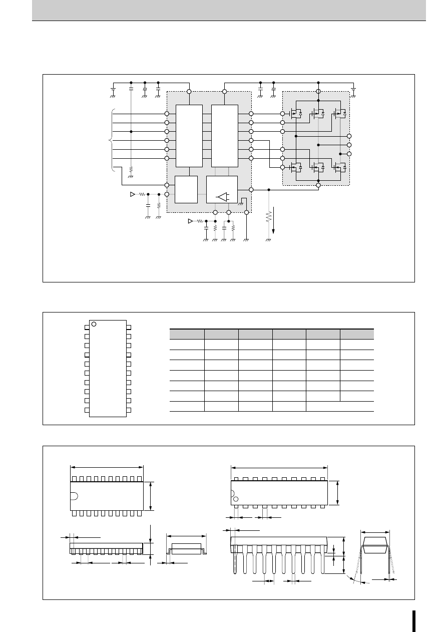
99
SI-7600/SI-7600D
3-Phase Stepper Motor Driver ICs (Star Connection/Delta Connection)
SI-7600/SI-7600D
■
Internal Block Diagram/Diagram of Standard External Circuit
■
Terminal Connection
The package shapes of SI-7600 and SI-7600D are different, however the terminal connection is the same.
■
External Dimensions
(Unless specified otherwise, all values are typical)
(Units: mm)
Pin No.
Name
Pin No.
Name
Pin No.
Name
Pin1
PFD
Pin8
Full/Half
Pin15
OLA
Pin2
Sense
Pin9
Enable
Pin16
OHC
Pin3
Vcc
Pin10
Mode
Pin17
OHB
Pin4
Reset
Pin11
REF
Pin18
OHA
Pin5
CW/CCW
Pin12
GND
Pin19
V
BB
Pin6
Edge
Pin13
OLC
Pin20
RC
Pin7
Clock
Pin14
OLB
+
+
C7
C1
R5
R1
REF
PFD
RC
GND
R2
Rs
MOS Array
ex. SLA5017 at 4A max
SLA5059 at 4A max
SLA5060 at 6A max
SLA5061 at 10A max
(Sanken)
Rt
R4
R3
Ct
C6
Io
C5
C3
C4
OHA
OHB
OHC
OLA
U
V
W
OLB
OLC
Sense
Clock
CW/CCW
Reset
F/H
Ena
Edge
Mode
C2
Vcc
Vcc
Vcc
Reference constants
Rs:0.1 to 1
Ω
(1 to 5W)
Rt:15k to 75k
Ω
Ct:420p to 1100pF
C1:10 F/10V
C2:100 F/63V
C3 to C6:0.01 to 1 F
C7:1000pF
R1+R2
≤
10k
Ω
(V
REF
:0.2 to V
CC
2-2V)
R3+R4
≤
10k
Ω
(V
PFD
:0 to V
CC
2)
R5:10k
Ω
V
BB
Current
Control
Control signal
Pri-
Buffer
Control
Logic
1/5
Buffer
µ
µ
µ
PFD
RC
S
VBB
Vcc
OHA
Reset
OHB
CW/CCW
OHA
EDGE
OLA
CK
OLB
F/H
OLC
Ena
GND
Mode
REF
12.6
7.8
11
20
10
1
0
°
to 15
°
0.48
2.54
1.27 max
0.8 max
0.7
0.4
1.27
0.25
7.62
20
1
11
10
24.50
0.51 min
2.54 min
5
.08 max
6.30
5.5
2.2
max
0.89
SI-7600D
SI-7600
1.30
ac/Allegro/Allegro_Motor_Drive_ICs-html.html
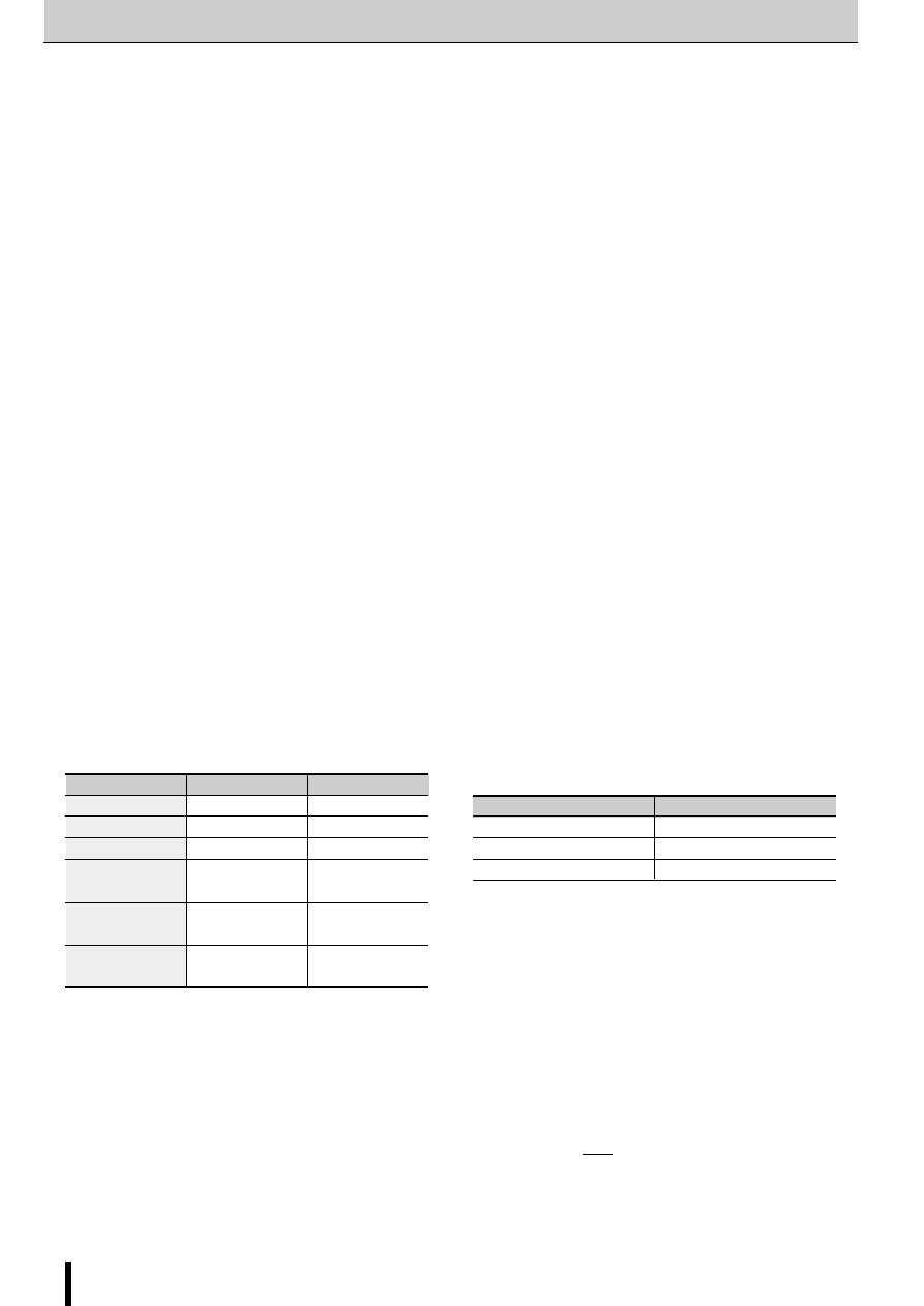
100
SI-7600/SI-7600D
3-Phase Stepper Motor Driver ICs (Star Connection/Delta Connection)
SI-7600/SI-7600D
1. Outline
The SI-7600/SI-7600D is a control IC used with a power MOS
FET array to drive a 3-phase stepper motor. Select the output-
stage MOS FET according to the rated current of the motor.
The full step is 2-phase excitation when this IC is in a star con-
nection but 3-phase excitation when it is in a delta connection.
2. Features
●
Suitable for both star connection drive and delta connection drive
●
Maximum load supply voltage V
BB
=45V
●
Control logic supply voltage Vcc=3 to 5.5V
●
Supports star connection (2/2-3phase excitation) and delta
connection (3/2-3phase excitation)
●
Step switching timing by clock signal input
●
Forward/reverse, hold, and motor-free control
●
Step switching at the positive edge or positive/negative edge
of the clock signal
●
Control current automatic switching function for 2-3phase ex-
citation (effective for star connection)
(Current control: 86% for 2-phase excitation, 100% for 3-phase
excitation)
●
Self-excitation constant-current chopping by external C/R
●
Slow Decay, Mixed Decay, or Fast Decay selectable
●
Two package lineup: SOP (surface mounting) and DIP (lead
insertion)
SOP
…
SI-7600, DIP
…
SI-7600D
●
Maximum output current depends on the ratings of the MOS
FET array used
3. Input Logic Truth Table
Input terminal
Low level
High level
CW/CCW
CW
CCW
Full/Half
2-3phase excitation
2-phase excitation
Enable
Disable
Enable
Mode
Always 100%
2-phase excitation: 85%
(Note 1)
3-phase excitation: 100%
Edge
Positive
Positive/negative
(Note 2)
Reset
Enable
Internal logic reset
(Note 3)
output disable
Select CW/CCW, Full/Half, or Edge when the clock level is low.
Note 1: The control current is always 85% for the full step (2-
phase excitation) when the Mode terminal level is high.
The value of 100% control current is calculated at the
V
REF
/(5
×
Rs) terminal because a 1/5 buffer is built into
the reference section.
Note 2: When the Edge terminal level is set high, the internal
counter increments both at the rising and falling edges.
Therefore, the duty ratio of the input clock should be set
at 50%.
Note 3: When the Reset terminal level is set high, the internal
counter is reset. Output remains disabled as long as the
Reset terminal level is high.
4. Determining the control current
The control current Io can be calculated as follows:
When the Mode terminal level is low
I
O
≅
V
REF
/(5
×
R
S
)
When the Mode terminal level is high
I
O
≅
V
REF
/(5
×
R
S
)
→
3-phase excitation
I
O
≅
V
REF
/(5.88
×
R
S
)
→
2-phase excitation
The reference voltage can be set within the range of 0.2V to Vcc
−
2V.
(When the voltage is less than 0.2V, the accuracy of the refer-
ence voltage divider ratio deteriorates.)
5. About the Current Control System (Setting the
Constant Ct/Rt)
The SI-7600 uses a current control system of the self-excitation
type with a fixed chopping OFF time.
The chopping OFF time is determined by the constant Ct/Rt.
The constant Ct/Rt is calculated by the formula
T
OFF
≅
1.1
×
Ct
×
Rt
……
(1)
The recommended range of constant Ct/Rt is as follows:
Ct: 420 to 1100pF
Rt: 15 to 75k
Ω
(Slow Decay or Mixed Decay
→
560pF/47k
Ω
, Fast Decay
→
470pF/20k
Ω
)
Usually, set T
OFF
to a value where the chopping frequency be-
comes about 30 to 40kHz.
The mode can be set to Slow Decay, Fast Decay, or Mixed De-
cay depending on the PFD terminal input potential.
PFD applied voltage and decay mode
PFD applied voltage
Decay mode
0 to 0.3V
Fast Decay
0.7V to 1.3V
Mixed Decay
1.7V to Vcc
Slow Decay
In Mixed Decay mode, the Fast/Slow time ratio can be set using
the voltage applied to the PFD terminal. The calculated values
are summarized below.
In this mode, the point of switching from Fast Decay to Slow
Decay is determined by the RC terminal voltage that determines
the chopping OFF time and by the PFD input voltage V
PFD
.
Formula (1) is used to determine the chopping OFF time.
The Fast Decay time is then determined by the RC discharge
time from the RC voltage (about 1.5V) to the PFD input voltage
(V
PFD
) when chopping is turned from ON to OFF.
The Fast Decay time is
……
(2)
The Slow Decay time (t
OFFs
) is calculated by subtracting the value
of (2) from that of (1).
t
OFFS
≅
T
OFF
−
t
OFFf
……
(3)
Application Notes
t
OFFf
≅−
R
T
×
C
T
×
l
n
( )
V
PFD
1.5
ac/Allegro/Allegro_Motor_Drive_ICs-html.html
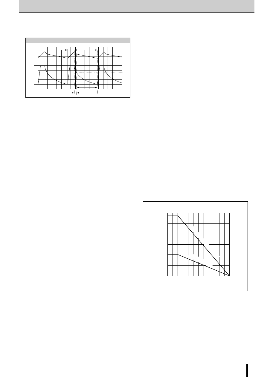
101
SI-7600/SI-7600D
3-Phase Stepper Motor Driver ICs (Star Connection/Delta Connection)
SI-7600/SI-7600D
Ton
Toff
ITrip
I
OUT
1.5V
V
RC
0.5V
Fast
Decay
V
PFD
Slow Decay
15
5
10
0
25
0
50
75
Ambient temperature Ta (
°
C)
(W)
100
125
150
P
o
w
e
r dissipation P
Without heatsink
100
×
100
×
2mm Al heatsink
6. Method of Calculating Power Loss of Output
MOS FET
The SI-7600 uses a MOS-FET array for output. The power loss
of this MOS FET array can be calculated as summarized below.
This is an approximate value that does not reflect parameter
variations or other factors during use in the actual application.
Therefore, heat from the MOS FET array should actually be
measured.
●
Parameters for calculating power loss
To calculate the power loss of the MOS FET array, the following
parameters are needed:
(1) Control current Io (max)
(2) Excitation method
(3) Chopping ON-OFF time at current control: T
ON
, T
OFF
, t
OFFf
(T
ON
: ON time, T
OFF
: OFF time, t
OFFf
: Fast Decay time at OFF)
(4) ON resistance of MOS FET: R
DS (ON)
(5) Forward voltage of MOS FET body diode: V
SD
For (4) and (5), use the maximum values of the MOS FET speci-
fications.
(3) should be confirmed on the actual application.
●
Power loss of Pch MOS FETs
The power loss of Pch MOS FETs is caused by the ON resis-
tance and by the chopping-OFF regenerative current flowing
through the body diodes in Fast Decay mode.
(In Slow Decay mode, the chopping-OFF regenerative current
does not flow the body diodes.)
The losses are
ON resistance loss P1: P1=I
M
2
×
R
DS (ON)
Body diode loss P2: P2=I
M
×
V
SD
With these parameters, the loss Pp per MOS FET is calculated
depending on the actual excitation method as follows:
a) 2-phase excitation (T=T
ON
+T
OFF
)
P
P
= (P1
×
T
ON
/T+P2
×
t
OFFf
/T)
×
(1/3)
b) 2-3 phase excitation (T=T
ON
+T
OFF
)
P
P
= (P1
×
T
ON
/T+P2
×
t
OFFf
/T)
×
(1/4)+(0.5
×
P1
×
T
ON
/T+P2
×
t
OFFf
/
T)
×
(1/12)
●
Power loss of Nch MOS FETs
The power loss of Nch MOS FETs is caused by the ON resis-
tance or by the chopping-OFF regenerative current flowing
through the body diodes.
(This loss is not related to the current control method, Slow,
Mixed, or Fast Decay.)
The losses are
ON resistance loss N1: N1=I
M
2
×
R
DS(ON)
Body diode loss N2: N2=I
M
×
V
SD
With these parameters, the loss P
N
per MOS FET is calculated
depending on the actual excitation method as follows:
a) 2-phase excitation (T=T
ON
+T
OFF
)
P
N
=(N1+N2
×
T
OFF
/T)
×
(1/3)
b) 2-3 phase excitation (T=T
ON
+T
OFF
)
P
N
=(N1+N2
×
T
OFF
/T)
×
(1/4)+(0.5N1+N2
×
T
OFF
/T)
×
(1/12)
●
Determining power loss and heatsink when SLA5017 is
used
If the SLA5017 is used in an output section, the power losses of
a Pch MOS FET and an Nch MOS FET should be multiplied by
three and added to determine the total loss P of SLA5017.
In other words, P=3
×
P
P
+3
×
P
N
The allowable losses of SLA5017 are
Without heatsink: 5W
θ
j-a=25
°
C/W
Infinite heatsink: 35W
θ
j-c=3.57
°
C/W
Select a heatsink by considering the calculated losses, allow-
able losses, and following ratings:
When selecting a heatsink for SLA5017, be sure to check the
product temperature when in use in an actual applicaiton.
The calculated loss is an approximate value and therefore con-
tains a degree of error.
Select a heatsink so that the surface Al fin temperature of
SLA5017 will not exceed 100
°
C under the worst conditions.
Relationship between RC terminal voltage and output current
ac/Allegro/Allegro_Motor_Drive_ICs-html.html
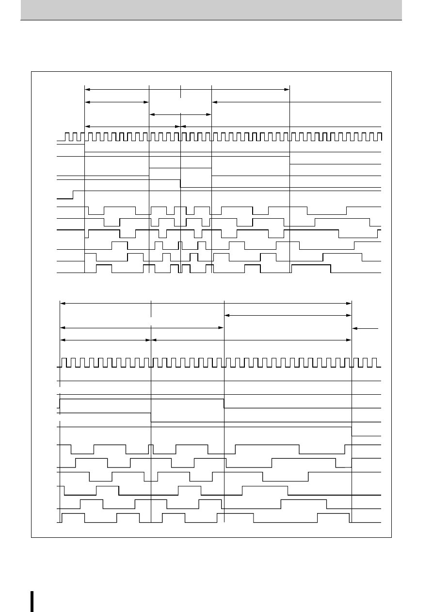
102
SI-7600/SI-7600D
3-Phase Stepper Motor Driver ICs (Star Connection/Delta Connection)
SI-7600/SI-7600D
2-phase excitation
2-3 phase excitation
Positive edge
2-3 phase excitation
Positive edge
Positive edge
Positive/negative edge
Disable
CCW
CK
Reset
Full/Half
EDGE
CW/CCW
Ena
OHA
OHB
OHC
OLA
OLB
OLC
CK
Reset
ED
Ena
OHA
OHB
OHC
OLA
OLB
OLC
CW
CW
CCW
CW/CCW
Full/Half
Positive/negative edge
7. I/O Timing Chart
ac/Allegro/Allegro_Motor_Drive_ICs-html.html

103
SI-7600/SI-7600D
ac/Allegro/Allegro_Motor_Drive_ICs-html.html
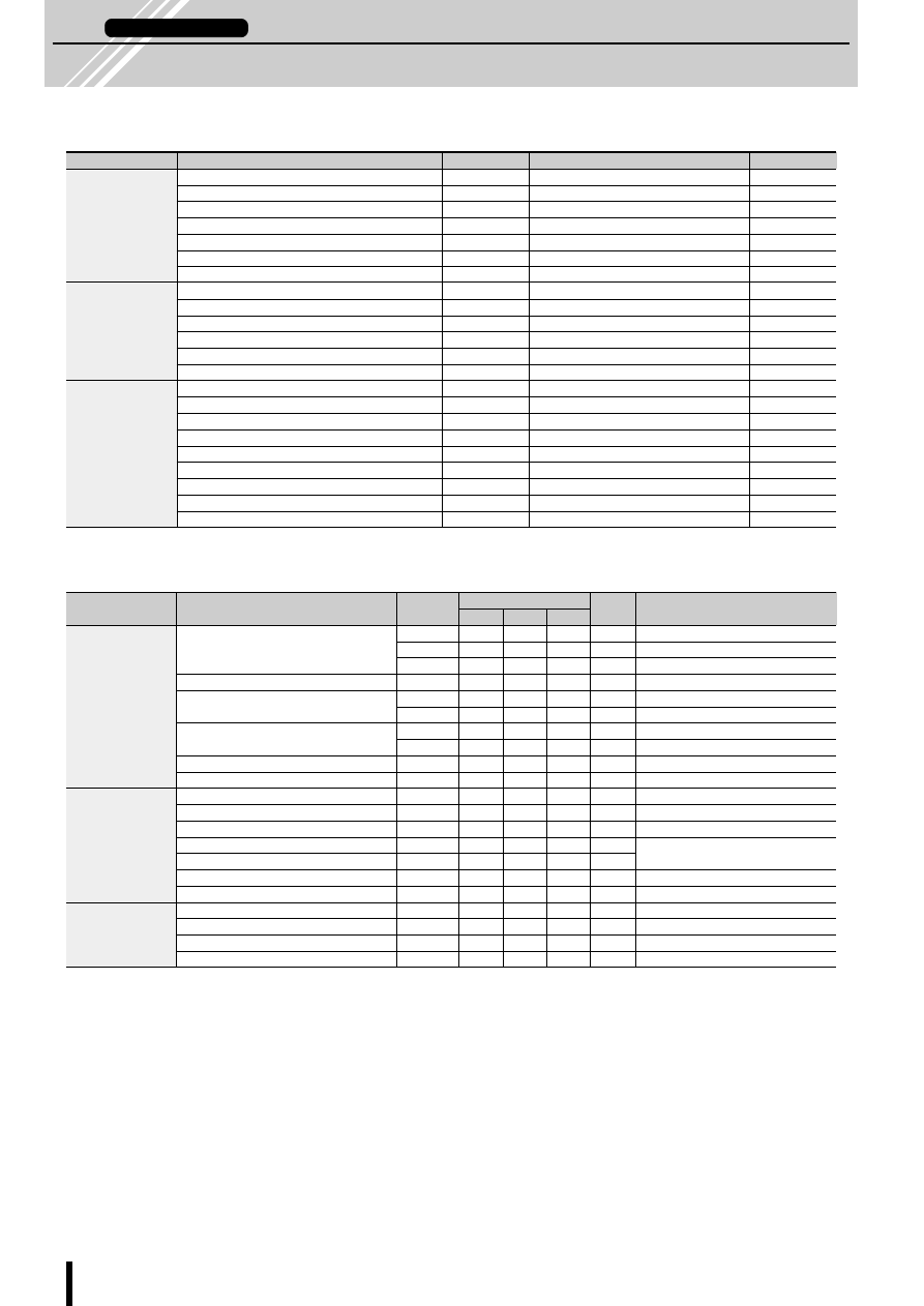
104
SI-7502
(SLA5011/SLA6503)
Part No.
Parameter
Symbol
Ratings
Units
Motor supply voltage
V
CC
44
V
Auxiliary supply voltage
V
S
15
V
Control voltage
V
b
7
V
SI-7502
Reference voltage
V
ref
1.5
V
Detection voltage
V
RS
5
V
Power dissipation
P
D
1
W
Ambient operating temperature
T
OP
0 to +65
°
C
Drain -Source voltage
V
DSS
60
V
Drain current
I
D
±
5
A
SLA5011
Avalanche energy capability (Single pulse)
E
AS
2
mJ
Power dissipation
P
T
35
W
Channel temperature
T
ch
150
°
C
Storage temperature
T
stg
−
40 to +150
°
C
Collector-Base voltage
V
CBO
−
60
V
Collector-Emitter voltage
V
CEO
−
60
V
Emitter-Base voltage
V
EBO
−
6
V
Collector current
I
C
−
3
A
SLA6503
Collector current (Pulse)
I
C (pulse)
−
6
A
Base current
I
B
−
1
A
Power dissipation
P
T
35
W
Junction temperature
T
j
150
°
C
Storage temperature
T
stg
−
40 to +150
°
C
■
Electrical Characteristics
■
Absolute Maximum Ratings
5-Phase Stepper Motor Driver ICs
SI-7502
(SLA5011/SLA6503)
Pentagon Connection
(T
a
=25
°
C)
(T
a
=25
°
C)
Part No.
Parameter
Symbol
Limits
Units
Conditions
min
typ
max
I
CC
40
mA
V
CC
=42V, V
b
=5.5V
Supply current
I
S
12.5
mA
V
S
=12.5V
I
b
50
mA
V
b
=5.5V
Input current
I
IU-L
, I
IL-L
1.6
mA
V
IU
=V
IL
=0.4V
SI-7502
Upper drive circuit drive current
I
OU
-on
8
11
mA
V
b
=5V, AIU to EIU pin open
I
OU
-off
10
µ
A
V
b
=5V
Lower drive circuit voltage
V
OL
-on
V
S
−
1.5
V
V
b
=5V, AIL to EIL pin open
V
OL
-off
1.5
V
V
b
=5V
Oscillation frequency
F
20
30
kHz
V
b
=5V
Detection voltage
V
RS
0.8
1.05
V
V
b
=5V, V
REF
pin open
Gate threshold voltage
V
TH
2.0
4.0
V
V
DS
=10V, I
D
=250
µ
A
Forward Transconductance
R
e (yts)
2.2
3.3
S
V
DS
=10V, I
D
=5A
DC ON-resistance
R
DS (ON)
0.17
0.22
Ω
V
GS
=10V, I
D
=5A
SLA5011
Input capacitance
C
ISS
300
pF
V
DS
=25V, f=1.0MHz,V
GS
=0V
Output capacitance
C
OSS
160
pF
Di forward voltage between source and drain
V
SD
1.1
1.5
V
I
SD
=5A
Di reverse recovery time between source and drain
t
rr
150
ns
I
SD
=
±
100mA
Collector cut-off current
I
CBO
−
10
µ
A
V
CB
=
−
60V
SLA6503
Collector-emitter voltage
V
CEO
−
60
V
I
C
=
−
10mA
DC current gain
h
FE
2000
V
CE
=
−
4V, I
C
=
−
3A
Collector emitter saturation voltage
V
CE (sat)
1.5
V
I
C
=
−
3A, I
B
=
−
6mA
ac/Allegro/Allegro_Motor_Drive_ICs-html.html
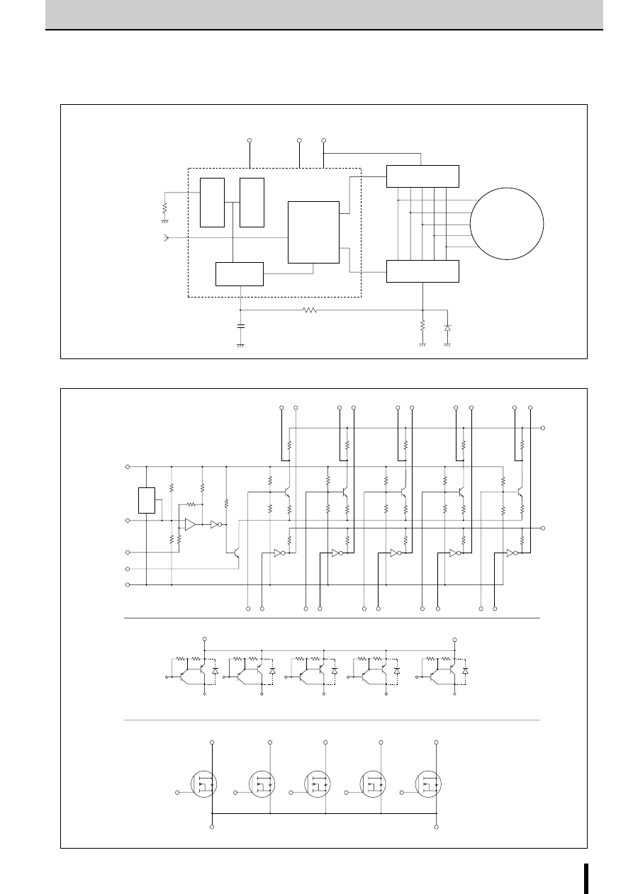
105
SI-7502
(SLA5011/SLA6503)
SI-7502
(SLA5011/SLA6503)
5-Phase Stepper Motor Driver ICs (Pentagon Connection)
■
Internal Block Diagram (Dotted Line)
Control power supply
V
b
V
S
V
CC
Main power supply
SLA6503
SLA5011
Motor
Comparator
amplifier
Excitation signal
Variable current
resistor R
X
Current sense
resistor Rs
SI-7502
Level shift
current control
unit
Auxiliary power
supply
Ref
erence
v
oltage
Tr
igger pulse
gener
ator circuit
■
Equivalent Circuit Diagram
SI-7502
24
20
23
19
16
12
15
11
7
8
27
R21
R20
R19
R18
R17
R1
R3
R4
R6
R5
R2
Tr1
25
21
22
18
17
13
14
10
6
9
R7
Tr2
R12
R22
R27
R13
R23
R8
Tr3
R9
Tr4
R10
Tr5
R11
Tr6
R16
R26
R15
R25
R14
R24
26
R31
R30
R29
R28
SLA6503
R1
R2
2
3
4
1
5
6
7
8
9
10
11
12
R
1
≅
2k
Ω
Typ
R
2
≅
50
Ω
Typ
SLA5011
2
4
5
3
Trigger pulse
generator circuit
−
+
1
12
11
9
7
5
3
10
8
6
4
2
1
ac/Allegro/Allegro_Motor_Drive_ICs-html.html
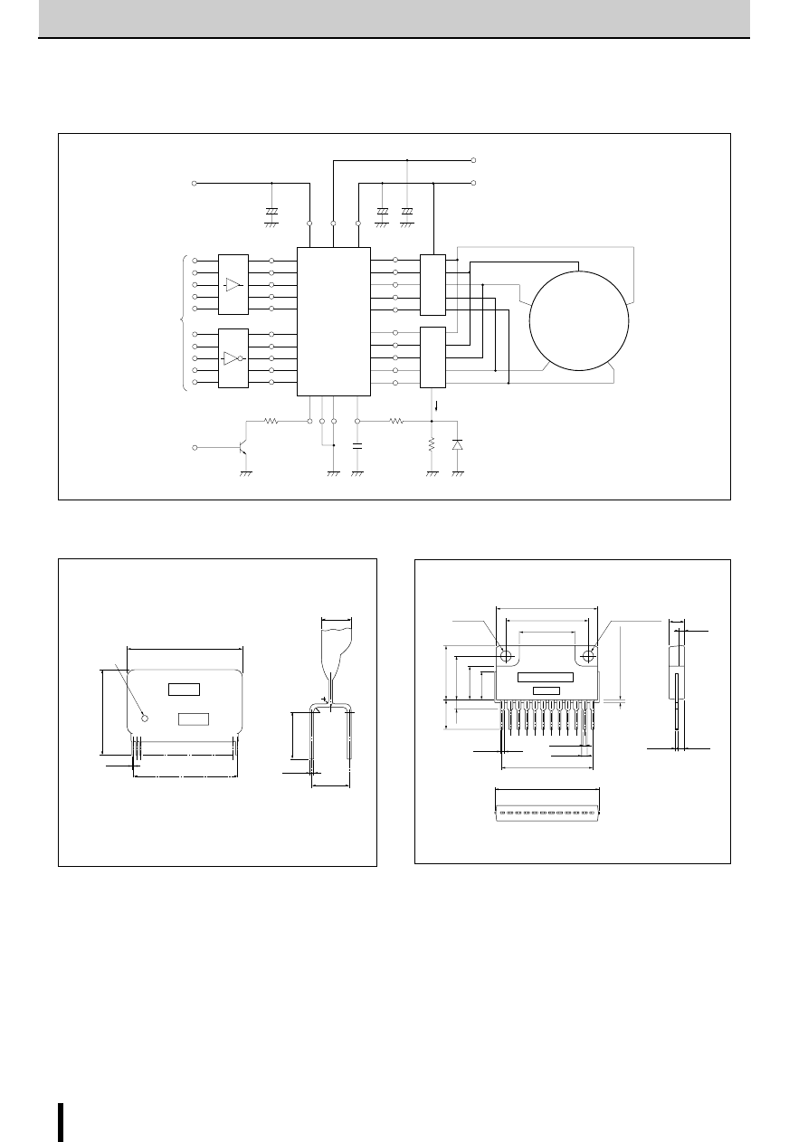
106
SI-7502
(SLA5011/SLA6503)
SI-7502
(SLA5011/SLA6503)
5-Phase Stepper Motor Driver ICs (Pentagon Connection)
41 (max)
#
P1.27
±
0.7
×
26=33.02
0.5
+0.15
−
0.05
1pin
27pin
0.3
+0.15
−
0.05
#
2.54
±
0.6
3.5
+1
−
0.5
27pin
26pin
8(max)
30 (max)
R : 0.3mm
R
R
Pin-1 marking
(White dots)
Lot No.
Part No.
31.0
±
0.2
24.4
±
0.2
16.4
±
0.2
3.2
±
0.15
×
3.8
4.8
±
0.2
1.7
±
0.1
3.2
±
0.15
16.0
±
0.2
13.0
±
0.2
9.9
±
0.2
8.5max.
0.85
+0.2
−
0.1
1.45
±
0.15
11
×
P2.54
±
0.7
=27.94
±
1.0
9.5min (10.4)
1.2
±
0.15
31.5max.
1 2 3 4 5 6 7 8 9 10 11 12
Part No.
Lot No.
0.55
+0.2
−
0.1
2.2
±
0.7
12
Pin 1
2.7
0.8 max
φ
V
B
(5V)
C
3
+
7407
Aiu
Biu
Ciu
Diu
Eiu
Ail
Bil
Cil
Dil
Eil
7406
25
22
17
14
6
21
18
13
10
9
1
26
27
C
1
+ C
2
+
24
23
16
15
7
20
19
12
11
8
2
4
6
8
10
2
4
6
8
10
3
5
7
9
11
3
5
7
9
11
1 12
I
O
V
S
(12V)
V
CC
(15~42V)
A
0
B
0
C
0
D
0
E
0
Stepper Motor
C
1
C
2
C
3
C
4
R
1
D
i
: 100 F/63V
: 50 F/25V
: 10 F/10V
: 470pF
: 1k
Ω
: RK-34 (Sanken)
I
O
(typ)
I
OPD
(typ)
a
R'
= 0.92/R
S
= (1.3
×
a
−
0.01) / Rs
= Vb
×
R' / (30000+R')
= 5100
×
Rx / (5100+Rx)
D
i
R
S
R
1
R
X
P
D
4
5
3
2
C
4
Active High
SI-7502
SLA5011
SLA6503
1
12
Excitation signal input
µ
µ
µ
(Note) Dimensions marked with a # indicate dimensions of
lead tip.
■
Diagram of Standard External Circuit
■
External Dimensions
(Unit: mm)
■
External Dimensions
(Unit: mm)
SI-7502
SLA6503/SLA5011
ac/Allegro/Allegro_Motor_Drive_ICs-html.html
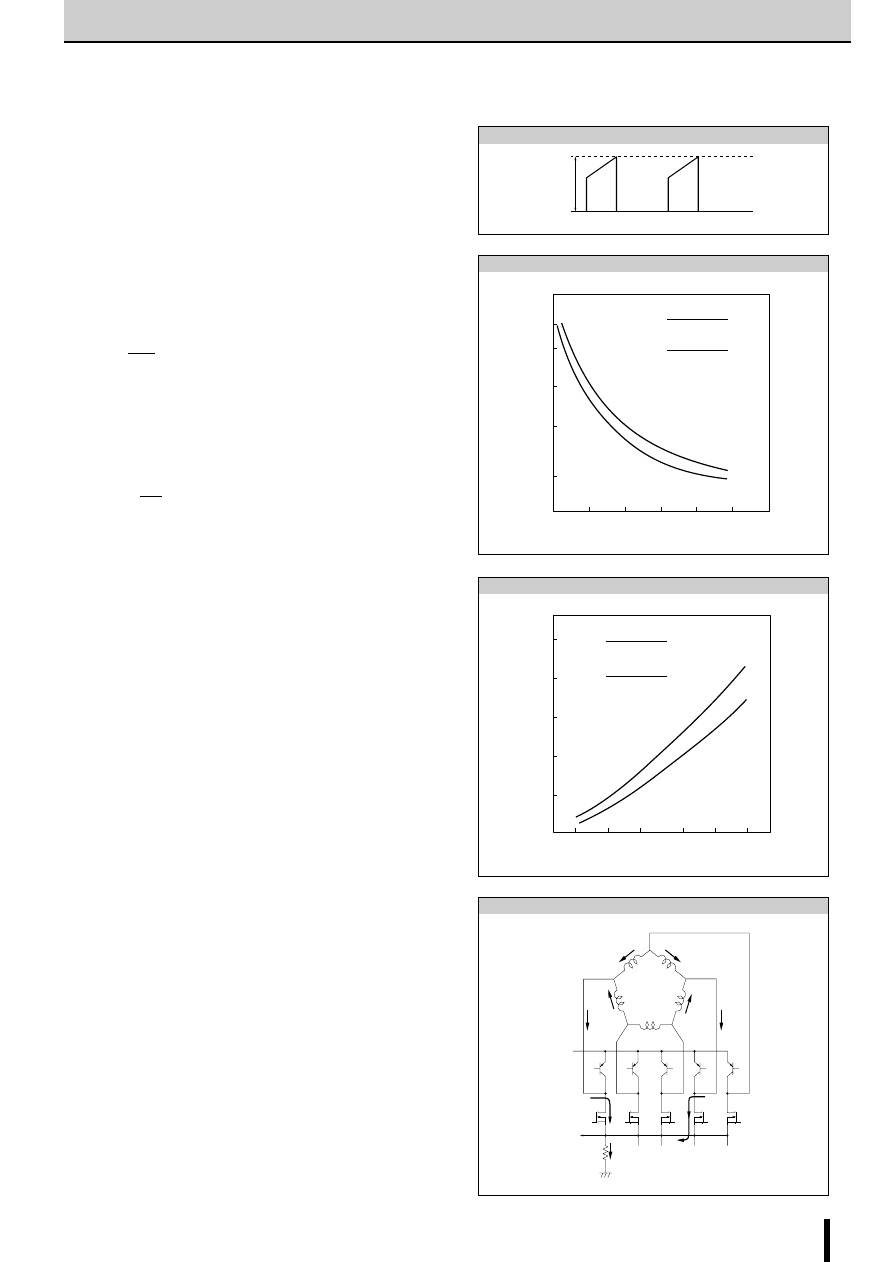
107
SI-7502
(SLA5011/SLA6503)
SI-7502
(SLA5011/SLA6503)
5-Phase Stepper Motor Driver ICs (Pentagon Connection)
Fig. A
Waveform of output current
I
OH
O
I
OH(max)
=
0.212
×
V
b
−
0.01
Rs
I
OH(min)
=
0.169
×
V
b
−
0.03
Rs
I
OH(max)
(V
b
=5V)
I
OH(min)
(V
b
=5V)
1
2
3
4
5
(
Ω
)
(A)
3
2
1
0.5
0.2
Sense resistor Rs
Output current I
OH
V
RSH (max)
=
7.2
×
R
X
152.6+33.8
×
R
X
×
V
b
−
0.01
V
RSH (min)
=
6.1
×
R
X
152.6+33.8
×
R
X
×
V
b
−
0.03
V
RSH (max)
(V
b
=5V)
V
R
SH
(m
in
)
(V
b
=5V)
0.5
1
2
5
10
(K
Ω
)
Variable current resistor Rx
20
0.2
1.0
0.8
0.6
0.4
(V)
Sense voltage V
RSH
I
OM
I
OM
I
OM
I
OM
2
×
I
OM
2
×
I
OM
V
CC
4
×
I
OM
to SI-7502
Sense resistor Rs
Fig. B Output current vs. Current sense resistor
Fig. C Sense voltage vs. Variable current resistor
Fig. D Coil current flow at pentagonal driving
■
Determining the Output Current I
O
(Control Current)
The main factors that determine the output current are current
sense resistor R
S
, supply voltage V
b
, and variable current resis-
tor R
X
.
(1) Normal mode
To operate a motor at the maximum current level, set R
X
to
infinity (open).
From Fig. A, when the maximum current ripple is designated
as I
OH
, its value will be,
V
RSH
can be calculated as follows:
V
RSH
=0.19
×
V
b
−
0.03 (center value)
From equations (1) and (2), the output current I
OH
can be
calculated as follows:
The relationship between I
OH
and R
S
is shown in Fig. B.
(2) Power down mode
When an external resistor R
X
is connected, V
RSH
changes as
shown in Fig. C even when R
S
is retained. Obtain a power
down output current I
OHPD
from Fig. C and equation (1).
■
Relation between Output Current I
O
(Control
Current) and Motor Winding Current I
OM
The SI-7502 uses the total current control system; therefore,
the output current I
O
is different from the motor winding current.
In a general pentagonal driving system, the current flows as
shown in Figure D. The relation between I
O
and I
OM
is as follows:
I
O
=4
×
I
OM
With some driving systems, the relation can also be as follows:
I
O
=2
×
I
OM
V
RSH
R
S
Application Notes
............................... (2)
I
OH
=
...................................................................... (1)
I
OH
= (0.19
×
V
b
×
-0.03)
1
R
S
ac/Allegro/Allegro_Motor_Drive_ICs-html.html
108
SI-7502
(SLA5011/SLA6503)
SI-7502
(SLA5011/SLA6503)
5-Phase Stepper Motor Driver ICs (Pentagon Connection)
−
40
0
50
100
150 (
°
C)
15
10
5
0
Ambient temperature Ta
(W)
50
×
50
×
2 mm
AI FIN
N0 FIN
100
×
100
×
2 mm
AI FIN
Power dissipation P
T
Fig. E SLA5011/SLA6503 Derating curve
■
Motor Connection
The 5-phase stepper motor supports various driving systems
and the motor connection varies depending on the driving sys-
tem used.
Use of the motor with some driving systems may be restricted
by patents. Therefore, be sure to ask the motor manufacturer
about the motor connection and driving system to be used.
■
Thermal design
The driver (SLA5011/SLA6503) dissipation varies depending on
a driving system used even if the output currents (control cur-
rent) are the same. Therefore, measure the temperature rise of
the driver under the actual operating conditions to determine
the size of the heatsink.
Figure E shows an SLA5011/SLA6503 derating curve. This de-
rating curve indicates T
j
=150
°
C; however, when using this de-
vice, allow sufficient margin when selecting a heatsink so that
T
C
≤
100
°
C (AI FIN temperature on the back of the SLA) is ob-
tained.
Substances that can dissolve
the package
Substances that can weaken
the package
SI-7502
■
Handling Precautions
Refer to the product specifications.
Solvents- Do not use the following solvents:
Chlorine-based solvents: Trichloroethylene, Trichloroethane, etc.
Aromatic hydrogen compounds: Benzene, Toluene, Xylene, etc.
Keton and Acetone group solvents
Gasoline, Benzine, Kerosene, etc.
ac/Allegro/Allegro_Motor_Drive_ICs-html.html

109
SI-7502
(SLA5011/SLA6503)
ac/Allegro/Allegro_Motor_Drive_ICs-html.html

110
Part No.
Substitute
SI-7200E
−
SI-7201A
−
SI-7202A
−
SI-7230E
−
SI-7235E
−
SDK01M
SDK03M
SMA7022M
SMA7022MU
SLA7022M
SLA7022MU
SLA7027M
SLA7027MU
■
Discontinued Products
List of Discontinued Products
Part No.
Substitute
SI-7115B
SLA7032M
SI-7300A
SLA7032M
SI-7330A
SLA7033M
SI-7200M
A2918SW
SI-7230M
−
SI-7500A
−
■
Not for new design
List of Discontinued Products
Stepper Motor Driver ICs
ac/Allegro/Allegro_Motor_Drive_ICs-html.html

111
ac/Allegro/Allegro_Motor_Drive_ICs-html.html

112
ac/Allegro/Allegro_Motor_Drive_ICs-html.html
Bulletin No
I02 EB0
(Jul,2000)
K DIC218
SANKEN ELECTRIC COMPANY LTD.
1-11-1 Nishi -Ikebukuro,Toshima-ku, Tokyo
PHONE: 03-3986-6164
FAX: 03-3986-8637
TELEX: 0272-2323(SANKEN J)
Overseas Sales Offices
●
Asia
SANKEN ELECTRIC SINGAPORE PTE LTD.
150 Beach Road #14-03,
The Gateway, West Singapore 0718, Singapore
PHONE: 291-4755
FAX: 297-1744
SANKEN ELECTRIC HONG KONG COMPANY LTD.
1018 Ocean Centre, Canton Road,
Kowloon, Hong Kong
PHONE: 2735-5262
FAX: 2735-5494
TELEX: 45498 (SANKEN HX)
SANKEN ELECTRIC KOREA COMPANY LTD.
SK Life B/D 6F,
168 Kongduk-dong, Mapo-ku, Seoul, 121-705, Korea
PHONE: 82-2-714-3700
FAX: 82-2-3272-2145
●
North America
ALLEGRO MICROSYSTEMS, INC.
115 Northeast Cutoff, Box 15036
Worcester, Massachusetts 01615, U.S.A.
PHONE: (508)853-5000
FAX: (508)853-7861
●
Europe
ALLEGRO MICROSYSTEMS EUROPE LTD.
Balfour House, Churchfield Road,
Walton-on-Thames, Surrey KT12 2TD, U.K.
PHONE: 01932-253355
FAX: 01932-246622
PRINTED in JAPAN H1-I02EB0-0007020ND
Motor Driver ICs