Application
www.diotec.com
1/1
2004-06-22, US
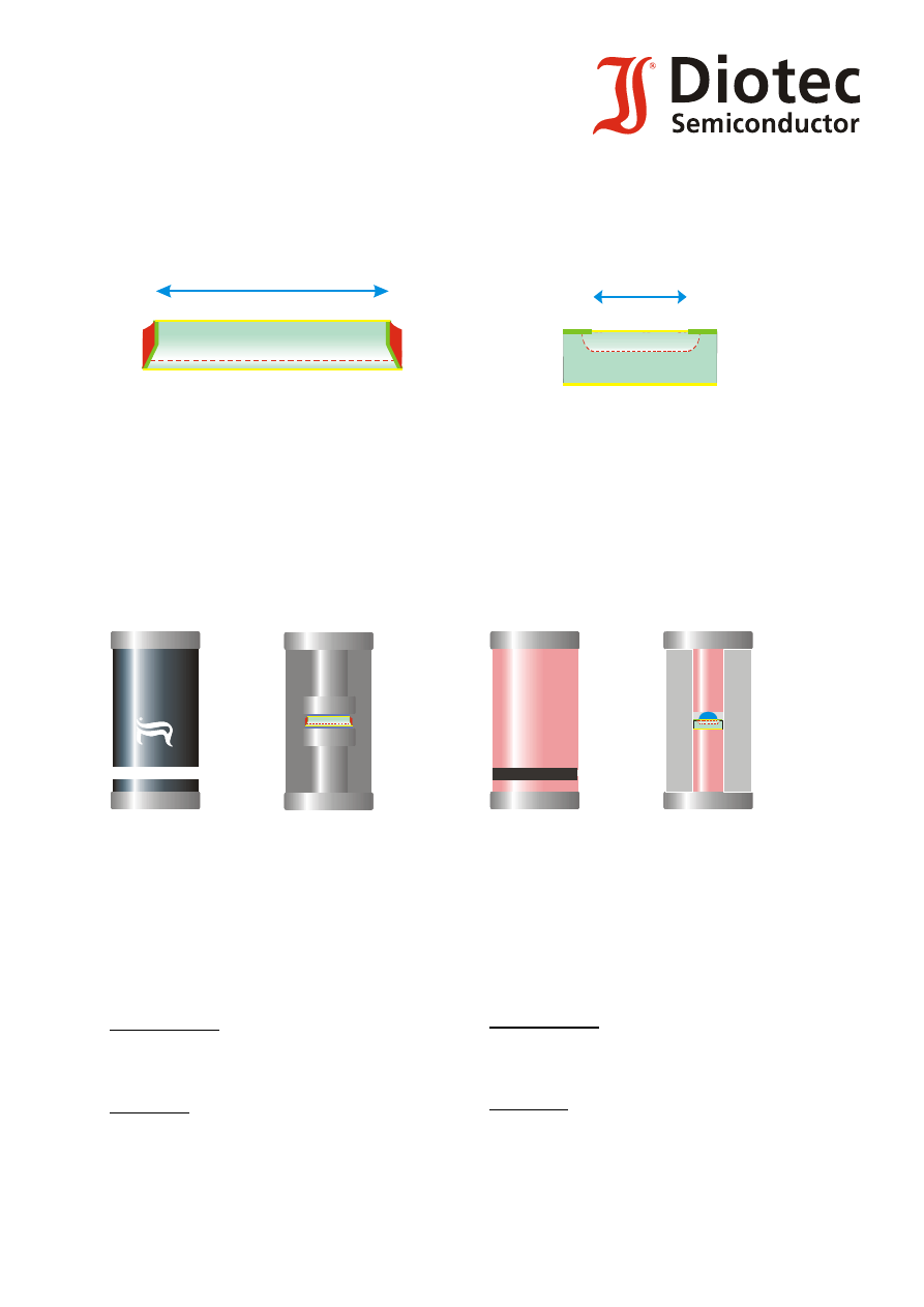
Non-planar
chip technology
n zone top, p zone bottom
large active area (e. g. Melf ~ 1.69 mm
2
)
⇒
Advantages
- High pulse capability
- High power dissipation
- high admissible zener current (Z-diodes)
Assembly: plastic package
Chip soldered to contacts,
molded with duroplast (UL94V-0)
= high reliability and good heat transfer
Application
high currents/power/voltages
e. g.
MiniMELF case
ZMD1…100 (1 W Zener)
GL1A…M (1 A, 50…1000 V)
MELF case
ZMY1…200 (1.3 W Zener)
SMZ1..200 (2 W Zener)
SZ3C1…200 (3 W Zener)
SM513…2000 (1 A, 1.3…2 kV)
Planar
chip technology
p and n zone within one planarity
small active area (e. g. Melf ~ 0.36 mm
2
)
⇒
Advantages
- Low junction capacity
- Low leakage curent I
R
, sharp curve even
for Z-diodes with V
Z
< 6.8 V
Assembly: glass package
Chip pressure contacted,
within glass tube
= simple assembly, but disadvantage
in heat transfer
Application
Small power/small signal diodes
e. g.
MiniMELF case
ZMM1…100 (500 mW Zener)
LL4148 (200 mA, 100 V)
MELF case
ZMY1G…100G (1 W Zener)
Ty
p
e
Ty
p
Ty
p
e
Ty
p
Active area
n
p
Active area
p
n