background image

Datasheet


1/23


TSZ02201-0Q1Q0AJ00150-1-2 

ツゥ 2012 ROHM Co., Ltd. All rights reserved. 

26.Jun.2017 Rev.007 

www.rohm.com 

TSZ22111

繝サ

14

繝サ

001 

Single-chip Type with Built-in FET Switching Regulators


Simple Step-down 
Switching Regulators 
with Built-in Power MOSFET 

BD9G101G 


General Description


The  BD9G101G  is  switching  regulator  with  integrated 
internal high-side 42V Power MOSFET. 
It provides 0.5A DC output with small SSOP6 package. 
Operating  frequency  is  fixed  1.5MHz,  allowing  the  use 
of small inductor and ceramic capacitor. 
The components of phase compensation is built in. 


Features


High and Wide Input Range (VCC=6V~42V) 


45V/800m

ホゥ

  Internal Power MOSFET 


1.5MHz Fixed Operating Frequency 


Feedback Pin Voltage 0.75Vツア1.5% 


Internal compensated 


Internal Over Current protection, Under 
Voltage Locked Out, Thermal shutdown 


0

ホシA Shutdown Supply Current (Ist=0uA) 


Small package SSOP6 


Key Specifications


Input Voltage 


Ref. Precision    (Ta=25

)   

(Ta=-25~105

)


Max Output Current 


Operating Temperature 


Max Junction Temperature 


6

42 [V]   

ツア

1.5[%]   

ツア

2.0[%]   

0.5 [A] (Max.) 

-40

~105


150


Packages


SSOP6 

2.90

緕愿

2.80

緕愿

1.25


Applications


Industrial distributed power applications 


Automotive Applications 


Battery powered equipment 


OA instruments 


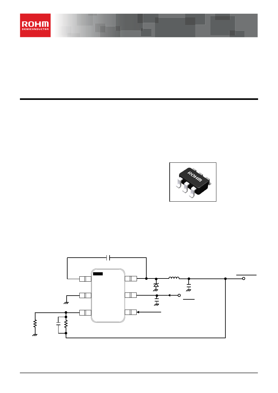
Typical Application Circuits 

VCC

BST

GND

FB

VCC

LX

EN

D1

15000pF

ON/OFF control

C1:4.7ホシF/50V

C2:10ホシF/10V

L1:6.8uH

5V/0.5A

680ホゥ

3.9kホゥ

0.1uF


Structure

Silicon Monolithic Integrated Circuit

  笳

This product is not designed for normal operation with in a radioactive.

Figure 1. Typical Application Circuit 

SSOP6 

bd9g101g-e-html.html
background image


2/23


BD9G101G


TSZ02201-0Q1Q0AJ00140-1-2 

ツゥ 2012 ROHM Co., Ltd. All rights reserved. 

26.Jun.2017 Rev.007 


www.rohm.com 

TSZ22111

繝サ

15

繝サ

001 

Pin Configuration


BST

GND

FB

VCC

LX

EN

1

2

3

4

5

6


Pin Description 


Pin No. 

Pin Name 

Description 

BST 

The pin is power supply for floating Power NMOS driver. Connected a 
bypass capacitor between the pin and Lx pin for bootstrap operation. 

GND 

Ground. It should be connected as possible to the output capacitor ground 
avoiding the high current switch paths. 

FB 

Voltage feedback pin. This pin is error-amp input, the DCDC is set 0.75V at 
this pin with feed-back operation. 

EN 

Enable input pin. The DCDC is start-up to apply over 2.0V.   
This pin is pull-down about 550k

ホゥ, the DCDC is shutdown to open or apply   

under 0.8V. 

VCC 

Input supply. It should be connected as near as possible to the bypass 
capacitor. 

LX 

Power FET switch output. It should be connected as near as possible to the   
schottky barrier diode, and inductor. 


Block Diagram 

EN

0.75V

Error

AMP

VCC

LX

Reference

UVLO

VREF

REG

800mホゥ

Soft

Start

ON/OFF

GND

+

-

+

FB

BST

TSD

shutdown

R縲縲Q
S縲縲縲

Current

Comparator

VOUT

Oscillator

1.5MHz

ホ」

+

-

Current Sense

AMP

OCP


Figure 2. Pin Configuration (TOP VIEW) 

Figure 3. Block Diagram 

bd9g101g-e-html.html
background image


3/23


BD9G101G


TSZ02201-0Q1Q0AJ00140-1-2 

ツゥ 2012 ROHM Co., Ltd. All rights reserved. 

26.Jun.2017 Rev.007 


www.rohm.com 

TSZ22111

繝サ

15

繝サ

001 

Description of Blocks


1.  Reference 

This block generates reference voltage and current. It start operation by applying EN more than 2.0V. 
It provides reference voltage and current to error-amp , oscillator ,and etc. 


2.  REG 

This is a gate drive voltage generator and 4.2V regulator for internal circuit power supply. 


3.  OSC 

This is a precise wave oscillation circuit with operation frequency fixed to 1.5MHz fixed. 
To protect from output shorted to GND, Frequency fold-back function is built in. 
 

4.  Soft Start 

This block does Soft Start to the output voltage of DC/DC comparator, and prevents in-rush current during Start-up. 
Soft Start Time depend on application and start-condition because Frequency fold-back function is built in.   


5.  ERROR AMP 

This is an error amplifier what detects output signal, and outputs PWM control signal. 
Internal reference voltage is set to 0.75V. Also, the BD9G101G has internal phase compensated element between 
input and output.   


6.  Current Comparator 

This is a comparator that outputs PWM signal from current feed-back signal and error-amp output for current-mode. 


7.  Nch FET SW 

This is an 45V/800m

ホゥ Power Nch MOSFET SW that converts inductor current of DC/DC converter. 


8.  UVLO 

This is a low voltage error prevention circuit. 
This prevents internal circuit error during increase of power supply voltage and during decline of power supply voltage. 
It monitors VCC pin voltage, And when VCC voltage becomes 5.4V and below, it turns OFF all output FET and turns 
OFF DC/DC comparator output, and Soft Start circuit resets. 
Now this Threshold has hysteresis of 200mV. 
 

9.  EN 

When a Voltage of 2.0V or more is applied, it turns ON, at Open or 0V application, it turns OFF. 
About 5

50kホゥ Pull-down Resistance is contained within the Pin. 


        10. OCP 

  The current of power MOSFET is limited by this function. 

                The power MOSFET current is sensed by current sense FET. If the current of power MOSFET is over 1.2A(typ), this 

function reduce duty by pulse 

窶澱y- pulse and restrict the and restraint on over current.   


11.TSD 

Circuit for preventing malfunction at high Temperature . 
When it detects an abnormal temperature exceeding Tj=175

, it    turns OFF DC/DC Comparator Output. The threshold 

of TSD has Hysteresis(25

). If Temperature falls 150

,the IC automatically returns. 


bd9g101g-e-html.html
background image


4/23


BD9G101G


TSZ02201-0Q1Q0AJ00140-1-2 

ツゥ 2012 ROHM Co., Ltd. All rights reserved. 

26.Jun.2017 Rev.007 


www.rohm.com 

TSZ22111

繝サ

15

繝サ

001 

Absolute Maximum Ratings


Item 

Symbol 

Ratings 

Unit 

VCC 

VCC 

45 

Maximum input current 

Imax 

1.0 

BST to GND 

VBST 

50 

BST to LX 

竓ソ

VBST 

EN 

VEN 

45 

Lx 

VLx 

45 

FB 

VFB 

Power Dissipation 

Pd 

0.675

(*1)


Operating Temperature 

Topr 

-40

+105 


Storage Temperature 

Tstg 

-55

+150 


Junction Temperature 

Tjmax 

150

(*2)


(*1)During mounting of 70テ70テ1.6t mm 1layer board.Reduce by 5.4mW for every 1

 increase. (Above 25

                                          (*2)Exceeding the maximum allowable power dissipation will cause excessive die temperature, and the regulator 
                                                will go into thermal shutdown. Internal thermal shutdown circuitry protects the device from permanent damage. 
                                                thermal shutdown engages at Tj=175

(typ) and disengages at Tj=150

  (typ)   


Electrical Characteristics (

Unless otherwise specified


Ta=25

, VCC=24V, Vo=5V,EN=3V

 )


Parameter 

Symbol 

Limit 

Unit 

Condition 

Min 

Typ 

Max 

Circuit Current


Stand-by Current   

Ist 


ツオA 

VEN=0V 

Operating Current 

Icc 


0.7 

1.2 

mA 

FB=1.2V 

Under Voltage Lock Out (UVLO)


Threshold Voltage 

Vuv 

5.1 

5.4 

5.7 


Hysteresis width 

Vuvhy 


200 

300 

mV 


Oscillator


Switching Frequency 

fosc 

1.3 

1.5 

1.7 

MHz 


Max Duty Cycle 

Dmax 

85 


Error AMP


FB Pin Reference Voltage 

VFBN 

0.739 

0.750 

0.761 

Ta=25


VFBA 

0.735 

0.750 

0.765 

Ta=-25~105


FB Pin Bias Current 

IFB 

-100 

100 

nA 

VFB=2.0V 

Soft-Start Time 

Tsoft 

1.2 

4.0 

ms 


Current Comparator


Trans-conductance 

G

CS


A/V 


Output


Nch MOSFET ON Resistance 

RonH 


800 


mホゥ 


Min ON Time 

Tmin 


100 


nsec 


Switch Current Limit 

Iocp 

0.85 

1.2 


CTL


EN Thresohold Voltage 

ON 

VENON 

2.0 


VCC 


OFF  VENOFF 

-0.3 


0.8 


EN Input Bias Current 

REN 

2.7 

5.5 

11 

ツオA 

VEN=3V 

Not designed to withstand radiation. 


bd9g101g-e-html.html
background image


5/23


BD9G101G


TSZ02201-0Q1Q0AJ00140-1-2 

ツゥ 2012 ROHM Co., Ltd. All rights reserved. 

26.Jun.2017 Rev.007 


www.rohm.com 

TSZ22111

繝サ

15

繝サ

001 

Operating Ratings


Item 

Symbol 

Ratings 

Unit 

Min 

Typ 

Max 

Input Voltage 

VCC 

42 

Output Voltage 

VOUT 

1.0

(*3)


VCC

0.7

(*4)


Output Current 

IOUT 

500 

mA 

(*3)Restricted by minimum on pulse typ. 100nsec 
(*4)Restricted by maxduty ,Ron and BST-UVLO.   


input and output voltage restriction 
The input voltage range of BD9G101G is limited by Ron, Maxduty(min85%) and preventing malfunction at low voltage 
between BST and LX(BST-UVLO). 


 BST-UVLO 

BSTUVLO is the function that prevent the IC from abnormal operation that is caused by shortage of charge of High-SideFET 
driving.


If the voltage between BST and LX is lower than 1.5V, High-Side FET is turned off and there are new pass to charge 

voltage VCC to BST.


BST voltage is charged by Vcc and goes over BST-UVLO threshold. As a result , BST-UVLO is turned 

off. 
The condition that BST-UVLO is working property is   
VCC>>(BST-UVLO threshold + Vf )+ Vout. 
Therefore maximum output voltage is lower than Vin -3V. 


窶サ

When operation can be considered by Vin-Vout<3V, output voltage leaps up to near input voltage by BSTUVLO operation at 

the time of a light load.   
The waveform of operation and a mechanism are shown. 


Figure 4. BST-UVLO image 


BSTUVLO

4.2V

BST

VCC

LX

NchFET OFF 
(BST-UVLO mode) 

BST charging current   
  (BST-UVLO mode) 

BST charging current (normal mode) 

Vout    1v/div 

Figure 5. BSTUVLO operation waveform   
                  Vout=5V Vin=7V Iout=0mA 

竭BSTUVLO detection 竊誰ch MOS FET  is turned OFF

竭。Vout縲´x are discharged

竍脱rrorAMP output is raised

竭「 The voltage between BST-Lx is secured enough

竊達STUVLO release

竭」 In order to carry out a start of operation with Max Duty 
cycle, an output leaps up. 

竭、 The voltage between BST-Lx is insufficient.

bd9g101g-e-html.html
background image


6/23


BD9G101G


TSZ02201-0Q1Q0AJ00140-1-2 

ツゥ 2012 ROHM Co., Ltd. All rights reserved. 

26.Jun.2017 Rev.007 


www.rohm.com 

TSZ22111

繝サ

15

繝サ

001 

As a measure, it is necessary to lower the order of division resistance and to put in a feed-forward capacitor between output-FB 
terminals. 
The setting method of the feed-forward capacitor between output division resistance and output-FB terminals is shown in below. 
 

繝サ

Output voltage setting 

          The internal reference voltage of ERROR AMP is 0.75V. Output voltage is determined like (1) types. 


          However, in order to avoid the BSTUVLO operation at the time of a reduced power and light load, please set up R1+R2 is             
          satisfied the following formulas. 


          The example of output resistances setting :    output voltage 5V        R1=3.9k

ホゥ

  R2=0.68k

ホゥ


                                                                                              output voltage 12V      R1=7.5k

ホゥ

  R2=0.51k

ホゥ


繝サ

Feed-forward capacitor


Csp 

            Please mount feed-forward capacitor in parallel to output resistance R1. 
            In order that a feed-forward capacitor may adjust the loop characteristic by adding the pair of a pole and zero to the loop       
            characteristic. A phase margin is improved and transient response speed improves. 
            The feed-forward capacitor Csp should use the value near the following formulas. 


            The example of a Csp setting

シ 

output voltage 5V


R1=3.9k

ホゥ

  R2=0.68k

ホゥ

  Csp = 0.1uF or 0.22uF 


                    output voltage 12V


  R1=7.5k

ホゥ

  R2=0.51k

ホゥ

  Csp = 0.1uF 


            By above mentioned measure, there is not BSTUVLO operation in litgh load and Vin-Vout<3V. 


竭。

Max duty , Ron 
Maximum output voltage is limited by maxduty(min85%) and FET Ron. 
In the case of Io=500mA, VCC drop down    500mA

0.8

ホゥ

=0.6V besides maxduty. 

Vomax = (Vcc-Ron

Iomax)

0.85 (casually formula) 

Considering the negative voltage in the case of pulling diode current, 
Formula of maximum output voltage is   
Vomax = VCC

0.7. 


竭「

minimum on pulse   
Minimum output voltage is limited by minimum on pulse (typ 100nsec). 
Output voltage = frequency(typ 1.5MHz) 

  FET on time 

Vin 

If output voltage is lower than this formula , Output ripple voltage is boosted by intermittent spring. 


R2

FB

0.75V

+

-
+

R1

Csp

Vout

Figure 6. Output voltage setting 

Vo=


        テ

0.75[V] 

繝サ繝サ繝サ

  (1)


R2 

(R1+R2) 

)

2

(

10

2

1

3

縲繝サ繝サ繝サ縲

out

V

R

R

)

3

(

]

[

15

.

0

1

7

.

4

縲縲繝サ繝サ繝サ縲

縲縲縲

uF

R

k

Csp

bd9g101g-e-html.html
background image


7/23


BD9G101G


TSZ02201-0Q1Q0AJ00140-1-2 

ツゥ 2012 ROHM Co., Ltd. All rights reserved. 

26.Jun.2017 Rev.007 


www.rohm.com 

TSZ22111

繝サ

15

繝サ

001 

0

200

400

600

800

1000

1200

1400

1600

0

0.2

0.4

0.6

0.8

1

1.2

Fr

eq

uen

cy

[k

H

z]

FB Voltage [ V ]

Frequency fold-back function 
This IC has the frequency fold-back function to prevent from over current with the circuit output is shorted. 
The frequency fold-back has the function that the frequency is changed by FB voltage. 
Figure.5 shows FB voltage vs frequency Characteristics. 


When the output node is shorted, the IC narrows the frequency to 150kHz(typ)    so that input current limiting.   
This IC operates on1.5MHz in case of normal mode, the voltage of FB is about 0.75V. 


Start-up Characteristics 
When the IC is starting up, frequency reacts to the voltage of FB on the function of frequency fold back. 
For the Softstart is operated by internal frequency clock, according to rising to the output voltage, the Softstart rising speed is 
more faster. Please check the using condition and the application waveform (P.11,P14) because of the Start-up characteristics 
changes to the output load and the output capacitor. 


Figure 7. FB voltage -frequency Characteristics 

bd9g101g-e-html.html
background image


8/23


BD9G101G


TSZ02201-0Q1Q0AJ00140-1-2 

ツゥ 2012 ROHM Co., Ltd. All rights reserved. 

26.Jun.2017 Rev.007 


www.rohm.com 

TSZ22111

繝サ

15

繝サ

001 

0.741 

0.746 

0.751 

0.756 

0.761 

6.0 

12.0 

18.0 

24.0 

30.0 

36.0 

42.0 

FB

 t

hr

e

shol

[V

]

Input Voltage [V]

75

77

79

81

83

85

87

89

91

93

95

-40

-20

0

20

40

60

80

100

M

ax

 d

u

ty

[%

]

Ta[

]

1.2

1.3

1.4

1.5

1.6

1.7

1.8

-40

-20

0

20

40

60

80

100

Fr

e

q

u

e

n

cy

[M

H

z]

Ta[

]

0

0.2

0.4

0.6

0.8

1

1.2

1.4

1.6

1.8

2

6

12

18

24

30

36

42

Inp

ut

 c

ur

re

nt

 [m

A

]

Vcc [V]

Ta=150

Ta=105

Ta=25

Ta=-50

0

0.2

0.4

0.6

0.8

1

1.2

1.4

1.6

1.8

2

-40

-20

0

20

40

60

80

100

input

 c

ur

re

nt

 [

m

A

]

Ta[

]

Vin=42V

Vin=24V

Vin=12V

Vin=6V

Typical Performance Characteristics


(Unless otherwise specified, Ta=25

, VCC=12V, Vo=5V, EN=3V)


Figure 8. Operating Current - Input Voltage 

Figure 9. Operating Current - Temperature 

Figure 10. UVLO Threshold - Temperature 

Figure 11. Oscillation frequency - Temperature 

Figure 12. Max Duty - Temperature 

Figure 13. FB Pin Reference Voltage 

窶 Input Voltage 

bd9g101g-e-html.html
background image


9/23


BD9G101G


TSZ02201-0Q1Q0AJ00140-1-2 

ツゥ 2012 ROHM Co., Ltd. All rights reserved. 

26.Jun.2017 Rev.007 


www.rohm.com 

TSZ22111

繝サ

15

繝サ

001 

0

20

40

60

80

100

120

140

160

180

200

-40 -20

0

20

40

60

80

100

M

in

_

o

n

_

p

u

ls

e

[n

s]

Ta[

]

200 

400 

600 

800 

1000 

1200 

1400 

1600 

1800 

2000 

-40 -20

0

20

40

60

80 100 120 140 160

O

C

P

 th

re

sh

o

ld

[m

A

]

Ta [

]

0.735 

0.740 

0.745 

0.750 

0.755 

0.760 

0.765 

-40

-20

0

20

40

60

80

100

FB

 t

hr

e

sho

ld 

[V

]

Ta [

]

200 

400 

600 

800 

1000 

1200 

1400 

1600 

1800 

2000 

-40

-20

0

20

40

60

80

100

H

ig

h

-S

ide

 F

ET

 R

on

[m

ホゥ

]

Ta [

]


Figure 14. FB Threshold - Temperature 

Figure 15. Nch MOSFET ON Resistance - 

Temperature 

Figure 16. OCP threshold- Temperature 

Figure 17. Min ON Time - 

Temperature 

Figure 18. EN Threshold Voltage - 

Temperature 

0

0.2

0.4

0.6

0.8

1

1.2

1.4

1.6

1.8

2

-40

-20

0

20

40

60

80

100

EN

  t

hr

e

shol

[V

]

Ta[

]

Vin=12V

Vin=42V

Vin=6V

bd9g101g-e-html.html
background image


10/23


BD9G101G


TSZ02201-0Q1Q0AJ00140-1-2 

ツゥ 2012 ROHM Co., Ltd. All rights reserved. 

26.Jun.2017 Rev.007 


www.rohm.com 

TSZ22111

繝サ

15

繝サ

001 

10 

20 

30 

40 

50 

60 

70 

80 

90 

100 

1

10

100

1000

Ef

fici

en

cy 

ホキ 

[%

]

Output Current [mA]

Vin=8V

Vin=12V

Vin=24V

Vin=42V

Reference Characteristics of typical Application Circuits


VCC

BST

GND

FB

VCC

LX

EN

D1

15000pF

ON/OFF control

C1:4.7ホシF/50V

C2:10ホシF/10V

L1:6.8uH

5V/0.5A

680ホゥ

3.9kホゥ

0.1uF


Parts


L1 


TOKO   


DEM4518C 1235AS-H-6R8M      

6.8

ホシH 

TAIYO YUDEN     

NR4018


6.8

ホシH 


C1 

    Murata 


GRM32EB31H475KA87 


4.7

ホシF/50V


C2 

    Murata 


GRM31CB11A106KA01 


10ホシF/10V 


D1 

    Rohm 


RB060M-60 


Figure 20. Efficiency - Output Current


VOUT=5V 

Figure 19. Typical Application Circuit (VOUT=5V) 

bd9g101g-e-html.html
background image


11/23


BD9G101G


TSZ02201-0Q1Q0AJ00140-1-2 

ツゥ 2012 ROHM Co., Ltd. All rights reserved. 

26.Jun.2017 Rev.007 


www.rohm.com 

TSZ22111

繝サ

15

繝サ

001 


Figure 21. Start-up Characteristics 

VIN=8V, IOUT=0mA ,VOUT=5V 


Figure 22. Start-up Characteristics 

VIN=8V, IOUT=500mA, VOUT=5V 


Figure 23. Start-up Characteristics 

VIN=12V, IOUT=0mA, VOUT=5V 


Figure 25. Start-up Characteristics 
  VIN=42V, IOUT=0mA, VOUT=5V 


Figure 26. tart-up Characteristics 

VIN=42V, IOUT=500mA, VOUT=5V 


Figure 24. Start-up Characteristics 

VIN=12V, IOUT=500mA ,VOUT=5V 


EN 10V/div 

Lx 
10V/div 

VOUT   
1V/div 

EN 10V/div 

Lx 
10V/div 

VOUT   
1V/div 

EN 20V/div 

Lx 
10V/div 

VOUT   
1V/div 

EN 10V/div 

Lx 
10V/div 

VOUT   
1V/div 

EN 20V/div 

Lx 
10V/div 

EN 10V/div 

Lx 
10V/div 

IOUT 0.2A/div 

IOUT 0.2A/div 

IOUT 0.2A/div 

VOUT   
1V/div 

VOUT   
1V/div 

IOUT 0.2A/div 

IOUT 0.2A/div 

IOUT 0.2A/div 

bd9g101g-e-html.html
background image


12/23


BD9G101G


TSZ02201-0Q1Q0AJ00140-1-2 

ツゥ 2012 ROHM Co., Ltd. All rights reserved. 

26.Jun.2017 Rev.007 


www.rohm.com 

TSZ22111

繝サ

15

繝サ

001 


Figure 27. Load Response   

Io=50mA

200mA 

Figure 28. Lx Switching/ Vout 

Ripple 

Io = 20mA 

Figure 29. Lx Switching/ Vout 

Ripple 

Io=200mA 

Figure 30. Frequency Response 

Io=100mA, VOUT=5V 

Figure 31. Frequency Response 

Io=500mA, VOUT=5V 

Vout:offset 5V 
        10mV/div 

Vout:offset 5V 
        10mV/div 

Phase 

Gain 

Phase 

Gain 

Io 
[100mA/div] 

Overshoot Voltage:46mV 

Vout(AC) 
[100mV/div] 

UnderOvershoot Voltage:43mV 

bd9g101g-e-html.html
background image


13/23


BD9G101G


TSZ02201-0Q1Q0AJ00140-1-2 

ツゥ 2012 ROHM Co., Ltd. All rights reserved. 

26.Jun.2017 Rev.007 


www.rohm.com 

TSZ22111

繝サ

15

繝サ

001 

10 

20 

30 

40 

50 

60 

70 

80 

90 

100 

1

10

100

1000

Ef

fici

en

cy 

ホキ 

[%

]

Output Current [mA]

Vin=24V

Vin=18V

Vin=36V

Vin=42V

Reference Characteristics of typical Application Circuits


VCC

BST

GND

FB

VCC

Lx

EN

D1

15000pF

ON/OFF control

C1:4.7

ホシ

F/50V

C2:10

ホシ

F/25V

L1: 10

ホシ

H

12V/0.5A

510

ホゥ

7.5k

0.1

ホシ

F


菴ソ逕ィ驛ィ蜩  シ

L1 

  TOKO   


DEM4518C 1235AS-H-6R8M      

10

ホシH 

TAIYO YUDEN     

NR4018


10

ホシH 


    C1 

    Murata 


GRM32EB31H475KA87 


4.7

ホシF/50V


C2 

    Murata 


GRM319B31E106KA12 


10ホシF/25V 


    D1 

    Rohm 


RB060M-60 


Figure 33. Efficiency - Output Current VOUT=12V 

Figure 32. Typical Application Circuit (VOUT=12V)


*The efficiency is fall when the switching waveform is turning from intermittent mode to 
continuous mode 


bd9g101g-e-html.html
background image


14/23


BD9G101G


TSZ02201-0Q1Q0AJ00140-1-2 

ツゥ 2012 ROHM Co., Ltd. All rights reserved. 

26.Jun.2017 Rev.007 


www.rohm.com 

TSZ22111

繝サ

15

繝サ

001 


Figure 34. Start-up Characteristics 
VIN=18V, IOUT=0mA, VOUT=12V 

Figure 35. Start-up Characteristics 

VIN=18V, IOUT=500mA, VOUT=12V 

Figure 36. Start-up Characteristics 
VIN=24V, IOUT=0mA, VOUT=12V 

Figure 37. Start-up Characteristics   

VIN=24V, IOUT=500mA, VOUT=12V 

Figure 38. Start-up Characteristics 
VIN=42V, IOUT=0mA, VOUT=12V 

Figure 39. Start-up Characteristics   

VIN=42V, IOUT=500mA, VOUT=12V 

EN 20V/div 

Lx 
20V/div 

IOUT 1A/div 

VOUT   
2V/div 

EN 20V/div 

Lx 
20V/div 

IOUT 1A/div 

VOUT   
2V/div 

EN 20V/div 

Lx 
20V/div 

IOUT 1A/div 

VOUT   
2V/div 

EN 20V/div 

Lx 
20V/div 

IOUT 1A/div 

VOUT   
2V/div 

EN [50V/div] 

Lx 
[50V/div] 

IOUT [1A/div] 

VOUT   
[2V/div] 

EN [50V/div] 

Lx 
[50V/div] 

IOUT [1A/div] 

VOUT   
[2V/div] 

bd9g101g-e-html.html
background image


15/23


BD9G101G


TSZ02201-0Q1Q0AJ00140-1-2 

ツゥ 2012 ROHM Co., Ltd. All rights reserved. 

26.Jun.2017 Rev.007 


www.rohm.com 

TSZ22111

繝サ

15

繝サ

001 


Figure 43. Frequency Response 

Io=100mA, VOUT=12V 

Figure 44. Frequency Response 

Io=500mA, VOUT=12V 

Vout:offset 5V 
        20mV/div 

Vout:offset 5V 
        20mV/div 

Figure 41. Lx Switching/ Vout Ripple 

Io = 50mA, VOUT=12V 

Figure 42. Lx Switching/ Vout Ripple 

Io = 200mA, VOUT=12V 

Figure 40. Load Response   

Io=50mA

200mA, VOUT=12V 

Phase 

Gain 

Phase 

Gain 

Io 
[100mA/div] 

Overshoot Voltage:78mV 

Vout(AC) 
[100mV/div] 

UnderOvershoot Voltage:78mV 

bd9g101g-e-html.html
background image


16/23


BD9G101G


TSZ02201-0Q1Q0AJ00140-1-2 

ツゥ 2012 ROHM Co., Ltd. All rights reserved. 

26.Jun.2017 Rev.007 


www.rohm.com 

TSZ22111

繝サ

15

繝サ

001 

Application Components Selection Method


(1)  Inductors 

Something of the shield type that fulfills the current rating (Current value   
Ipeak below), with low DCR is recommended.Value of Inductance influences 
Inductor Ripple Current and becomes the cause of Output Ripple. 
In the same way as the formula below, this Ripple Current can be made small   
for as big as the L value of Coil or as high as the Switching Frequency. 


Ipeak =Iout + 

竓ソ

IL/2 [A]


(4) 


(5) 


(

竓ソ

IL: Output Ripple Current, f: Switching Frequency) 

For  design  value  of  Inductor  Ripple  Current,  please  carry  out  design  tentatively  with  about  20%

50%  of  Maximum 

Input Current. 
In the BD9G101G, it is recommended the below series of 4.7

ホシH

15

ホシH inductance value. 


Recommended Inductor


TOKO DE4518C Series 


TAIYO YUDEN NR4018 Series 


(2)  Input Capacitor 

In order for capacitor to be used in input to reduce input ripple, mount low ceramic capacitor of ESR near the Vcc pin. 
In  the  BD9G101G,  it  is  recommended  the  4.7uF  or  more  capacitor  value.  In  case  of  using  the  electrolytic  capacitor, 
mount 1uF ceramic capacitor in parallel in order to prevent oscillation 


(3)  Output Capacitor 

In order for capacitor to be used in output to reduce output ripple, Low ceramic capacitor of ESR is recommended. 
Also,  for  capacitor  rating,  on  top  of  putting  into  consideration  DC  Bias  characteristics,  please  use  something  whose 
maximum rating has sufficient margin with respect to the Output Voltage. 
Output ripple voltage is looked for using the following formula. 


(6) 


Please design in a way that it is held within Capacity Ripple Voltage. 


In the BD9G101G, it is recommended a ceramic capacitor over 

10ホシF. 


        (4) Output voltage setting 
                The internal reference voltage of ERROR AMP is 0.75V. Output voltage is determined like (7) types. 


                However, in order to avoid the BSTUVLO operation at the time of a reduced power and light load, please set up R1+R2       
                is satisfied the following formulas. 


            The example of output resistances setting :    output voltage 5V        R1=3.9k

ホゥ

  R2=0.68k

ホゥ


                                                                                                output voltage 12V      R1=7.5k

ホゥ

  R2=0.51k

ホゥ


Vpp=

竓ソ

IL


  +

  竓ソ

IL

R

ESR

      [V] 

I

L

Figure 45. Inductor Current 

竓ソ

IL=                 


テ 


              [A]       

L


Vin-Vout


1


Vin 

Vout


2

マテ

f

Co 

R2

FB

0.75V

+

-
+

R1

Csp

Vout

Figure 46. Output voltage setting 

Vo=


        テ

0.75[V] 

繝サ繝サ繝サ

  (7)


R2 

(R1+R2) 

)

8

(

10

2

1

3

縲繝サ繝サ繝サ縲

out

V

R

R

bd9g101g-e-html.html
background image


17/23


BD9G101G


TSZ02201-0Q1Q0AJ00140-1-2 

ツゥ 2012 ROHM Co., Ltd. All rights reserved. 

26.Jun.2017 Rev.007 


www.rohm.com 

TSZ22111

繝サ

15

繝サ

001 

          (5)Feed-forward capacitor


Csp 

                Please mount feed-forward capacitor in parallel to output resistance R1. 
                In order that a feed-forward capacitor may adjust the loop characteristic by adding the pair of a pole and zero to the     
                loop characteristic. A phase margin is improved and transient response speed improves. 
                The feed-forward capacitor Csp should use the value near the following formulas. 


                By above mentioned measure, there is not BSTUVLO operation in litgh load and Vin-Vout<3V. 
           

  (6) Bootstrap Capacitor 

  Please connect from 15000pF (Laminate Ceramic Capacitor) between BST Pin and LX Pins. 


  (7) Diode 
        Select suitable shottky diode for break down voltage and input current. 

)

9

(

]

[

15

.

0

1

7

.

4

縲縲繝サ繝サ繝サ縲

縲縲縲

uF

R

k

Csp

bd9g101g-e-html.html
background image


18/23


BD9G101G


TSZ02201-0Q1Q0AJ00140-1-2 

ツゥ 2012 ROHM Co., Ltd. All rights reserved. 

26.Jun.2017 Rev.007 


www.rohm.com 

TSZ22111

繝サ

15

繝サ

001 

Cautions on PC Board layout


Output

Capacitor

BST

GND

FB

VCC

Lx

EN

Inductor

Catch

Diode

Input

Capacitor

VIA

POWER

GND

Feed back Line

VOUT

SGND


Layout is a critical portion of good power supply design. There are several signals paths that conduct fast changing currents 
or voltages that can interact with stray inductance or parasitic capacitance to generate noise or degrade the power supplies 
performance. To help eliminate these problems, the VCC pin should be bypassed to ground with a low ESR ceramic bypass 
capacitor with B dielectric. Care should be taken to minimize the loop area formed by the bypass capacitor connections, the 
VCC pin, and the anode of the catch diode. See Figure.45 for a PCB layout example.   
 
In  the  BD9G101G,  since  the LX  connection is  the  switching  node,  the catch  diode and output inductor  should  be  located 
close to the LX pins, and the area of the PCB conductor minimized to prevent excessive capacitive coupling. And GND area 
should  not  be  connected  directly  power  GND,  connected  avoiding  the  high  current  switch  paths.  The  additional  external 
components can be placed approximately as shown. 

Figure 47. Reference PCB layout 

bd9g101g-e-html.html
background image


19/23


BD9G101G


TSZ02201-0Q1Q0AJ00140-1-2 

ツゥ 2012 ROHM Co., Ltd. All rights reserved. 

26.Jun.2017 Rev.007 


www.rohm.com 

TSZ22111

繝サ

15

繝サ

001 

Power Dissipation


It is shown below reducing characteristics of power dissipation to mount 70mm

70mm

1.6mm

t

, 1layer PCB.   

Junction temperature must be designed not to exceed 150


Power Dissipation Estimate 

The following formulas show how to estimate the device power dissipation under continuous mode operations. They should 
not be used if the device is working in the discontinuous conduction mode. 
The device power dissipation includes: 
1) Conduction loss

  Pcon = IOUT

2

 テ RonH テ VOUT/VCC 

2) Switching loss: Psw = 2.5 テ 10

窶9

 テ VCC テ IOUT テ fsw 

3) Gate charge loss

  Pgc = 4.88    テ 10

窶9

 テ fsw 

4) Quiescent current loss

  Pq = 0.8テ 10

窶3

 テ VCC 

Where: 
IOUT is the output current (A

, RonH is the on-resistance of the high-side MOSFET

ホゥ

, VOUT is the output voltage (V). 

VCC is the input voltage (V), fsw is the switching frequency (Hz). 
Therefore 
Power dissipation of IC is the sum of above dissipation.   
Pd = Pcon + Psw + Pgc + Pq 
For given Tj, Tj =Ta + 

ホクja テ Pd 

Where: 
Pd is the total device power dissipation (W), Ta is the ambient temperature (

Tj is the junction temperature (

), 

ホクja


is the thermal resistance of the package (


0

0.5

1

1.5

0

25

50

75

100

125

150

  Ambient Temperature: Ta(

)

Po

w

e

D

issi

p

a

ti

o

n


 :

 Pd


W)

 675mW

Figure 48. Power Dissipation ( 70mm

70mm

1.6mm

t

 1layer PCB) 

bd9g101g-e-html.html
background image


20/23


BD9G101G


TSZ02201-0Q1Q0AJ00140-1-2 

ツゥ 2012 ROHM Co., Ltd. All rights reserved. 

26.Jun.2017 Rev.007 


www.rohm.com 

TSZ22111

繝サ

15

繝サ

001 

I/O equivalent circuit 


Pin. 

No 

Pin 

Name 

Pin Equivalent Circuit 


Pin. 

No 

Pin 

Name 

Pin Equivalent Circuit 


Lx 


GND 


BST 


VCC 


EN 


FB 


BST 

VCC 

Lx 

GND 

FB 

GND 

Figure 49. I/O equivalent circuit 

EN 

GND 

bd9g101g-e-html.html
background image


21/23


BD9G101G


TSZ02201-0Q1Q0AJ00140-1-2 

ツゥ 2012 ROHM Co., Ltd. All rights reserved. 

26.Jun.2017 Rev.007 


www.rohm.com 

TSZ22111

繝サ

15

繝サ

001 

Operational Notes 


1. 

Reverse Connection of Power Supply


Connecting the power supply in reverse polarity can damage  the IC. Take precautions against reverse polarity when 
connecting  the  power  supply,  such  as  mounting  an  external  diode  between  the  power  supply  and  the  IC

窶冱  power 

supply pins. 
 

2. 

Power Supply Lines


Design the PCB layout pattern to provide low impedance supply lines.  Separate the ground and supply lines of the 
digital and analog blocks to prevent noise in the ground and supply lines of the digital block from affecting the analog 
block. Furthermore, connect a capacitor to ground at all power supply pins. Consider the effect of temperature and 
aging on the capacitance value when using electrolytic capacitors. 
 

3. 

Ground Voltage


Ensure that no pins are at a voltage below that of the ground pin at any time, even during transient condition. 


4. 

Ground Wiring Pattern 

When using both small-signal and large-current ground traces, the two ground traces should be routed separately but 
connected to a single ground at the reference point of the application board to avoid fluctuations in the small-signal 
ground caused by large currents. Also ensure that the ground traces of external components do not cause variations 
on the ground voltage. The ground lines must be as short and thick as possible to reduce line impedance. 


5. 

Thermal Consideration


Should  by  any  chance  the  power  dissipation  rating  be  exceeded  the  rise  in  temperature  of  the  chip  may  result  in 

deterioration of the properties of the chip. The absolute maximum rating of the Pd stated in this specification is when 

the  IC  is  mounted  on  a  70mm  x  70mm  x  1.6mm  glass  epoxy  board.  In  case  of  exceeding  this  absolute  maximum 

rating, increase the board size and copper area to prevent exceeding the Pd rating. 


6. 

Recommended Operating Conditions 

These  conditions  represent  a  range  within  which  the  expected  characteristics  of  the  IC  can  be  approximately 
obtained. The electrical characteristics are guaranteed under the conditions of each parameter. 


7. 

Inrush Current 

When  power  is  first  supplied  to  the  IC,  it  is  possible  that  the  internal  logic  may  be  unstable  and  inrush 
current may flow instantaneously due to the  internal  powering sequence  and  delays,  especially  if the IC 
has  more  than  one  power  supply.  Therefore,  give  special  consideration  to  power  coupling  capacitance, 
power wiring, width of ground wiring, and routing of connections. 


8. 

Operation Under Strong Electromagnetic Field


Operating the IC in the presence of a strong electromagnetic field may cause the IC to malfunction. 


9. 

Testing on Application Boards


When  testing  the  IC  on  an  application  board,  connecting  a  capacitor  directly  to  a  low-impedance  output  pin  may 
subject the IC to 

stress. Always discharge capacitors completely after each process or step. The IC窶冱 power supply 

should  always  be  turned  off  completely  before  connecting  or  removing  it  from  the  test  setup  during  the  inspection 
process. To prevent damage from static discharge, ground the IC during assembly and use similar precautions during 
transport and storage. 
 

10.  Inter-pin Short and Mounting Errors 

Ensure that the direction and position are correct when mounting the IC on the PCB. Incorrect mounting may result in 
damaging the IC. Avoid nearby pins being shorted to each other especially to ground, power supply and output pin. 
Inter-pin  shorts  could  be  due  to  many  reasons  such  as  metal  particles,  water  droplets  (in  very  humid  environment) 
and unintentional solder bridge deposited in between pins during assembly to name a few. 


11.  Unused Input Pins 

Input pins of an IC are often connected to the gate of a MOS transistor. The gate has extremely high impedance and 
extremely  low  capacitance.  If  left  unconnected,  the  electric  field  from  the  outside  can  easily  charge  it.  The  small 
charge  acquired  in  this  way  is  enough  to  produce  a  significant  effect  on  the  conduction  through  the  transistor  and 
cause unexpected operation of the IC. So unless otherwise specified, unused input  pins should be connected to the 
power supply or ground line. 

bd9g101g-e-html.html
background image


22/23


BD9G101G


TSZ02201-0Q1Q0AJ00140-1-2 

ツゥ 2012 ROHM Co., Ltd. All rights reserved. 

26.Jun.2017 Rev.007 


www.rohm.com 

TSZ22111

繝サ

15

繝サ

001 


12.  Regarding the Input Pin of the IC


This  monolithic  IC  contains  P+  isolation  and  P  substrate  layers  between  adjacent  elements  in  order  to  keep  them 
isolated. P-N junctions are formed at the intersection of the P layers with the N layers of other elements, creating a 
parasitic diode or transistor. For example (refer to figure below): 

 When GND > Pin A and GND > Pin B, the P-N junction operates as a parasitic diode. 
 When GND > Pin B, the P-N junction operates as a parasitic transistor. 

Parasitic  diodes  inevitably  occur  in  the  structure  of  the  IC.  The  operation  of  parasitic  diodes  can  result  in  mutual 
interference among circuits, operational faults, or physical damage.  Therefore, conditions that cause these diodes to 
operate, such as applying a voltage lower than the GND voltage to an input pin (and thus to the P substrate) should 
be avoided.       

Figure50. Example of monolithic IC structure 


13.  Ceramic Capacitor 

When  using  a  ceramic  capacitor,  determine  the  dielectric  constant  considering  the  change  of  capacitance  with 
temperature and the decrease in nominal capacitance due to DC bias and others. 


14.  Area of Safe Operation (ASO) 

Operate  the  IC  such  that  the  output  voltage,  output  current,  and  power  dissipation  are  all  within  the  Area  of  Safe 
Operation (ASO). 


15.  Thermal Shutdown Circuit(TSD) 

This IC has a built-in thermal shutdown circuit that prevents heat damage to the IC. Normal operation should always 
be  within  the  IC窶冱  power  dissipation  rating.  If  however  the  rating  is  exceeded  for  a  continued  period,  the  junction 
temperature (Tj) will rise which will activate the TSD circuit that will turn OFF all output pins. When the Tj falls below 
the TSD threshold, the circuits are automatically restored to normal operation. 
Note that the TSD circuit operates in a situation that exceeds the absolute maximum ratings and therefore, under no 
circumstances, should the TSD circuit be used in a set design or for any purpose other than protecting the IC from 
heat damage. 


N

N

P

+

P

N

N

P

+

P Substrate

GND

N

P

+

N

N

P

+

N P

P Substrate

GND

GND

Parasitic 

Elements

Pin A

Pin A

Pin B

Pin B

B

C

E

Parasitic 

Elements

GND

Parasitic 

Elements

C

B

E

Transistor (NPN)

Resistor

N Region

close-by

Parasitic 

Elements

bd9g101g-e-html.html
background image


23/23


BD9G101G


TSZ02201-0Q1Q0AJ00140-1-2 

ツゥ 2012 ROHM Co., Ltd. All rights reserved. 

26.Jun.2017 Rev.007 


www.rohm.com 

TSZ22111

繝サ

15

繝サ

001 

Ordering part number 


TR 


Part Number 
 

package 
G: SSOP6 

Packaging and forming specification 
TR: Embossed tape and reel 


External information 


pin mark 


LOT No 


SSOP6 


bd9g101g-e-html.html
background image


Notice-PGA-E 

Rev.003


ツゥ 2015 ROHM Co., Ltd. All rights reserved.


Notice


Precaution on using ROHM Products 

1.  Our Products are designed and manufactured for application in ordinary electronic equipments (such as AV equipment, 

OA  equipment,  telecommunication  equipment,  home  electronic  appliances,  amusement  equipment,  etc.).    If  you 
intend to use our Products in devices requiring extremely high reliability (such as medical equipment 

(Note 1)

, transport 

equipment, traffic equipment, aircraft/spacecraft, nuclear power controllers, fuel controllers, car equipment including car 
accessories,  safety  devices,  etc.)  and  whose  malfunction  or  failure  may  cause  loss  of  human  life,  bodily  injury  or 
serious damage to property (

窶彜pecific Applications窶), please consult with the ROHM sales representative in advance. 

Unless otherwise agreed in writing by ROHM in advance, ROHM shall not be in any way responsible or liable for any 
damages, expenses or losses incurred by you or third parties arising from the use of any ROHM

窶冱 Products for Specific 

Applications. 

(Note1) Medical Equipment Classification of the Specific Applications 

JAPAN 

USA 

EU 

CHINA 

CLASS

竇「


CLASS

竇「


CLASS

竇。

CLASS

竇「


CLASS

竇」


CLASS

竇「


2.    ROHM  designs  and  manufactures  its  Products  subject  to  strict  quality  control  system.  However,  semiconductor 

products can fail or malfunction at a certain rate. Please be sure to implement, at your own responsibilities, adequate 
safety measures including but not limited to fail-safe design against the physical injury, damage to any property, which 
a failure or malfunction of our Products may cause. The following are examples of safety measures: 

[a] Installation of protection circuits or other protective devices to improve system safety 
[b] Installation of redundant circuits to reduce the impact of single or multiple circuit failure 
 

3.  Our  Products  are  designed  and  manufactured  for  use  under  standard  conditions  and  not  under  any  special  or 

extraordinary  environments  or  conditions,  as  exemplified  below.  Accordingly,  ROHM  shall  not  be  in  any  way 
responsible  or 

liable for any damages, expenses or losses arising from the use of any ROHM窶冱  Products under  any 

special  or  extraordinary  environments  or  conditions.    If  you  intend  to  use  our  Products  under  any  special  or 
extraordinary  environments  or  conditions  (as  exemplified  below),  your  independent  verification  and  confirmation  of 
product performance, reliability, etc, prior to use, must be necessary: 

[a] Use of our Products in any types of liquid, including water, oils, chemicals, and organic solvents 
[b] Use of our Products outdoors or in places where the Products are exposed to direct sunlight or dust 
[c] Use of our Products in places where the Products are exposed to sea wind or corrosive gases, including Cl

2

H

2

S, NH

3

, SO

2

, and NO

[d] Use of our Products in places where the Products are exposed to static electricity or electromagnetic waves 
[e] Use of our Products in proximity to heat-producing components, plastic cords, or other flammable items 
[f] Sealing or coating our Products with resin or other coating materials 
[g] Use of our Products without cleaning residue of flux (even if you use no-clean type fluxes, cleaning residue of 

flux  is  recommended);  or Washing  our  Products  by  using  water  or  water-soluble  cleaning  agents  for  cleaning 
residue after soldering 

[h] Use of the Products in places subject to dew condensation 


4.  The Products are not subject to radiation-proof design. 
 
5.  Please verify and confirm characteristics of the final or mounted products in using the Products. 
 
6.    In  particular,  if  a  transient  load  (a  large  amount  of  load  applied  in  a  short  period  of  time,  such  as  pulse.  is  applied, 

confirmation  of performance  characteristics after  on-board mounting  is  strongly  recommended.  Avoid  applying  power 
exceeding normal rated power; exceeding the power rating under steady-state loading condition may negatively affect 
product performance and reliability. 

 
7.    De-rate Power Dissipation depending on ambient temperature. When used in sealed area, confirm that it is the use in 

the range that does not exceed the maximum junction temperature. 

 
8.    Confirm that operation temperature is within the specified range described in the product specification. 
 
9.    ROHM shall not be in any way responsible or liable for failure induced under deviant condition from what is defined in 

this document. 


Precaution for Mounting / Circuit board design 

1.  When a highly active halogenous (chlorine, bromine, etc.) flux is used, the residue of flux may negatively affect product 

performance and reliability. 

2.    In principle, the reflow soldering method must be used on a surface-mount products, the flow soldering method must 

be  used  on  a  through  hole  mount  products.  If  the  flow  soldering  method  is  preferred  on  a  surface-mount  products, 
please consult with the ROHM representative in advance. 

For details, please refer to ROHM Mounting specification 

bd9g101g-e-html.html
background image


Notice-PGA-E 

Rev.003


ツゥ 2015 ROHM Co., Ltd. All rights reserved.


Precautions Regarding Application Examples and External Circuits 

1.  If change is made to the constant of an external circuit,  please allow a sufficient margin considering variations of the 

characteristics  of  the  Products  and  external  components,  including  transient  characteristics,  as  well  as  static 
characteristics. 

 
2.  You agree that application notes, reference designs, and associated data and  information contained in this document 

are  presented  only  as  guidance  for  Products  use.    Therefore,  in  case  you  use  such  information,  you  are  solely 
responsible for it and you must exercise your own independent verification and judgment in the use of such information 
contained in this document.    ROHM shall not be in any way responsible or liable for any damages, expenses or losses 
incurred by you or third parties arising from the use of such information. 


Precaution for Electrostatic 

This Product is electrostatic sensitive product,  which may be damaged due to  electrostatic discharge. Please take proper 
caution  in  your  manufacturing  process  and  storage  so  that  voltage  exceeding  the  Products  maximum  rating  will  not  be 
applied to Products. Please take special care under dry condition (e.g. Grounding of human body / equipment / solder iron, 
isolation from charged objects, setting of Ionizer, friction prevention and temperature / humidity control). 
 

Precaution for Storage / Transportation 

1.  Product performance and soldered connections may deteriorate if the Products are stored in the places where: 

[a]  the Products are exposed to sea winds or corrosive gases, including Cl2, H2S, NH3, SO2, and NO2 
[b]  the temperature or humidity exceeds those recommended by ROHM 
[c]  the Products are exposed to direct sunshine or condensation 
[d]  the Products are exposed to high Electrostatic 
 

2.  Even under ROHM recommended storage condition, solderability of products out of recommended storage time period 

may be degraded. It is strongly recommended to confirm solderability before using  Products of which storage time is 
exceeding the recommended storage time period. 

 
3.    Store  /  transport  cartons  in  the  correct  direction,  which  is  indicated  on  a carton  with  a  symbol.  Otherwise  bent  leads 

may occur due to excessive stress applied when dropping of a carton. 

 
4.    Use Products within the specified time after opening a humidity barrier bag. Baking is required before using Products of 

which storage time is exceeding the recommended storage time period. 


Precaution for Product Label 

A two-dimensional barcode printed on ROHM Products label is for ROHM

窶冱 internal use only. 


Precaution for Disposition 

When disposing Products please dispose them properly using an authorized industry waste company. 
 

Precaution for Foreign Exchange and Foreign Trade act 

Since  concerned  goods  might  be  fallen  under  listed  items  of  export  control  prescribed  by  Foreign  exchange  and  Foreign 
trade act, please consult with ROHM in case of export. 
 

Precaution Regarding Intellectual Property Rights 

1.  All  information  and  data  including  but  not  limited  to  application  example  contained  in  this  document  is  for  reference 

only. ROHM does not warrant that foregoing information or data will not infringe any intellectual property rights or any 
other rights of any third party regarding such information or data. 

2.  ROHM  shall  not  have  any  obligations  where  the  claims,  actions  or  demands  arising  from  the  combination  of  the 

Products with other articles such as components, circuits, systems or external equipment (including software). 

3.  No license, expressly or implied, is granted hereby under any intellectual property rights or other rights of ROHM or any 

third parties with respect to the Products or the information contained in this document. Provided, however, that ROHM 
will  not  assert  its  intellectual property  rights or  other  rights against  you  or  your customers  to  the extent  necessary  to 
manufacture or sell products containing the Products, subject to the terms and conditions herein. 

Other Precaution 

1.  This document may not be reprinted or reproduced, in whole or in part, without prior written consent of ROHM.   

2.  The  Products  may  not  be  disassembled,  converted,  modified,  reproduced  or  otherwise  changed  without  prior  written 

consent of ROHM. 

3.  In  no event shall  you  use in  any  way  whatsoever  the  Products  and the  related  technical  information contained  in  the 

Products or this document for any military purposes, including but not limited to, the development of mass-destruction 
weapons. 

4.  The  proper  names  of companies  or  products  described  in  this  document  are  trademarks or  registered  trademarks  of 

ROHM, its affiliated companies or third parties. 


bd9g101g-e-html.html
background image

Datasheet

Datasheet


Notice 窶 WE 

Rev.001

ツゥ 201

5

 ROHM Co., Ltd. All rights reserved.


General Precaution 

1.  Before  you  use  our Pro ducts,  you  are  requested  to care fully  read  this  document  and  fully  understand  its  contents. 

ROHM  shall n ot  be in an y  way  responsible  or liabl e  for fa ilure,  malfunction  or acci dent  arising from the use of a ny 

ROHM窶冱 Products against warning, caution or note contained in this document.   


2.  All  information  contained  in this docume nt  is current as   of the issuing date and subj ect  to  change  without  any  prior 

notice.  Before  purchasing  or  using  ROHM窶冱  Products,  please  confirm  the la test  information  with  a ROHM sale s 

representative. 


3.  The  information  contained  in  this doc ument  is provi ded  on  an  窶彗s  is窶  basis and ROHM  does  not  warrant  that  all 

information  contained  in this   document is accurate an d/or  error-free. ROHM shall not   be in an y  way  responsible  or 

liable for any damages, expenses or losses incurred by you or third parties resulting from inaccuracy or errors of or  

concerning such information.