background image

Step-down DC/DC Converters(Non-isolated)

BP5220A / BP5221A / BP5222A

The BP5220A, BP5221A, BP5222A, are DC / DC 
converters that use a pulse width modulation (PWM) 
system. They contain control circuits, switching devices, 
rectifiers, and coils, and operate by only connecting an 
I / O smoothing capacitor. With a high efficiency of power 
conversion, the modules are available in stand-alone 
9-pin SIP packages with no heat sink required.
They can be applied to various purposes by fine-tuning 
the output voltage and switching on and off. With a wide 
range of input voltage, the modules are best suited for 
obtaining a stable local power supply from a main 
power supply with a large voltage variation.

Applications

Description

Power supplies for copiers, personal computers,
facsimiles, AV equipment, measuring instruments,
vending machines, security device, registers,
industrial equipment, and maintenance tools

Features

1) Wide input voltage range
2) High power conversion efficiency.
3) Built-in output ON / OFF switch.
4) Adjustable output voltage ensures wide compatibility

6) Heat sink unnecessary.
7) Compact package.
    BP5220A / BP5221A / BP5222A : SIP9

Lineup

Absolute maximum ratings (Ta=25

°

C)

BP5220A

BP5221A

BP5222A

BP5220A

BP5221A

BP5222A

Input voltage

8 to 38

8 to 38

15 to 38

V

Output voltage

5

5

12

V

Output current

Output current

1

0.5

0.5

A

Power conversion
efficiency

84

(Vi=15V)

90

(Vi=20V)

85 

(Vi=15V)

%

Unit

Limits

Parameter

Symbol

Unit

Input voltage

Vi

8 to 38

8 to 38

15 to 38

V

I

O

1

0.5

0.5

A

°

C

Operating temperature range

Topr

Storage temperature range

Tstg

°

C

5) Few external components required.
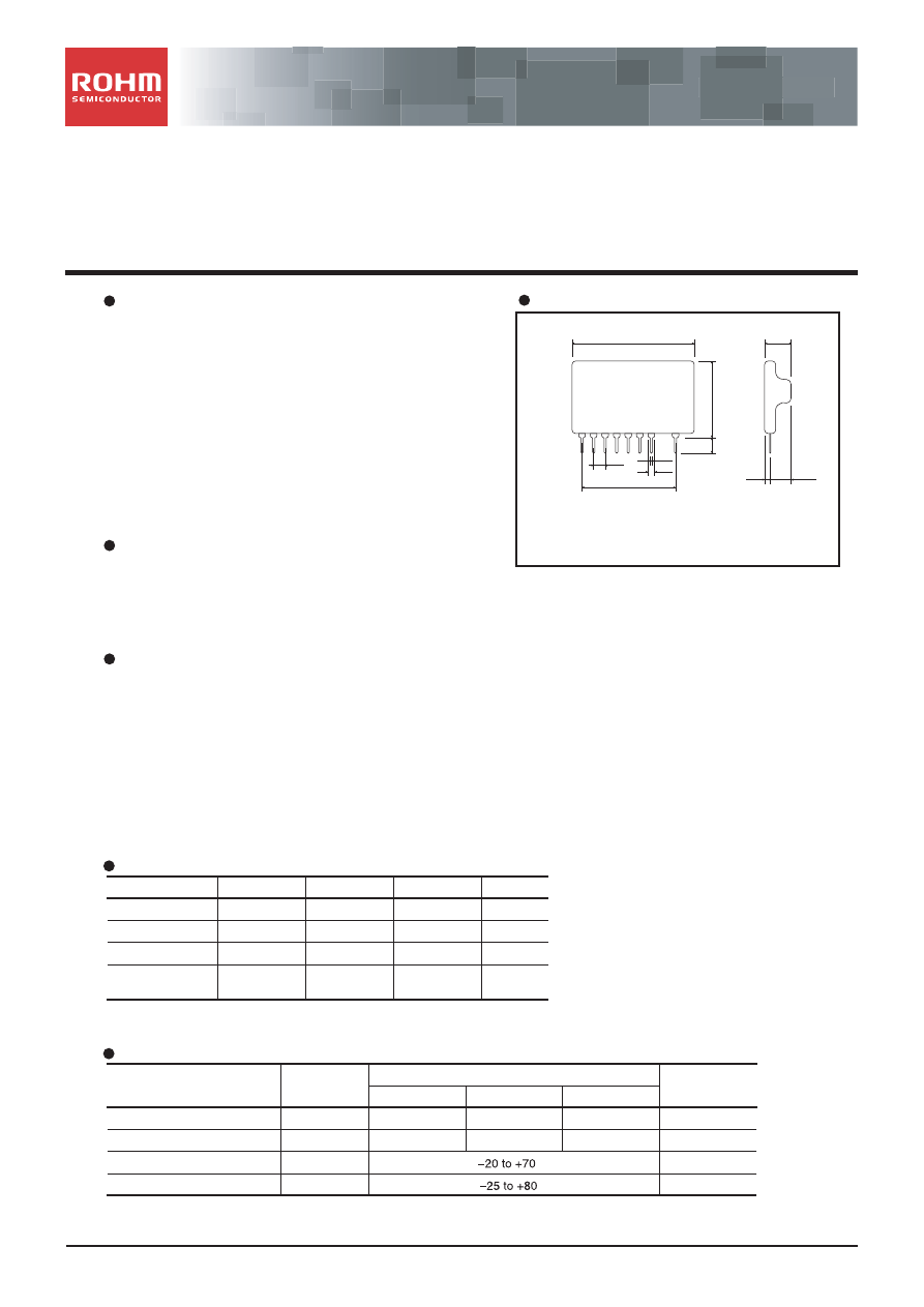
SIP9

1

28.0 Max.

19.5 Max.

4±1

Pin No.

2.54

0.5

1.4

2.54x

8=20.32

2

3

4

5

6 7

9

4.0

8.0

Max.

12.0
Max.

Max.

Marked side

Note : Dimensions without tolerance is typical.

Mar

k

ed side

Dimensions (Unit : mm)

1/7

2011.10 - 

Rev. C

www.rohm.com

© 2011  ROHM Co., Ltd. All rights reserved.

Data Sheet

bp5220a-html.html
background image

Data Sheet

BP5220A/BP5221A/BP5222A

DRIVE CIRCUIT

CONTROL CIRCUIT

POWER
SUPPLY
CIRCUIT

Vi

9

7

6

5

4

3

2

1

ADJ

CTL

GND

V

OUT

FB

BP5220A / BP5221A / BP5222A

N. C.

N. C.

N. C.

Parameter

Symbol

Unit

Conditions

Min.

Typ.

Max.

Input voltage

Vi

8

38

Output voltage

V

O

4.75

5

5.25

Output current

I

O

1

Line regulation

27

80

Vi=8V to 38V

Vi=8V to 38V

Load regulation

13

80

Io=0.1A to 1A

Io=0.05A to 0.5A

Output ripple voltage

22

70

Power conversion efficiency

75

85

Io=1A

Io=1A

Switching frequency

f

SW

190

CTL pin ON resistance

R

ON

4.7

Vo>4.75V

Vo>4.75V

CTL pin OFF resistance

Input voltage

Output voltage

Output current

Line regulation

Load regulation

Output ripple voltage

Power conversion efficiency

Switching frequency

CTL pin ON resistance

CTL pin OFF resistance

R

OFF

200

Vo<0.1V, SW=2

Vo<0.1V, SW=2

Symbol

Vi

V

O

I

O

f

SW

R

ON

R

OFF

Vi<30V

BP5221A 

(Unless otherwise noted : Vi=15V, Io=0.25A, SW=1, Ta=25˚C) 

Parameter

Unit

Conditions

Min.

Typ.

Max.

8

38

V

4.75

5

5.25

V

0.5

A

13

50

mV

3

50

mV

25

70

mV

PP

70

84

%

190

kHz

4.7

200

V

V

A

mV

mV

mV

PP

%

kHz

BP5220A 

(Unless otherwise noted : Vi=15V, Io=0.5A, SW=1, Ta=25˚C) 

Block diagram

Electrical characteristics

2/7

2011.10 - 

Rev. C

www.rohm.com

© 2011  ROHM Co., Ltd. All rights reserved.

bp5220a-html.html
background image

Data Sheet

BP5220A/BP5221A/BP5222A

BP5222A 

(Unless otherwise noted : Vi=20V, Io=0.25A, SW=1, Ta=25˚C) 

T

Output ripple voltage

Please note that output ripple voltage depends on the type and characteristics of the output capacitor.

Switching frequency=1/T

Fig.1

+

+

9

7

6

5

4

3

2

1

Input

A

V

V

A

f

SW

1

2

Output

4.7k

200k

BP5220A / BP5221A / BP5222A

f ; Frequency counter

Vi=15V to 38V

Io=0.05A to 0.5A

Io=0.5A

Vo>11.2V

Input voltage

Output voltage

Output current

Line regulation

Load regulation

Output ripple voltage

Power conversion efficiency

Switching frequency

CTL pin ON resistance

CTL pin OFF resistance

Vo<0.1V, SW=2

Symbol

Vi

V

O

I

O

f

SW

R

ON

R

OFF

Parameter

Unit

Conditions

Min.

Typ.

Max.

15

38

V

11.2

12

12.8

V

0.5

A

22

50

mV

18

50

mV

29

70

mV

PP

75

90

%

190

kHz

4.7

200

Measurement circuit

3/7

2011.10 - 

Rev. C

www.rohm.com

© 2011  ROHM Co., Ltd. All rights reserved.

bp5220a-html.html
background image

Data Sheet

BP5220A/BP5221A/BP5222A

Circuit operation

(1) The basic application examples are shown in Fig.2.
      The only external parts required are the input and
      output smoothing capacitors.

(2) Switching on and off the output voltage is allowed.
      The output can be switched off by making pin 4
      open (high impedance). (See Fig.3)

(3) Fine adjustment of the output voltage is allowed.
     Adjustment of the output voltage can be
     performed from pin 6 via the resistor by connecting
     the output terminal (pin 2) or GND. (See
     application example 3)

Application Examples

Application Example 1 : DC / DC converter with protection circuit

Fig.3

120pF

COMP.

+

BA10393

Vi

24V

V

O

5V

9

7 6 5 4 3 2 1

BP5220A / BP5221A / BP5222A

+

+

Fig.4

Vi

=

24V

0.2

0.4

0.6

0.8

1.0

1.2

6

5

4

3

2

1

0

OUTPUT CURRENT (A)

OUTPUT V

OL

TA

GE 

(V)

Fig.5

Fig.6

A resistor is used to limit the rise of output at power on. The resistance depends on the input voltage.
This is a standard application. Because the control current fluctuates with variations in circuits and components,
set the control current by adding a sufficient margin to the normal current level.

9

7

6

5

4

3

2

1

Vi

V

O

BP5220A / BP5221A / BP5222A

+

+

Fig.2

Be sure to use fuse for safety.

9

7

6

5

4

3

2

1

Vi

SW

V

O

BP5220A / BP5221A / BP5222A

Output OFF

+

+

Be sure to use fuse for safety.

Application Example 2 : Output ON / OFF control

9

7

6

5

4

3

2

1

Vi

V

O

470 F

100k

100k

2SC1740

BP5220A / BP5221A / BP5222A

ON / OFF

100 F

+

+

Be sure to use fuse for safety.

4/7

2011.10 - 

Rev. C

www.rohm.com

© 2011  ROHM Co., Ltd. All rights reserved.

bp5220a-html.html
background image

Data Sheet

BP5220A/BP5221A/BP5222A

Application Example 3 : Output voltage adjustment

(1) When reducing the output voltage

VR value setting equations (The output voltage after adjustment is denoted by Vo.)

(1) When reducing the output voltage

BP5220A / BP5221A
BP5222A

(2) When increasing the output voltage

BP5220A / BP5221A
BP5222A
To maximize performance we recommended the output voltage be
adjusted within ±20% of the output voltage rating. When the output voltage is increased by 20%, for
instance, the minimum input voltage is also increased by 20%.
(Example : When the output voltage is changed from 5V to 6V in the BP5220A, the minimum input voltage
is charged from 8V to 9.6V)

(2) When increasing the output voltage

Fig.7

Fig.9

Application Example 4 : Slow start
The slow start circuit mitigates the pulse load on the internal switching transistor when input voltage is applied,
and increases the output voltage gradually by starting the switching operation slowly.
This application is useful for preventing malfunction of an external protection circuit due to rush current,
and can serve as a countermeasure against operation outside the safe operation range. 

C1 is a slow-start capacitor for mitigating excessive rush current that flows into the module when the switch is
turned on. 

Vi

9

7

6

5

4

3

2

1

VR

BP5220A / BP5221A / BP5222A

V

O

+

+

Be sure to use
fuse for safety.

9

7

6

5

4

3

2

1

470 F

VR

V

O

BP5220A / BP5221A / BP5222A

+

Fig.8

100 F

Vi

+

Be sure to use
fuse for safety.

9

7

6

5

4

3

2

1

V

O

470 F

100k

C1

10 F

Vi

24V

470k

BP5220A / BP5221A / BP5222A

2SC1740R

100 F

+

+

+

Be sure to use
fuse for safety.

5/7

2011.10 - 

Rev. C

www.rohm.com

© 2011  ROHM Co., Ltd. All rights reserved.

bp5220a-html.html
background image

Data Sheet

BP5220A/BP5221A/BP5222A

(1) No circuit is installed in the modules to protect against excessive output currents. Therefore, take physical 
     safety measures such as using a fuse if short-circuit loading is probable.
(2) The output current should be reduced according to an increase in the input voltage or ambient temperature.
     Use the modules within the derating curve range.
(3) A large rush current may flow in the module when the input voltage is applied or the output ON / OFF is
      controlled with pin 4 without a capacitor such as C1 in application 4. Operating within the safe operation
      ranges shown in Fig.12, 15, and 18. 
      The safe operation range is determined by the safe operation range of the internal switching transistor.
      The amount of rush current depends on the output impedance of the input power supply and capacitors
      connected to the module outputs. The pulse load on the internal switching transistor at the start of operation
      can be reduced by using the protection circuit in application 1 or the slow start circuit in application 4.
(4) Pins 5 and 7 are not connected.
(5) A smoothing electrolytic capacitor is necessary for I/O external components. Please use a capacitor equivalent
      to the recommended one.
(6) Please put an I/O smoothing capacitor near the module. Output ripple voltage may be larger or output voltage
      may not be stable. 

BP5220A

BP5221A

0

25

50

70

1000

800

600

400

200

OUTPUT CURRENT :

 I

O

 (mA)

AMBIENT TEMPERATURE : Ta(

°

C)

100

120

0

25

50

70

100

120

1200

Vi=8 to 15V

Vi=34V

Vi=38V

Vi=25V

Vi=30V

Fig.10 Derating curve

OUTPUT CURRENT :

 I

O

 (mA)

AMBIENT TEMPERATURE : Ta(

°

C)

Fig.13 Derating curve

100

80

60

40

20

0

200

400

600

800

1000

OUTPUT CURRENT : I

O

 (mA)

Vi=8V

Vi=23V

Vi=38V

Fig.11 Efficiency

OUTPUT CURRENT : I

O

 (A)

Fig.14 Efficiency

20

10

5

3

2

1

0.5

0.3

0.2

0.1

1

2

3

5

10

20 30

50

Pw=0.2ms

Pw=1ms

VOLTAGE BETWEEN PIN2 AND PIN9 (V)

OUTPUT CURRENT INT

O PIN9 (A)

Tc=25

°

C

SINGLE PULSE

Fig.12 Safety operation range

VOLTAGE BETWEEN PIN2 AND PIN9 (V)

OUTPUT CURRENT INT

O PIN9 (A)

Fig.15 Safety operation range

0.5

0.4

0.3

0.2

0.1

Vi=30 to 38V

Vi=8 to 15V

0.6

100

80

60

40

20

0

0.1

0.2

0.3

0.4

0.5

Vi=8V

Vi=23V

Vi=38V

10

4.5A

2.2A

1

0.1

1

10

100

Pw=1ms

Pw=10ms

Operation notes

Electrical Characteristics Curves

Tc=25

°

C

SINGLE PULSE

6/7

2011.10 - 

Rev. C

www.rohm.com

© 2011  ROHM Co., Ltd. All rights reserved.

bp5220a-html.html
background image

Data Sheet

BP5220A/BP5221A/BP5222A

BP5222A

0

25

50

70

0.5

0.4

0.3

0.2

0.1

100

120

0.6

Vi=15 to 20V

Vi=30V

Vi=38V

Fig.16 Derating curve

100

80

60

40

20

0

0.1

0.2

0.3

0.4

0.5

Vi=30V

Vi=23V

Vi=38V

Fig.17 Efficiency

+

9

7

+

6

5

4

3

2

1

BP5220A / BP5221A / BP5222A

Pin 9 sink current

Voltage difference

between pins 2 and 9

Fig.19 ASO measurement circuit

Fig.18 Safety operation range

4.5A

10

2.2A

1

0.1

1

10

100

Pw=1ms

Pw=10ms

Tc=25

°

C

SINGLE PULSE

VOLTAGE BETWEEN PIN2 AND PIN9 (V)

OUTPUT CURRENT INT

O PIN9 (A)

OUTPUT CURRENT : I

O

 (A)

OUTPUT CURRENT :

 I

O

 (mA)

AMBIENT TEMPERATURE : Ta(

°

C)

7/7

2011.10 - 

Rev. C

www.rohm.com

© 2011  ROHM Co., Ltd. All rights reserved.

bp5220a-html.html
background image