39
Cal-Chip
EElleeccttrro
on
niiccss,, IIn
ncco
orrp
po
orraatteed
d
Stacked PEN Film Chip Capacitors - Standard
Stacked metalized PEN film as dielectric with simple mold-less construction
F
EATURES
• Small in size (minimum size 3.2 x 1.6mm)
• 85°C, 85% RH, W.V. x 1.0 for 500 hours
• Applicable for reflow soldering
R
ECOMMENDED
A
PPLICATIONS
• Coupling
• By-pass
• General Purpose
E
XPLANATION OF
P
ART
N
UMBERS
S
PECIFICATIONS
C
C
W
U
J
B
1
2
3
4
5
6
7
8
9
10
11
12
Product Code
Dielectric &
Construction
Rated Voltage
1C = 16 VDC
1H = 50 VDC
1 = 100 VDC
Nominal Capacitance
Cap.
Tolerance
Suffix
Suffix
Tape
Width
5 = 8 mm
9 = 12mm
Operating Temperature Range
Rated Voltage
Capacitance Range
Capacitance Tolerance
Withstand Voltage
Dissipation Factor
Insulation Resistance
Soldering Conditions
-55 to +105°C
16 VDC, 50 VDC, 100 VDC
0.001 to 0.47µF
±5% (J)
Between terminals: Rated voltage (VDC) x 175% 1 to 5 s
≤
1.0% (20°C, 1kHz)
16 VDC:
≥
3000 M
Ω
(20°C, 10VDC 60 s)
50 VDC:
≥
3000 M
Ω
(20°C, 50VDC 60 s)
100 VDC:
≥
3000M
Ω
(20°C, 100 VDC 60 s)
16 VDC: 1000M
Ω
• µF min. (20°C, 10 VDC 60 s)
Reflow soldering: 240°C max. and 30 sec max. at more than 210°C
(Temperature at capacitor surface)
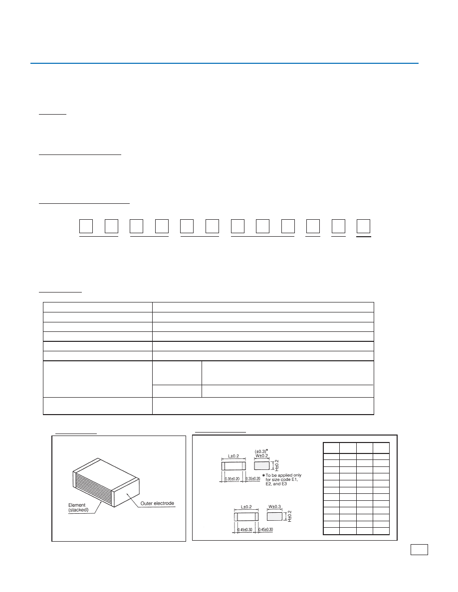
C
ONSTRUCTION
D
IMENSIONS IN MM
(not to scale)
C
≤
0.33µF
C>0.33µF
CCWU S
ERIES
Size
Code
H1
H2
H3
G1
G2
G3
E1
E2
E3
D1
D2
D3
L
3.2
3.2
3.2
3.2
3.2
3.2
4.8
4.8
4.8
6.0
6.0
6.0
W
1.6
1.6
1.6
2.5
2.5
2.5
3.3
3.3
3.3
4.1
4.1
4.1
H
0.8
1.0
1.4
1.0
1.4
2.0
1.4
2.0
2.8
1.8
2.0
2.4
• Size Code H1, H2, H3, G1, G2, G3, E1, E2, and E3
• Size Code D1, D2, and D3