background image

Rev 1.1 (May 2014)                                                      1                                           

©

 2013 DLP Design, Inc.  


D

D

L

L

P

P

-

-

R

R

F

F

4

4

3

3

0

0

B

B

P

P


B

B

o

o

o

o

s

s

t

t

e

e

r

r

P

P

a

a

c

c

k

k


U

U

s

s

e

e

r

r

s

s


G

G

u

u

i

i

d

d

e


FEATURES: 


Texas Instruments RF430CL330H, Rev D Silicon 


ISO14443B Compliant  


13.56MHz RF Interface Supports up to 848 Kbps 


NFC Tag Type 4 Compliant 


3K SRAM Bytes Available for NDEF Message Storage  


Automatic Checking of NDEF Structure 


Interrupt to Indicate End of Read or End of Write  


Onboard Antenna or Optional External Antenna Connection (Remove R2 and R3)  


Operational Power Supplied by the LaunchPad (Purchased Separately) 
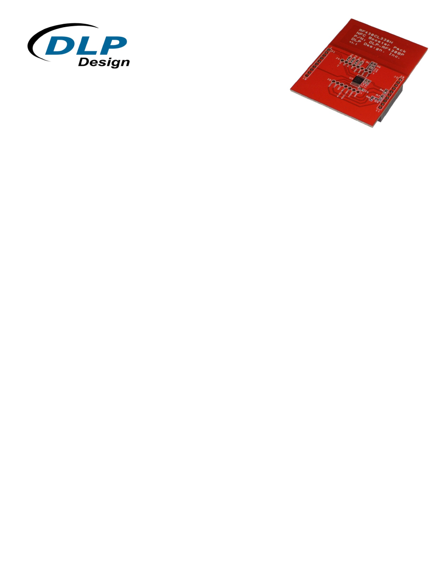


1.0   INTRODUCTION 


The DLP Design DLP-RF430BP BoosterPack is used to demonstrate the capabilities of the 
RF430CL330H and help aid in the development process by providing a working hardware/firmware 
reference example for NFC operations.  This BoosterPack demonstrates a secure, simplified pairing 
process for Bluetooth

®

 and Wi-Fi connections with the only dynamic NFC tag device designed 

specifically for NFC connection handover and service-interface functions. 
 
The DLP-RF430BP BoosterPack is an add-on board designed to fit TI’s MCU LaunchPads.  This product 
allows the software application developer to get familiar with the functionalities of the RF430CL330H on 
their Texas Instruments embedded microcontroller platform of choice without having to worry about 
designing the antenna. 
 
This document provides direction for RF430CL330H users who wish to implement an NFC tag emulator 
that is connected to and controlled by a Texas Instruments embedded microcontroller or microprocessor 
development platform.  Examples of such development platforms are the MSP-EXP430G2 LaunchPad 
and the MSP-EXP430F5529LP LaunchPad. 

LaunchPads from Texas Instruments are easy-to-use flash programming and debugging tools for the 
MSP430, C2000, TIVA, etc. lines of microcontrollers.  They feature everything you need to start 
developing on a Texas Instruments microcontroller device.  There is on-board emulation for 
programming and debugging, on-board button switches, LED’s and BoosterPack-compatible pinouts to 
support a wide range of plug-in modules like the DLP-RF430BP. 

Free software development tools are also available, such as TI’s Eclipse-based Code Composer Studio. 
Open-source development is also possible thanks to community-driven projects such as the MSPGCC 
compiler or Energia, a branch of the popular Wiring framework. 


dlp-rf430bp-ds-v11-html.html
background image

Rev 1.1 (May 2014)                                                      2                                           

©

 2013 DLP Design, Inc.  

2.0  SCOPE 


This document describes the DLP-RF430BP module for evaluation and development purposes in 
conjunction with Texas Instruments embedded development platforms.  This manual does not cover the 
in-depth details of the 

RF430CL330H

 family as these are documented in the datasheets for those parts 

along with application notes that can be found on their product pages (see the links in Section 3). 


3.0  REFERENCES 


•  DLP-RF430BP:  

www.tiboosterpacks.com

 or 

www.dlpdesign.com


•  RF430CL330H Product Page:  

http://www.ti.com/product/rf430cl330h


•  RF430CL330H Datasheet:  

http://www.ti.com/lit/ds/symlink/rf430cl330h.pdf


4.0  MODULE DESCRIPTION 


The DLP-RF430BP BoosterPack (Figure 1) allows NFC connection handover for an alternative carrier 
like Low Energy (BLE) and Wi-Fi as an easy and intuitive pairing or authentication process with only a 
tap.  As a general NFC interface, the RF430CL330H enables electronic products to communicate with 
the fast-growing infrastructure of NFC-enabled smart phones, tablets and notebooks. 
 
Connection to Texas Instruments LaunchPad platforms are made via 10-pin, 0.1-inch spaced,  
0.025-square inch female headers located on the back of the board.  The electrical schematic is 
available for download from both the DLPDesign.com and TIBoosterPacks.com sites. 


Figure 1.  DLP-RF430BP Evaluation Module


dlp-rf430bp-ds-v11-html.html
background image

Rev 1.1 (May 2014)                                                      3                                           

©

 2013 DLP Design, Inc.  

5.0  MODULE PINOUT 


DLP-RF430BP MODULE PIN CONNECTIONS TO THE LAUNCHPAD 

VCC - 3.0V power from the LaunchPad 

Unused by the DLP-RF430BP 

Unused by the DLP-RF430BP 

Unused by the DLP-RF430BP 

Unused by the DLP-RF430BP 

Unused by the DLP-RF430BP 

DATA_CLK - Clock from the microcontroller if in SPI mode.  Default: I2C mode.  

RESET  

Unused by the DLP-RF430BP 

10 

Unused by the DLP-RF430BP 

11 

Unused by the DLP-RF430BP 

12 

INTO - Interrupt to microcontroller 

13 

SPI_CS - Chip select from microcontroller for SPI mode 

14 

MISO/SCL - SPI serial data to the microcontroller if in SPI mode. Clock from 
microcontroller if in I2C mode. 

15 

MOSI/SDA - SPI serial data from the microcontroller if in SPI mode.  Data to/from 
microcontroller if in I2C mode. 

16 

Unused by the DLP-RF430BP 

17 

Unused by the DLP-RF430BP 

18 

Unused by the DLP-RF430BP 

19 

Unused by the DLP-RF430BP 

20 

GROUND 


6.0  QUICK START GUIDE 


If using Code Composer to load, edit and compile the demonstration firmware: 
 
1. Remove jumper P1.6 from the G2 LaunchPad.  
 
2. Attach the G2 LaunchPad to the DLP-RF430BP as shown here. 


3.  Apply power by connecting a USB cable to the LaunchPad. 

4.  Load (Import) the base application firmware into Code Composer Studio.  The firmware project is 
available for download from this link:  http://www.ti.com/lit/zip/sloc303


5.  Enter Debug mode and test for basic functionality by holding an NFC-enabled smart phone, tablet or 
notebook close to the onboard loop antenna.  The device should display "Hello, world!" for the default 
NDEF message.


dlp-rf430bp-ds-v11-html.html
background image

Rev 1.1 (May 2014)                                                      4                                           

©

 2013 DLP Design, Inc.  

6.  Modify the source code as desired to change the default message. 


If using Uniflash to load the precompiled .out file: 
 
1. Remove jumper P1.6 from the G2 LaunchPad. 
 
2. Attach the G2 LaunchPad to the DLP-RF430BP as shown here. 


3.  Apply power by connecting a USB cable to the LaunchPad. 

4. Download Uniflash - http://www.ti.com/tool/uniflash 

5. Make a new target configuration for the MSP430G2553:  Click on File, New Target Configuration, 
which leads you to this window to launch the session:  


dlp-rf430bp-ds-v11-html.html
background image

Rev 1.1 (May 2014)                                                      5                                           

©

 2013 DLP Design, Inc.  

6. Next, click on Program, Load Program, and navigate (using Browse button) to the project files and find 
the .out file 


7. Click OK to load the .out file.   

8. Cycle power on the LauchPad (unplug - replug) and the code will be running.  

9. Test for basic functionality by holding an NFC-enabled smart phone, tablet or notebook close to the 
onboard loop antenna.  The device should display "Hello, world!" for the default NDEF message.


7.0  BASE APPLICATION FIRMWARE 


DLP-RF430BP Module Application Firmware for the various Texas Instruments LaunchPads is available 
from the DLP Design websites.  Visit the appropriate download/product pages for all available firmware 
project downloads. 


dlp-rf430bp-ds-v11-html.html
background image

Rev 1.1 (May 2014)                                                      6                                           

©

 2013 DLP Design, Inc.  

8.0  MECHANICAL DIMENSIONS – Inches (mm) 


RF430

2.60 typ

(66.0 typ)

2.0  typ

(50.8 typ)

Loop Antenna

1.8  typ

(45.7 typ)

1.0  typ

(25.4 typ)

1.13  typ

(28.7 typ)

0.34 typ

(8.6 typ)


9.0  DISCLAMER 


Neither the whole nor any part of the information contained herein nor the product described in this 
datasheet may be adapted or reproduced in any material or electronic form without the prior written 
consent of the copyright holder. 
 
This product and its documentation are supplied on an as-is basis, and no warranty as to their suitability 
for any particular purpose is either made or implied.  DLP Design will not accept any claim for damages 
whatsoever arising as a result of the use or failure of this product.  Your statutory rights are not affected. 
 
This product or any variant of it is not intended for use in any medical appliance, device or system in 
which the failure of the product might reasonably be expected to result in personal injury. 
 
This document provides preliminary information that may be subject to change without notice. 


10.0  CONTACT INFORMATION 


DLP Design, Inc. 
1605 Roma Lane 
Allen, TX  75013 
 
Phone: 469-964-8027 
Fax: 415-901-4859 
Email: support@dlpdesign.com 
Internet:      http://www.dlpdesign.com


dlp-rf430bp-ds-v11-html.html
background image

5

5

4

4

3

3

2

2

1

1

D

D

C

C

B

B

A

A

VCC (+3.3V)

Analog In

UART_RX

UART_TX

GPIO (INT)

SPI_A_CLK

SPI_B_CLK

GPIO

GPIO

GPIO

LAUNCH PAD PIN DEFINITION

RESET

Timer Output

SPI_B_SIMO/I2C_SDA

SPI_B_SOMI/I2C_SCL

GPIO

GPIO

GND

GPIO (INT)

TEST

GPIO

NOTE:

/CS=1 AT POWER UP SELECTS SPI

/CS=0 AT POWER UP SELECTS I2C

NOTE:

/RST HAS INTERNAL PULLUP

/CS HAS INTERNAL PULLUP

DEFAULT COM CONFIGURATION IS I2C.

TO USE SPI REMOVE R8 AND PUT 0

OHM IN R9.

DLP-RF430BP

1.0

DLP-RF430BP : RF430CL330H Booster Pack

A

01

Saturday, November 16, 2013

Title

S

iz

e

Document Number

Rev

Date:

Sheet

of

SCK

/RESET

SCK

INTO

INTO

MISO/SCL

MOSI/SDA

/RESET

MOSI/SDA

MISO/SCL

/SPI_CS

/SPI_CS

VCORE

VCORE

MOSI/SDA

MISO/SCL

SCK

/CS

/CS

INTO

AN

T2

ANT

1

E0

E1

E2

E0

ANT

1

E2

/RESET

E1

ANT

2

VIN_3.3V

VIN_3.3V

VIN_3.3V

VIN_3.3V

J1

HEADER A

1

2

3

4

5

6

7

8

9

10

R3

0

C4

0.1uF

R8

0

C6

0.47uF

C1

0.1uF

J2

HEADER B

20

19

18

17

16

15

14

13

12

11

R9

DNS

J5

DNS

1

2

3

4

5

6

7

C2

12pF

R7

4.7K

R4

0

U1

RF430CL330H

1

2

3

4

5

6

7

14

13

12

11

10

9

8

VCC

ANT1

ANT2

RST

E0

E1

E2

VSS

VCORE

MOSI/SDA

MISO/SCL

SCK

CS

INTO

R1

0

C5

1uF

J4

DNS

1

2

3

4

5

6

7

8

C3

DNS

R5

0

R6

4.7K

R2

0