I N T E G R AT I O N
Flash FPGAs
Flash SoC FPGAs
Military FPGAs
Automotive FPGAs
Design Tools
Development Kits
Solutions
Intellectual Property
FPGA and SoC Product Catalog
Lowest Power, Proven Security, and Exceptional Reliability
I N T E G R AT I O N
Flash FPGAs
Flash SoC FPGAs
Military FPGAs
Automotive FPGAs
Design Tools
Development Kits
Solutions
Intellectual Property
FPGA and SoC Product Catalog
Lowest Power, Proven Security, and Exceptional Reliability
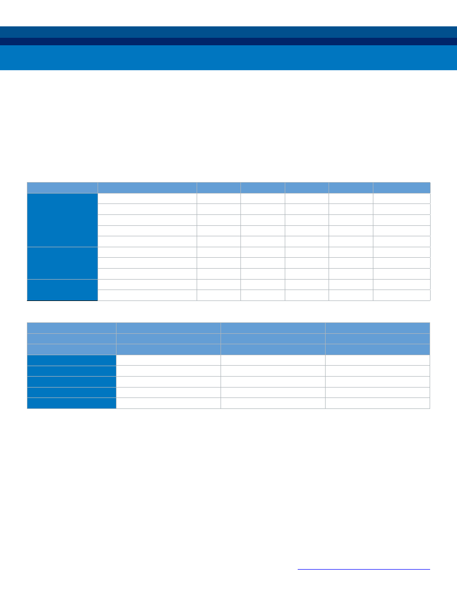
2
Features
SmartFusion
ProASIC3, IGLOO
SmartFusion2
IGLOO2
PolarFire
Logic Elements
100 - 30K
5K - 150K
100K - 480K
Transceiver Rate
--
1-5 Gbps
250 Mbps-12.7 Gbps
I/O Speeds
400 Mbps LVDS
667 Mbps DDR3
750 Mbps LVDS
1600 Mbps DDR4
1.6 Gbps LVDS
DSP (18x18 Multipliers)
--
240
1480
Max RAM
144 Kb
5 Mb
33 Mb
Processor Option
Hard 100 MHz
ARM Cortex-M3
Hard 166 MHz
ARM Cortex-M3
Soft RISC-V
Soft RISC-V
Soft ARM Cortex-M1
Hard Crypto Processor
On-board Flash
Up to 512 KB code store
Up To 512 KB code store
56 KB secure NVM
Family Type
CPLD Replacements
Smallest Packages
Low Density FPGAs with more resources
and lowest power
Mid-Range Density FPGAs
Lowest Power, Cost Optimized
Broad Range FPGA Supplier (1-500K LE)
3
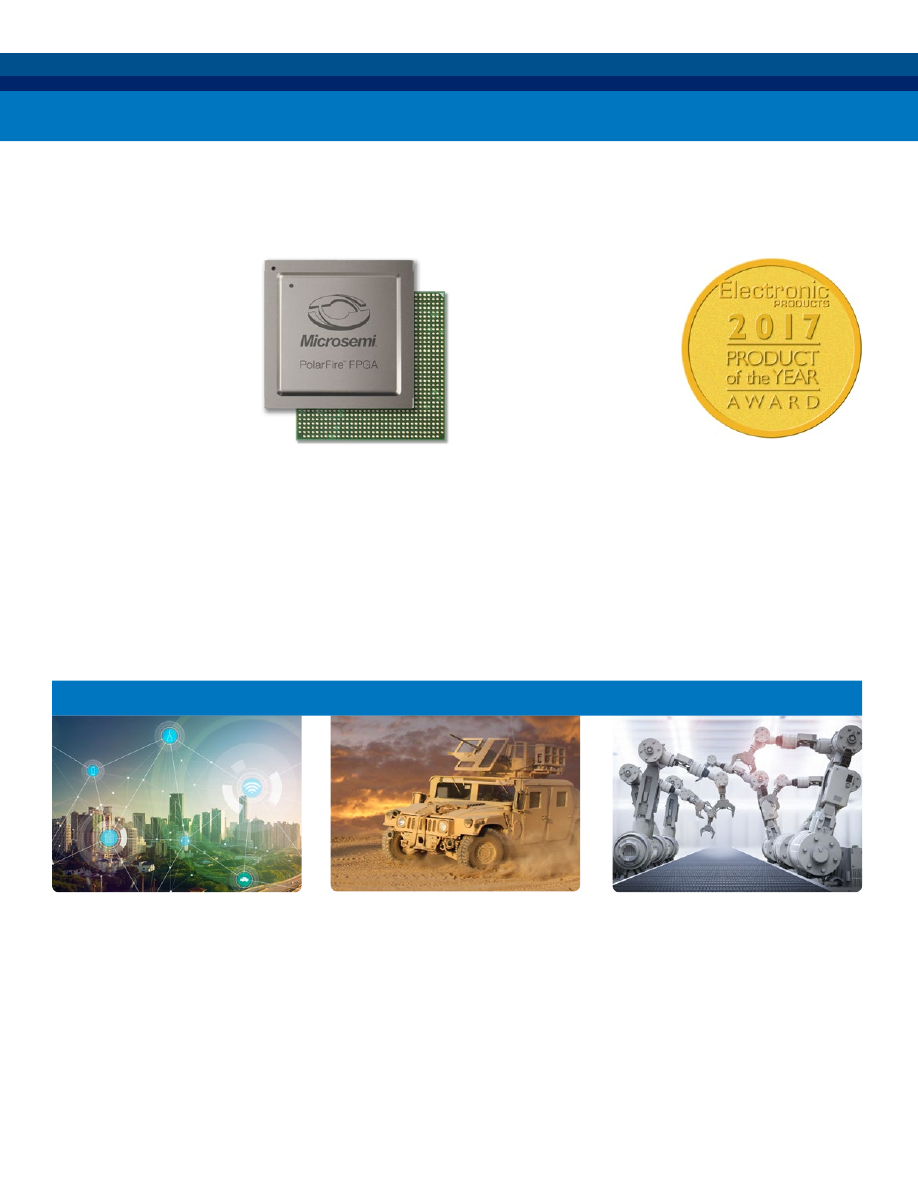
PolarFire FPGA
• Award winning cost optimized, lowest power
mid-range density FPGA
• 100K to 500K LEs
• Transceivers up to 12.7 Gbps
4
SmartFusion
®
2 SoC FPGA
• 166 MHz ARM
®
Cortex
®
-M3 processor
• 5K to 150K logic elements
• PCIe Gen2 hard IP and complete microcontroller
subsystem
7
IGLOO
®
2 FPGA
• The most feature-rich low-density FPGA
• 5K to 150K logic elements
• High-performance memory subsystem
8
IGLOO FPGA
• 100 to 35K logic elements
• Ideal for CPLD replacement
• Smallest package options
• High I/O-to-logic ratio
9
ProASIC
®
3 FPGA
• 100 to 35K logic elements
• Ideal for CPLD replacement
• Smallest package options
12
SmartFusion SoC FPGA
• 100 MHz ARM Cortex-M3 processor
• Up to 6K logic elements, analog processing
15
Military Products
• Military FPGA with up to 150K logic elements
• Best-in-class security
• Industry’s most reliable FPGAs
16
Automotive-Grade Products
• AEC-Q 100 T1 and T2 devices
• 1K to 90K logic elements
17
Design Tools
• Design software for Microsemi FPGAs and SoC FPGAs
18
Development Kits
• PolarFire based evaluation boards
• IGLOO2 & SmartFusion2 based kits
20
Imaging and Video Solutions
• FMC based evaluation boards & IP
24
Motor Control Solutions
• Complete solution including evaluation board, IP
and software
25
Intellectual Property Cores
• Microsemi intellectual property designed and optimized
for use with Microsemi FPGAs
26
Microsemi FPGAs and SoC FPGAs
For the latest device information, valid ordering codes, and details regarding previous generations of flash FPGAs,
visit www.microsemi.com/fpga-soc or consult the corresponding product datasheets.
Whether you’re designing at the board or system level, Microsemi’s SoC FPGAs and low-power FPGAs are your best choice.
The unique, flash-based technology of Microsemi FPGAs and their history of reliability sets them apart from traditional FPGAs.
Design with Microsemi’s FPGAs and SoC FPGAs for today’s rapidly-growing consumer and portable medical device markets, or
tomorrow’s environmentally friendly data centers, industrial controls, and military and commercial aircraft. Only Microsemi can meet
the power, size, cost, and reliability targets that reduce time-to-market and enable long-term profitability.
Product Highlights
4
Cost-optimized Architecture
• Transceiver performance optimized for 12.7 Gbps, which
yields smaller size
• Architecture and process optimizations for specific
bandwidths (10 Gbps–40 Gbps) at specific densities
• 1.6 Gbps I/Os—best-in-class hardened I/O gearing logic
with CDR (supports SGMII/GbE links on these GPIOs)
• High-performance, best-in-class hardened security IP in
mid-range devices
Industrial
• Increased networking of factory
automation
• M2M—growth of additional sensors
and nodes
• Rise of cloud services requiring
decentralized, secure computing
• Portability becoming more prevalent
• Cyber security threats
• Functional safety
Defense
• Anti-tamper for Foreign Military
Sales (FMS)
• Increasing automation in vehicles
and weaponry
• Enhancing operator situational
awareness
• Battlefield portability and increased
mission life
• Increased cybersecurity
• Supply chain security
Communications
• Significantly improved network
capacity and coverage with limited
spectrum and CAPEX
• Delivers 4K video
• Lower OPEX
• IoT growth with minimal energy
consumption
• Lower physical and carbon footprint
Power Optimization
• The lowest static power—28nm non-volatile process yields
very low static power
• Optimized for 12.7 Gbps, which yields the lowest power
• Low power modes—Flash*Freeze yields best-in-class
standby power
• Integrated hard IP—DDR PHY, PCIe endpoint/root port,
crypto processor
• Total power (static and dynamic)—up to 50% lower power
Solving Key Market Issues
PolarFire Cost-optimized FPGAs Deliver the Lowest Power at Mid-range Densities
Microsemi extends its non-volatile FPGA leadership with the
PolarFire family of cost-optimized FPGAs. PolarFire FPGAs deliver
up to 50% lower power than equivalent SRAM FPGAs. The
devices are ideal for a wide range
of applications within wireline
access networks and cellular
infrastructure, defense and
commercial aviation markets, as
well as industrial automation and
IoT markets.
As a true broad-range FPGA supplier, Microsemi offers FPGA
product families spanning 1K to 500K logic elements (LEs).
The devices offer unprecedented capabilities while
maintaining all the advantages
traditionally associated with non-
volatile FPGAs such as the lowest
static power, security, and single
event upset (SEU) immunity.
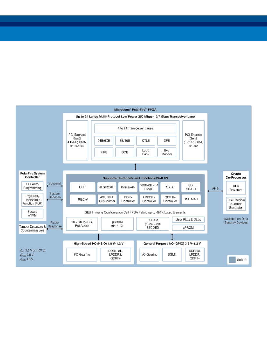
PolarFire FPGAs
5
Reliability Features
• SEU immune FPGA configuration cells
• Built-in SECDED and memory
interleaving on LSRAMs
• System controller suspend mode
for safety-critical designs
PolarFire FPGAs Deliver Up to 500K Logic Elements, 12.7G Transceivers at 50% Lower Power
• High-speed serial connectivity with
built-in multi-gigabit/multi-protocol
transceivers from 250 Mbps to 12.7 Gbps
• Up to 481K logic elements consisting
of a 4-input look-up table (LUT) with a
fractureable D-type flip-flop
• Up to 33 Mbits of RAM
• Up to 1480 18x18 multiply accumulate
blocks with hardened pre-adders
• Integrated dual PCIe for up to x4 Gen 2
endpoint (EP) and root port (RP) designs
• High-speed I/O (HSIO) supporting
up to 1600 Mbps DDR4, 1333 Mbps
DDR3L, and 1333 Mbps LPDDR3/DDR3
memories with integrated I/O gearing
• General purpose I/O (GPIO)
supporting 3.3 V built-in CDR to
support SGMII for serial gigabit
Ethernet, 1067 Mbps DDR3, and
1600 Mbps LVDS I/O speed with
integrated I/O gearing logic
Security Features
• Cryptography Research Incorporated
(CRI)-patented differential power
analysis (DPA) bitstream protection
• Integrated physically unclonable
function (PUF)
• 56 Kbytes of secure eNVM (sNVM)
• Built-in tamper detectors and
countermeasures
• Integrated Athena TeraFire EXP5200B
Crypto Co-processor, Suite
B-capable
• Digest integrity check for FPGA,
μPROM, and sNVM
• True random number generator
• CRI DPA countermeasure pass
through license
PolarFire Architecture
6
Security Advantage
Low Density
Mid-Range
Microsemi
Competition
Microsemi
Competition
Prevent overbuilding and cloning
Best
Low-density
Security
N/A
Best
Security
in the
Industry
N/A
Full design IP protection
N/A
Weak
Root of trust
N/A
N/A
Secure data communications
N/A
Weak
Anti-tamper
N/A
N/A
PolarFire FPGAs
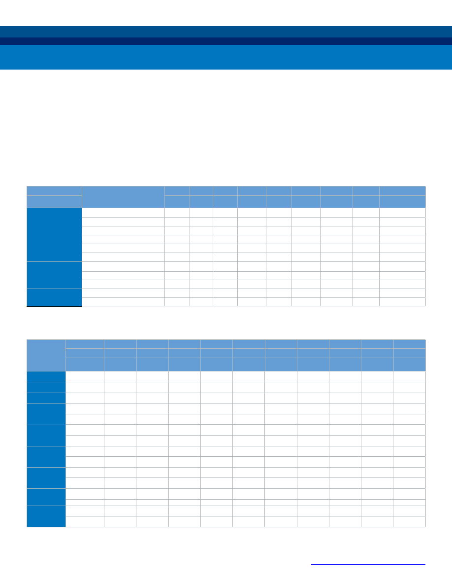
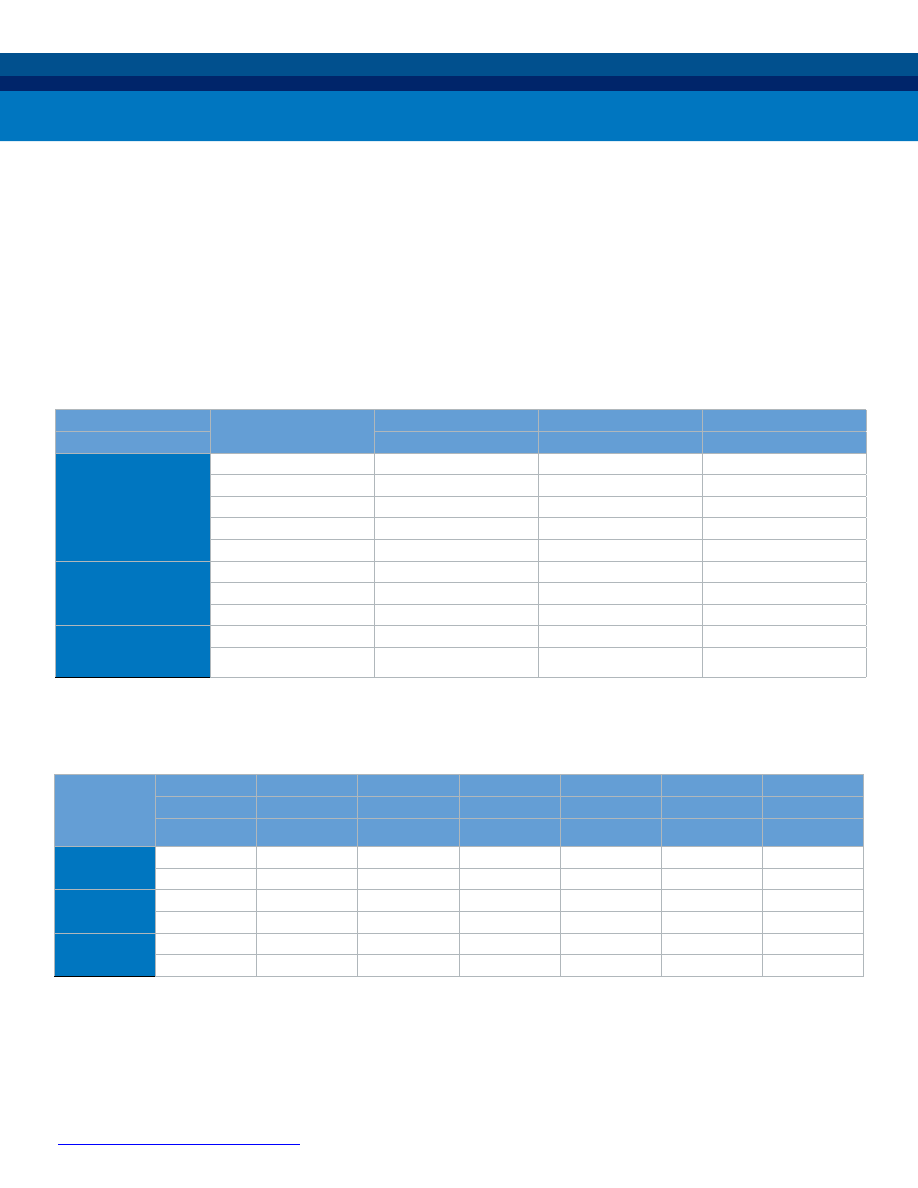
Features
MPF100T
MPF200T
MPF300T
MPF500T
FPGA
fabric
Logic elements (4 LUT + DFF)
109
192
300
481
Math blocks (18 x 18 MACC)
336
588
924
1480
LSRAM blocks (20 kbits)
352
616
952
1520
µSRAM blocks (64 x 12)
1008
1764
2772
4440
Total RAM (Mbits)
7.6
13.3
20.6
33
µPROM (Kbits, 9-bit bus)
297
297
459
513
User DLLs/PLLs
8
8
8
8
High-
speed I/O
250 Mbps to 12.7 Gbps transceiver lanes
8
16
16
24
PCIe Gen2 endpoints/root ports
2
2
2
2
Total I/Os
Total user I/Os
284
368
512
584
Packaging
Type/size/pitch
Total user I/Os (HSIO/GPIO)/transceivers
FCSG325
(11 mm x 11 mm, 11 mm x 14.5 mm*, 0.5 mm)
170(84/86)/4
170(84/86)/4*
FCSG536 (16 mm x 16 mm, 0.5 mm)
300(120/180)/4
300(120/180)/4
FCVG484 (19 mm x 19 mm, 0.8 mm)
284(120/164)/4
284(120/164)/4
284(120/164)/4
FCG484 (23 mm x 23 mm, 1.0 mm)
244(96/148)/8
244(96/148)/8
244(96/148)/8
FCG784 (29 mm x 29 mm, 1.0 mm)
368(132/236)/16 388(156/232)/16 388(156/232)/16
FCG1152 (35 mm x 35 mm, 1.0 mm)
512(276/236)/16 584(324/260)/24
Devices in the same package and family type are pin-compatible.
*Wider package dimension applies to the MPF200 device only.
“The number of IoT sensors is expected to approach 30 billion
in 5 years – and each unit is a potential entry point for cyber-
criminals” –
The Economist Intelligence Unit, 4/11/2016
“Some call cybercrime the greatest transfer of wealth in human
history” –
The Center of Strategic and International Studies,
July 2013, The Economic Impact of Cybercrime
Cyber Security is the #1 Concern for Connected Devices on the Network Edge
It is not enough for today’s demanding applications to meet the functional requirements of their design—they must do so in a
secured way. Security starts during silicon manufacturing and continues through system deployment and operations. Microsemi’s
PolarFire FPGAs represent the industry’s most advanced secure programmable FPGAs.
Feature and Packaging Overview of the PolarFire FPGA Family
Microsemi Security Leadership
PolarFire FPGAs
7
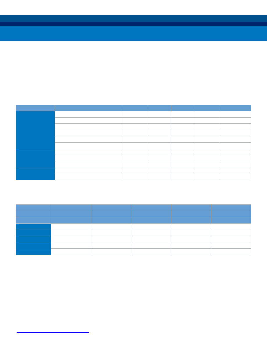
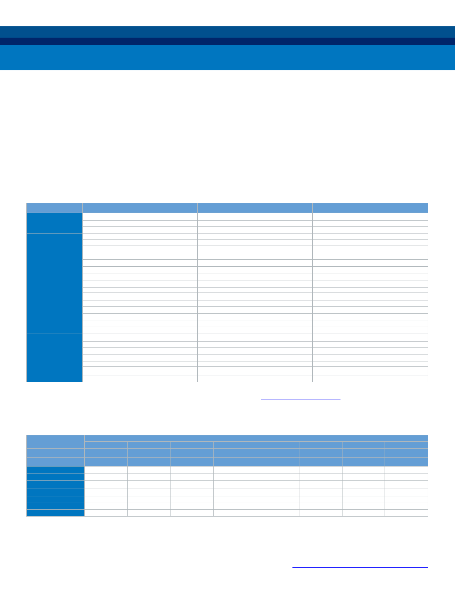
SmartFusion2 Devices
Features
M2S005
M2S010
M2S025
M2S050
M2S060
M2S090
M2S150
Logic/DSP
Maximum logic elements (4LUT + DFF)
6,060
12,084
27,696
56,340
56,520
86,184
146,124
Mathblocks (18 × 18)
11
22
34
72
72
84
240
Fabric interface controllers (FICs)
1
2
1
2
PLLs and CCCs
2
6
8
Security
AES256, SHA256, RNG
AES256, SHA256, RNG, ECC, PUF
MSS
Cortex-M3 + instruction cache
Yes
eNVM (KB)
128
256
512
eSRAM (KB)
64
eSRAM (KB) non-SECDED
80
CAN, 10/100/1000 Ethernet, HS USB
1 each
Multi-mode UART, SPI, I2C, timer
2 each
Fabric memory
LSRAM 18K blocks
10
21
31
69
109
236
uSRAM 1K blocks
11
22
34
72
112
240
Total RAM (kbits)
191
400
592
1,314
2,074
4,488
High-speed
DDR controllers (count × width)
1 × 18
2 × 36
1 × 18
2 x 36
SERDES lanes
0
4
8
4
16
PCIe endpoints
0
1
2
4
User I/O
MSIO (3.3 V)
115
123
157
139
271
309
292
MSIOD (2.5 V)
28
40
62
40
106
DDRIO (2.5 V)
66
70
176
76
176
Total user I/Os
209
233
267
377
387
425
574
Package Options
Package type
FCS(G)325
VF(G)256
FCS(G)536
VF(G)400
FCV(G)484
TQ(G)144
FG(G)484
FG(G)676
FG(G)896
FC(G)1152
Pitch (mm)
0.5
0.8
0.5
0.8
0.5
1.0
1.0
1.0
1.0
Length × width (mm)
11 × 11
14 × 14
16 × 16
17 × 17
19 × 19
20 × 20
23 × 23
27 × 27
31 × 31
35 × 35
Device
I/O Lanes I/O
Lanes
I/O Lanes I/O Lanes I/O
Lanes
I/O
Lanes
I/O Lanes I/O
Lanes
I/O
Lanes
I/O
Lanes
M2S005 (S)
161
171
84
209
M2S010 (S/T/TS)
138
2
195
4
84
233
4
M2S025 (T/TS)
180
2
138
2
207
4
267
4
M2S050 (T/TS)
200
2
207
4
267
4
377
8
M2S060 (T/TS)
200
2
207
4
267
4
387
4
M2S090 (T/TS)
180
4
267
4
425
4
M2S150 (T/TS)
293
4
248
4
574
16
www.microsemi.com/products/fpga-soc/soc-fpga/smartfusion2
Notes:
1. M2S090 FCSG325 package dimension are 11 × 13.5.
2. Highlighted devices can migrate vertically in the same package.
3. (G) indicates that the package is RoHS 6/6 compliant/Pb-free.
• Embedded ARM Cortex-M3
microcontroller subsystem (MSS)
• PCIe Gen2 endpoints starting at
10K logic elements
• Embedded DDR3 memory controllers
• Small packages
• 1 mW in Flash*Freeze mode
• Instant-on
• Zero FIT FPGA configuration cells
• SECDED memory protection
• NRBG, AES-256, SHA-256, ECC
cryptographic engine
• User physically unclonable function
(PUF)
• CRI DPA pass-through license
More Resources in Low-Density Devices with ARM Cortex-M3 Processor
SmartFusion2 SoC FPGAs deliver more resources in low-density devices with low power requirements, proven security, and
exceptional reliability. These devices are ideal for general purpose functions such as Gigabit Ethernet or dual-PCI Express control
planes, bridging functions, input/output (I/O) expansion and conversion, video/image processing, system management, and secure
connectivity. Microsemi SoC FPGAs are used by customers in Communications, Industrial, Medical, Defense, and Aviation markets.
SmartFusion2 Devices
I/Os per Package
S m a r t Fu s i o n 2 SoC FPGAs
8
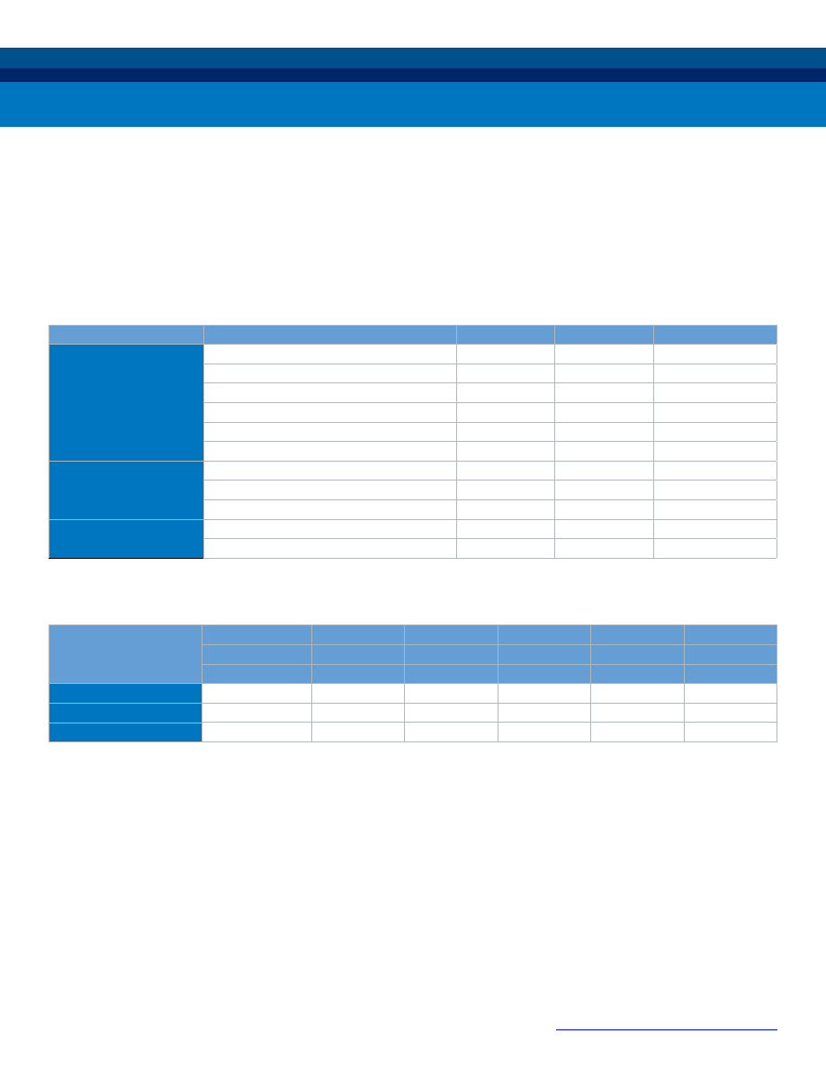
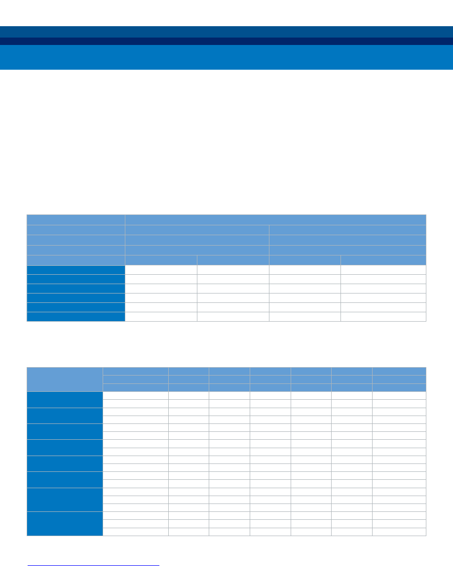
IGLOO2 Devices
Features
M2GL005 M2GL010 M2GL025 M2GL050 M2GL060 M2GL090
M2GL150
Logic/DSP
Maximum logic elements (4LUT + DFF)
6,060
12,084
27,696
56,340
56,520
86,184
146,124
Mathblocks (18 × 18)
11
22
34
72
72
84
240
PLLs and CCCs
2
6
8
SPI/HPDMA/PDMA
1 each
Fabric interface controllers (FICs)
1
2
1
2
Data security
AES256, SHA256, RNG
AES256, SHA256, RNG, ECC, PUF
Memory
eNVM (KB)
128
256
512
LSRAM 18K blocks
10
21
31
69
109
236
uSRAM 1K blocks
11
21
34
72
112
240
eSRAM (KB)
64
Total RAM (kbits)
703
912
1104
1826
2586
5000
High-speed
DDR controllers (count × width)
1 × 18
2 × 36
1 × 18
2 × 36
SERDES lanes
0
4
8
4
16
PCIe endpoints
0
1
2
4
User I/O
MSIO (3.3 V)
115
123
157
139
271
309
292
MSIOD (2.5 V)
28
40
62
40
106
DDRIO (2.5 V)
66
70
176
76
176
Total user I/Os
209
233
267
377
387
425
574
Grades
Commercial (C), Industrial (I), Military (M)
C, I
C, I, M
Package Options
Package type
FCS(G)325
VF(G)256
FCS(G)536
VF(G)400
FCV(G)484
TQ(G)144
FG(G)484
FG(G)676
FG(G)896
FC(G)1152
Pitch (mm)
0.5
0.8
0.5
0.8
0.5
1.0
1.0
1.0
1.0
Length × width (mm)
11x11
14x14
16x16
17x17
19x19
20x20
23x23
27x27
31x31
35x35
Device
I/O Lanes I/O Lanes I/O Lanes I/O Lanes I/O Lanes I/O
Lanes
I/O Lanes I/O
Lanes
I/O
Lanes
I/O
Lanes
M2GL005 (S)
161
171
84
209
M2GL010 (S/T/TS)
138
2
195
4
84
233
4
M2GL025 (T/TS)
180
2
138
2
207
4
267
4
M2GL050 (T/TS)
200
2
207
4
267
4
377
8
M2GL060 (T/TS)
200
2
207
4
267
4
387
4
M2GL090 (T/TS)
180
4
267
4
425
4
M2GL150 (T/TS)
293
4
248
4
574
16
www.microsemi.com/products/fpga-soc/fpga/igloo2-fpga
Notes:
1. Total logic may vary based on utilization of DSP and memories in your design. Please see the
IGLOO2 and SmartFusion2 Fabric User Guide
for details
.
2. Feature availability is package dependent.
Notes:
1. M2GL090 FCS325 package dimension are 11 x 13.5.
2. Highlighted devices can migrate vertically in the same package.
3. (G) indicates that the package is RoHS 6/6 compliant/Pb-free
• High-performance
memory subsystem
• PCIe Gen2 endpoints starting
at 10K logic elements
• Embedded DDR3 memory controllers
• SECDED memory protection
• 1 mW in Flash*Freeze mode
• Instant-on
• Zero FIT FPGA configuration cells
• CRI DPA pass-through license
• Small packages
• NRBG, AES-256, SHA-256,
ECC cryptographic engine
• User physically unclonable
function (PUF)
IGLOO2 Devices
I/Os per Package
More Resources in Low-Density Devices with High-Performance Memory Subsystem
IGLOO2 FPGAs deliver more resources in low-density devices with low power requirements, proven security, and exceptional
reliability. These devices are ideal for general purpose functions such as Gigabit Ethernet or dual-PCI Express control planes,
bridging functions, input/output (I/O) expansion and conversion, video/image processing, system management, and secure
connectivity. Microsemi FPGAs are used by customers in Communications, Industrial, Medical, Defense, and Aviation markets.
I G L O O 2 FPGAs
9
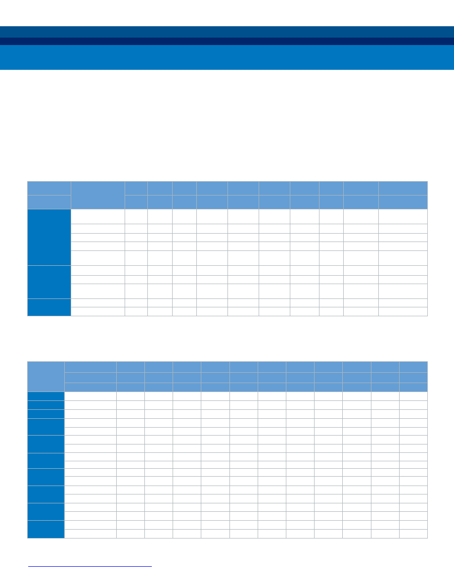
IGLOO devices
Features
AGL030 AGL060 AGL125
AGL250
AGL400
AGL600
AGL1000
AGLE600
AGLE3000
ARM-Enabled
IGLOO
1
devices
M1AGL250
M1AGL600 M1AGL1000
M1AGLE3000
Logic
Logic elements (approximate)
330
700
1,500
3,000
5,000
7,000
11,000
7,000
35,000
System gates
30,000
60,000
125,000
250,000
400,000
600,000
1,000,000
600,000
3,000,000
VersaNet globals
3
6
18
18
18
18
18
18
18
18
Flash*Freeze mode (typical, μW)
5
10
16
24
32
36
53
49
137
AES-protected ISP
1
Yes
Yes
Yes
Yes
Yes
Yes
Yes
Yes
Integrated PLLs with CCC
2
1
1
1
1
1
1
6
6
Fabric memory
RAM (1,024 bits)
18
36
36
54
108
144
108
504
RAM blocks (4,608 bits)
4
8
8
12
24
32
24
112
FlashROM kbits (1,024 bits)
1
1
1
1
1
1
1
1
1
User I/O
I/O banks
2
2
2
4
4
4
4
8
8
Maximum user I/Os
81
96
133
143
194
235
300
270
620
IGLOO/e
Devices
I/O Package
QNG48
UCG81
CSG81
CS(G)121
VQ(G)100
CS(G)196
FG(G)144
FG(G)256
3
CS(G)281
FG(G)484
3
Pitch (mm)
0.4
0.4
0.5
0.5
0.5
0.5
1.0
1.0
0.5
1.0
Length × Width
(mm)
6 × 6
4 × 4
5 × 5
6 × 6
16 × 16
8 × 8
13 × 13
17 × 17
10 × 10
23 × 23
AGL030
Single-end I/O
34
66
66
77
AGL060
Single-end I/O
71
AGL125
Single-end I/O
96
71
133
97
AGL250/
M1AGL250
Single-end I/O
2
68
143
1
Differential I/O
13
35
1
AGL400
Single-end I/O
2
143
178
Differential I/O
35
38
AGL600/
M1AGL600
Single-end I/O
2
97
177
215
Differential I/O
25
43
53
AGL1000/
M1AGL1000
Single-end I/O
2
97
177
215
300
Differential I/O
25
44
53
74
AGLE600
Single-end I/O
2
165
Differential I/O
79
AGLE3000/
M1AGLE3000
Single-end I/O
2
341
Differential I/O
168
www.microsemi.com/products/fpga-soc/fpga/igloo-e
Notes:
1. AES is not available for Cortex-M1 IGLOO devices. 2. AGL060 in CS121 does not support the PLL. 3. Six chip (main) and twelve quadrant global networks are available for AGL060 devices and above.
Notes:
1. The M1AGL250 device does not support CS196 package. 2. Each used differential pair reduces the number of single-end I/Os available by two. 3. FG256 and FG484 are footprint-compatible packages.
• Low-power FPGAs
• Flash*Freeze technology for
low power consumption
• 1.2 V core and I/O voltage
• Instant-on
• AES-protected in-system
programming (ISP)
• User nonvolatile FlashROM
The Ideal Low-Power, Programmable Solution for CPLD Replacement
The IGLOO family of reprogrammable and full-featured flash FPGAs is designed to meet the low-power and area requirements of
today’s portable electronics. Based on nonvolatile flash technology, the 1.2 V to 1.5 V operating voltage family offers the industry’s
lowest power consumption—as low as 5 µW. The IGLOO family supports up to 35K logic elements with up to 504 kbits of true dual-
port SRAM, up to six embedded PLLs, and up to 620 user I/Os. Low-power applications that require 32-bit processing can use
the ARM Cortex-M1 processor without license fees or royalties in M1 IGLOO devices. Developed specifically for implementation in
FPGAs, Cortex-M1 devices offer an optimal balance between performance and size to minimize power consumption.
IGLOO/e Devices
I/Os per Package
IGLOO Family: IGLOO/e FPGAs
10
IGLOO nano Devices
Features
AGLN010
AGLN020
AGLN060
AGLN125
AGLN250
Logic
Logic elements (approximate)
100
200
700
1,500
3,000
System gates
10,000
20,000
60,000
125,000
250,000
VersaNet globals
4
4
18
18
18
Flash*Freeze mode (typical, μW)
2
4
10
16
24
AES-protected ISP
Yes
Yes
Yes
Integrated PLL in CCCs
1
1
1
1
Fabric memory
RAM kbits (1,024 bits)
18
36
36
4,608-bit blocks
4
8
8
FlashROM kbits (1,024 bits)
1
1
1
1
1
User I/O
I/O banks
2
3
2
2
4
Maximum user I/Os (packaged device)
34
52
71
71
68
I/O Packages
UCG36
QNG48
QNG68
CSG81
VQ(G)100
2
Pitch (mm)
0.4
0.4
0.4
0.5
0.5
Length × width (mm)
3 × 3
6 × 6
8 × 8
5 × 5
16 × 16
AGLN010
23
34
AGLN020
49
52
AGLN060
60
71
AGLN125
60
71
AGLN250
60
68
Notes:
1. AGLN060, AGLN125 and AGLN250 in the CS(G)81 package do not support PLLs.
www.microsemi.com/products/fpga-soc/fpga/igloo-nano
Notes:
1. IGLOO nano devices do not support differential I/Os.
2. (G) indicates that the package is RoHS 6/6 compliant/Pb-free.
• Ultra low power in Flash*Freeze
mode, as low as 2 µW
• Small footprint packages from
14 mm × 14 mm to 3 mm × 3 mm
• Enhanced commercial temperature
• 1.2 V to 1.5 V single
voltage operation
• Enhanced I/O features
• Embedded SRAM
and non-volatile memory (NVM)
• ISP and security
• Instant-on
The Industry’s Lowest-Power, Smallest-Size Solution
IGLOO nano products offer groundbreaking possibilities in power, size, lead-times, operating temperature ranges, and cost.
Available in logic densities from 100–3K logic elements, 1.2 V to 1.5 V IGLOO nano devices have been designed for high-volume
applications where power and size are the key decision criteria. IGLOO nano devices are perfect ASIC or ASSP replacements, yet
retain the historical FPGA advantages of flexibility and quick time-to-market in low-power and small footprint profiles.
IGLOO nano Devices
I/Os per Package
IGLOO Family: IGLOO nano FPGAs
11
IGLOO PLUS Devices
Features
AGLP030
AGLP060
AGLP125
Logic
Logic elements (approximate)
330
7,000
1,500
System gates
30,000
60,000
125,000
VersaNet globals
6
18
18
Flash*Freeze mode (typical, μW)
5
10
16
AES-protected ISP
Yes
Yes
Integrated PLL in CCCs
1
1
1
Fabric memory
RAM (1,024 bits)
18
36
4,608-bit blocks
4
8
FlashROM kbits (1,024 bits)
1
1
1
User I/O
I/O banks
4
4
4
Maximum user I/Os (packaged device)
120
157
212
IGLOO PLUS Devices
I/O Package
CS(G)201
CS(G)281
CS(G)289
VQ(G)128
VQ(G)176
Pitch (mm)
0.5
0.5
0.8
0.4
Length × width (mm)
8 × 8
10 × 10
14 × 14
22 × 22
AGLP030
Single-end I/O
120
120
101
AGLP060
Single-end I/O
157
157
137
AGLP125
Single-end I/O
212
212
www.microsemi.com/products/fpga-soc/fpga/igloo-plus
Notes:
1. IGLOO Plus devices do not support differential I/Os.
2. (G) indicates that the package is RoHS 6/6 compliant/Pb-free.
Notes:
1. AGLP060 in CS(G)201 does not support the PLL.
• I/O-optimized FPGA
• Low power in Flash*Freeze mode,
as low as 5 µW
• Small footprint and
low-cost packages
• Reprogrammable
flash technology
• 1.2 V to 1.5 V single
voltage operation
• Embedded SRAM NVM
• AES-protected ISP
• Instant-on
The Low-Power FPGA with Enhanced I/O Capabilities
IGLOO PLUS products deliver low power consumption and enhanced I/Os in a feature-rich programmable device, offering more I/
Os per logic element than IGLOO devices, and supporting independent Schmitt trigger inputs, hot-swapping, and Flash*Freeze bus
hold. Ranging from 330–1.5K logic elements, 1.2V to 1.5V IGLOO PLUS devices have been optimized to meet the needs of I/O-
intensive, power-conscious applications that require exceptional features.
IGLOO PLUS Devices
I/Os per Package
IGLOO Family: IGLOO PLUS FPGAs
12
ProASIC3/E
Devices
Features
A3P030 A3P060
2
A3P125
2
A3P250
2
A3P400
A3P600
A3P1000
2
A3PE600
A3PE1500
A3PE3000
ARM Cortex-M1
Devices
M1A3P250 M1A3P400 M1A3P600 M1A3P1000
M1A3PE1500
M1A3PE3000
Logic
Logic elements
(approximate)
330
700
1,500
3,000
5,000
7,000
11,000
7,000
16,000
35,000
System gates
30,000
60,000
125,000
250,000
400,000
600,000
1,000,000 600,000
1,500,000
3,000,000
VersaNet globals
3
6
18
18
18
18
18
18
18
18
18
AES-protected ISP
1
Yes
Yes
Yes
Yes
Yes
Yes
Yes
Yes
Yes
Integrated PLL in
CCCs
1
1
1
1
1
1
6
6
6
Fabric memory
RAM (1,024 bits)
18
36
36
54
108
144
108
270
504
4,608-bit blocks
4
8
8
12
24
32
24
60
112
FlashROM kbits
(1,024 bits)
1
1
1
1
1
1
1
1
1
1
User I/O
I/O banks
2
2
2
4
4
4
4
8
8
8
Maximum user I/Os
81
96
133
157
194
235
300
270
444
620
ProASIC3
I/O Type
QNG48
QNG68
VQ(G)100 TQ(G)144 PQ(G)208 FG(G)144 FG(G)256 FG(G)324 FG(G)484 FG(G)676 FG(G)896
Pitch (mm)
0.4
0.4
0.5
0.5
0.5
1.0
1.0
1.0
1.0
1.0
1.0
Length × width (mm)
6 × 6
8 × 8
16 × 16
20 × 20
30.6 × 30.6
13 × 13
17 × 17
19 × 19
23 × 23
27 × 27
31 × 31
A3P030
Single-end I/O
34
49
77
A3P060
Single-end I/O
71
91
96
A3P125
Single-end I/O
71
100
133
97
A3P250/
M1A3P250
Single-end I/O
68
97
157
Differential I/O
13
24
38
A3P400/
M1A3P400
Single-end I/O
151
97
178
Differential I/O
34
25
38
A3P600/
M1A3P600
Single-end I/O
154
97
177
235
Differential I/O
35
25
43
60
A3P1000/
M1A3P1000
Single-end I/O
154
97
177
300
Differential I/O
35
25
44
74
A3PE600
Single-end I/O
165
270
Differential I/O
79
135
A3PE1500/
M1A3PE1500
Single-end I/O
147
280
444
Differential I/O
65
139
222
A3PE3000/
M1A3PE3000
Single-end I/O
147
221
341
620
Differential I/O
65
110
168
310
Notes:
1. AES is not available for ARM Cortex-M1 ProASIC3 devices.
2. Available as automotive “T” grade
3. Six chip (main) and three quadrant global networks are available for A3P060 and above.
www.microsemi.com/products/fpga-soc/fpga/proasic3-e
Notes:
1. (G) indicates that the package is RoHS 6/6 compliant/Pb-free.
• 1.5 V single voltage operation
• 350 MHz system performance
• Instant-on
• Configuration memory error immune
• Advanced I/O standards
• Secure ISP
Low-Density CPLD Replacement FPGA
The ProASIC3 series of flash FPGAs offers a breakthrough in power, performance, density, and features for today’s most demanding
high-volume applications. ProASIC3 devices support the ARM Cortex-M1 processor, offering the benefits of programmability and
time-to-market at low cost. ProASIC3 devices are based on nonvolatile flash technology and support 330–35K logic elements
and up to 620 high-performance I/Os. For automotive applications, selected ProASIC3 devices are qualified to AEC-Q100 and are
available with AEC T1 screening and PPAP documentation.
I/Os per Package
ProASIC3/E Devices
ProASIC3 Family: ProASIC3/E FPGAs
13
ProASIC3 nano Devices
Features
A3PN010
A3PN020
A3PN060
A3PN125
A3PN250
Logic
Logic elements (approximate)
100
200
700
1,500
3,000
System gates
10,000
20,000
60,000
125,000
250,000
VersaNet globals
4
4
18
18
18
AES-protected ISP
Yes
Yes
Yes
Integrated PLL in CCCs
1
1
1
Fabric memory
RAM (1,024 bits)
18
36
36
4,608-bit blocks
4
8
8
FlashROM kbits (1,024 bits)
1
1
1
1
1
User I/O
I/O banks
2
3
2
2
4
Maximum user I/Os (packaged device)
34
49
71
71
68
I/O Packages
QNG48
QNG68
VQ(G)100
1
Pitch (mm)
0.4
0.4
0.5
Length × width (mm)
6 × 6
8 × 8
16 × 16
A3PN010
34
A3PN020
49
A3PN060
71
A3PN125
71
A3PN250
68
Notes:
1. (G) indicates that the package is RoHS 6/6 compliant/Pb-free.
2. ProASIC3 nano devices do not support differential I/Os.
• 1.5 V core for low power
• 350 MHz system performance
• Configuration memory error immune
• Enhanced commercial temperature
• Enhanced I/O features
• ISP and security
Low-Density CPLD Replacement FPGA with Small Package Footprint
Microsemi’s innovative ProASIC3 nano devices bring a new level of value and flexibility to high-volume markets. When measured
against the typical project metrics of performance, cost, flexibility, and time-to-market, ProASIC3 nano devices provide an attractive
alternative to ASICs and ASSPs in fast-moving or highly competitive markets. Customer-driven total-system cost reduction was a
key design criteria for the ProASIC3 nano program. Single-chip implementation and a broad selection of small footprint packages
contribute to lower total system costs.
I/Os per Package
ProASIC3 nano Devices
ProASIC3 Family: ProASIC3 nano FPGAs
www.microsemi.com/products/fpga-soc/fpga/proasic3-nano
14
ProASIC3L Devices
Features
A3P600L
A3P1000L
A3PE3000L
ARM Cortex-M1 Devices
1
M1A3P600L
M1A3P1000L
M1A3PE3000L
Logic
Logic elements (approximate)
7,000
11,000
35,000
System gates
600,000
1,000,000
3,000,000
VersaNet globals
18
18
18
AES-protected ISP
2
Yes
Yes
Yes
Integrated PLL in CCCs
3
1
1
6
Fabric memory
RAM (1,024 bits)
108
144
504
4,608-bit blocks
24
32
112
FlashROM kbits (1,024 bits)
1
1
1
User I/O
I/O banks
4
4
8
Maximum user I/Os (packaged
device)
235
300
620
ProASIC3L
Devices
I/O Type
PQ(G)208
FG(G)144
FG(G)256
FG(G)324
FG(G)484
FG(G)896
Pitch (mm)
0.5
1.0
1.0
1.0
1.0
1.0
Length × width
(mm)
30.6 × 30.6
13 × 13
17 × 17
19 × 19
23 × 23
31 × 31
A3P600L/
M1A3P600L
Single-end I/O
97
235
Differential I/O
25
60
A3P1000L/
M1A3P1000L
Single-end I/O
97
177
Differential I/O
25
44
A3PE3000L/
M1A3PE3000L
Single-end I/O
147
221
341
620
Differential I/O
65
110
168
310
www.microsemi.com/products/fpga-soc/fpga/proasic3l
Notes:
1. Refer to the Cortex-M1 product brief for more information. 2. AES is not available for Cortex-M1 ProASIC3L devices.
3. For the A3PE3000L, the PQ208 package has six CCCs and two PLLs.
Notes:
1. (G) indicates that the package is RoHS 6/6 compliant/Pb-free.
• Low power 1.2 V to 1.5 V
core operation
• 700 Mbps DDR, LVDS
capable I/Os
• Up to 350 MHz
system performance
• Configuration memory error immune
• ISP and security
• Flash*Freeze technology
for low power
Low-Density, Low-Power CPLD Replacement FPGA
ProASIC3L FPGAs feature lower dynamic and static power requirements than the previous generation of ProASIC3 FPGAs, and
lower power requirements by orders of magnitude than SRAM competitors, combining dramatically reduced power consumption
with up to 350 MHz operation. The ProASIC3L family also supports the free implementation of an FPGA-optimized 32-bit ARM
Cortex-M1 processor, enabling system designers to select the Microsemi flash FPGA solution that best meets their speed and
power requirements, regardless of application or volume. Optimized software tools using power-driven layout (PDL) provide instant
power reduction capabilities.
ProASIC3L Low-Power Devices
I/Os per Package
ProASIC3 Family: ProASIC3L FPGAs
15
SmartFusion Devices
Features
A2F200
A2F500
Logic
Logic elements (approximate)
2,000
6,000
System gates
200,000
500,000
RAM blocks (4,608 bits)
8
24
Microcontroller
subsystem (MSS)
Flash (KB)
256
512
SRAM (KB)
64
64
Cortex-M3 with
memory protection unit (MPU)
Yes
Yes
10/100 Ethernet MAC
Yes
Yes
External memory controller (EMC)
26-bit address, 16-bit data
26-bit address, 16-bit data
1
DMA
8 Ch
8 Ch
I2C
2
2
SPI
2
2
16550 UART
2
2
32-bit timer
2
2
PLL
1
2
2
32 kHz low power oscillator
1
1
100 MHz on-chip RC oscillator
1
1
Main oscillator (32 KHz to 20 MHz)
1
1
Programmable
analog
ADCs (8-/10-/12-bit SAR)
2
3
4
DACs (12-bit sigma-delta)
2
3
4
Signal conditioning blocks (SCBs)
4
5
4
Comparators
3
8
10
4
Current monitors
3
4
5
4
Temperature monitors
3
4
5
4
Bipolar high voltage monitors
3
8
10
4
Device
A2F200
2
A2F500
2
PQ(G)208
CS(G)288
FG(G)256
FG(G)484
PQ(G)208
CS(G)288
FG(G)256
FG(G)484
Pitch (mm)
0.5
0.5
1.0
1.0
0.5
0.5
1.0
1.0
Length × width (mm)
30.6 × 30.6
11 × 11
17 × 17
23 × 23
30.6 × 30.6
11 × 11
17 × 17
23 × 23
Direct analog inputs
8
8
8
8
8
8
8
12
Shared analog inputs
1
16
16
16
16
16
16
16
20
Total analog input
24
24
24
24
24
24
24
32
Total analog output
1
2
2
2
1
2
2
3
MSS I/Os
5
22
31
25
41
22
31
25
41
FPGA I/Os
66
78
66
94
66
3
78
66
128
Total I/Os
113
135
117
161
113
135
117
204
www.microsemi.com/products/fpga-soc/soc-fpga/smartfusion
Notes:
1. Not available on A2F500 for the PQ208 package and A2F060 for the TQ144 package.
2. Two PLLs are available in CS288 and FG484, one PLL in FG256 and PQ208.
3. These functions share I/O pins and may not all be available at the same time. See the “Analog Front-End Overview” section in the
SmartFusion Programmable Analog User’s Guide
for details.
4. Available on FG484 only. PQ208, FG256 and CS288 packages offer the same programmable analog capabilities as A2F200.
Notes:
1.
There are no LVTTL-capable direct inputs available on A2F060 devices.
2. These pins are shared between direct analog inputs to the ADCs and voltage/current/temperature monitors.
3. EMC is not available on the A2F500, PQ208, and A2F060 TQ144 package.
4. 10/100 Ethernet MAC is not available for A2F060.
5. 16 MSS I/Os are multiplexed and can be used as FPGA I/Os, if not required for MSS. These I/Os support Schmitt triggers, and support only LVTTL and LVCMOS (1.5 V/1.8 V/2.5 V/3.3 V) standards.
6. (G) indicates that the package is RoHS 6/6 compliant/Pb-free.
• Available in commercial, industrial,
and military grades
• Hard 100 MHz 32-bit ARM
Cortex-M3 CPU
• Multi-layer AHB communications
matrix with up to 16 Gbps
throughput
• 10/100 Ethernet MAC
• Two peripherals of each type:
SPI, I2C, UART, and 32-bit timers
• Up to 512 KB flash and
64 KB SRAM
• External memory controller (EMC)
• 8-channel DMA controller
• Integrated analog-to-digital
converters (ADCs) and digital-
to-analog converters (DACs)
with 1 % accuracy
• On-chip voltage, current, and
temperature monitors
• Up to ten 15 ns high-speed
comparators
• Analog compute engine (ACE)
offloads CPU from analog
processing
• Up to 35 analog I/Os and
169 digital GPIOs
SmartFusion SoCs integrate an FPGA fabric, an ARM Cortex-M3 processor, and a programmable analog compute engine (ACE),
offering full customization, IP protection, and ease-of-use. Based on Microsemi’s proprietary flash process, SmartFusion SoCs are
ideal for hardware and embedded designers who need a true system-on-chip that gives more flexibility than traditional fixed-function
microcontrollers without the excessive cost of soft processor cores on traditional FPGAs.
SmartFusion Devices
Package I/Os: MSS + FPGA I/Os
SmartFusion SoC FPGAs
16
Package Options
Package Type
FG(G)484
FC(G)1152
Pitch (mm)
1.0
1.0
Length × width (mm)
23 × 23
35 × 35
Device
I/O
Lanes
I/O
Lanes
M2S010/M2GL010 (T/TS)
233
4
M2S025/M2GL025 (T/TS)
267
4
M2S050/M2GL050 (T/TS)
267
4
M2S060/M2GL060 (T/TS)
267
4
M2S090/M2GL090 (T/TS)
267
4
M2S150/M2GL150 (T/TS)
574
16
Devices
I/O Type
VQ(G)100
PQ(G)208
FG(G)144
FG(G)256
FG(G)484
FG(G)896
Pitch (mm)
0.5
0.5
1.0
1.0
1.0
1.0
Length × width (mm)
16 × 16
30.6 × 30.6
13 × 13
17 × 17
23 × 23
31 × 31
A3P250
Single-end I/O
68
Differential I/O
13
A3PE600L
Single-end I/O
270
Differential I/O
135
A3P1000/M1A3P1000
Single-end I/O
154
97
177
300
Differential I/O
35
25
44
74
A3PE3000L/M1A3PE3000L
Single-end I/O
341
620
Differential I/O
168
310
AFS600
Single-end I/O
119
172
Differential I/O
58
86
AFS1500
Single-end I/O
119
223
Differential I/O
58
109
A2F060
Analog I/O
16
FPGA I/O
66
MSS I/O
26
A2F500
Analog I/O
26
35
FPGA I/O
66
128
MSS I/O
25
41
www.microsemi.com/products/fpga-soc/military-temperature
Notes:
1. Can migrate vertically in the same package.
2. Gold wire bonds are available for the FG484 package by appending X399 to the part number when ordering (for example, M2S090 (T/TS)-1FG484MX399).
3. All the packages are available with lead and lead free. (G) indicates that the package is RoHS 6/6 compliant/Pb-free.
Notes:
1. (G) indicates that the package is RoHS 6/6 compliant/Pb-free.
Military SmartFusion, ProASIC3, and Fusion I/Os per Package
• Tested for high reliability at temperature
range of –55º C to 125º C
• Product longevity
• ISO-9001 and AS-9100-certified
quality management system
• PCI Express Gen1 endpoints
• Instant-on
• Small packages
• Zero FIT FPGA configuration cells
• SECDED memory protection
• Built-in tamper detection and
zeroization capability
• NRBG, AES-256, SHA-256, and ECC
cryptographic engine
• User physically unclonable
function (PUF)
• CRI DPA pass-through license
• Lowest-power operation
• Embedded ARM Cortex-M3
microcontroller subsystem
FPGAs for Military Applications
For over 25 years, Microsemi has been the leader for high reliability defense applications. Microsemi FPGAs are qualified to Mil Std
883 Class B and QML class Q. Based on flash architecture, Microsemi offers the industry’s most reliable and low-power FPGAs and
SoC FPGAs. Military grade FPGAs are available in IGLOO2, ProASICPlus, and ProASIC3/EL device families, and SoC FPGAs are
available in SmartFusion2, SmartFusion, and Fusion device families. In addition to the advantages of the mainstream FPGAs, SoC
FPGAs have an embedded ARM Cortex-M3 microcontroller on-chip. SmartFusion and Fusion devices integrate configurable analog
peripherals to yield a true system-on-chip solution.
Military SmartFusion2 and IGLOO2 I/Os per Package
Military Products
17
Type
VFG256
1
VFG400
1
FGG484
1
FGG676
1
Pitch (mm)
0.8
0.8
1
1
Length × width (mm)
14 × 14
17 × 17
23 × 23
27 × 27
Device
I/O
Lanes
I/O
Lanes
I/O
Lanes
I/O
Lanes
M2S005S
161
171
209
M2S010TS
138
2
195
4
233
4
M2S025TS
138
2
207
4
267
4
M2S060TS
207
4
267
4
387
4
M2S090TS
267
4
425
4
Features
A3P060
A3P125
A3P250
A3P1000
Pitch (mm)
0.5
1
1
1
Length × width (mm)
16 × 16
13 × 13
17 × 17
23 × 23
Device
I/O
I/O
I/O
I/O
A3P060
71
96
A3P125
71
97
A3P250
68/13
97/24
A3P1000
97/25
177/44
300/74
Family
Logic Elements
Temperature Range
Maximum User I/Os
Maximum SERDES
IGLOO2
1
6K to 86K
Grade 1 (–40 °C to 135 °C)
Grade 2 (–40 °C to 125 °C)
Up to 425
4
1
SmartFusion2
6K to 86K
Grade 2 (–40 °C to 125 °C)
Up to 425
4
ProASIC3
700K to 11K
Grade 1 (–40 °C to 135 °C)
Grade 2 (–40 °C to 115 °C)
Up to 300
Not available
Microsemi offers dedicated automotive-grade devices with various densities, features, footprints, and temperature grades. All
devices and packages are AEC-Q100-qualified and tested at extended temperatures. PPAP documentation is available for
ProASIC3 devices on request.
Note :
1. All Automotive packages are RoHS compliant and available in lead-free options only.
2. Shadeing indicates that device packages have vertical migration capability.
SmartFusion 2 and IGLOO2 Package Options
ProASIC3 Package Options
Notes:
1. SERDES is only supported in the IGLOO2 devices with Grade 2 temperature range, not on Grade 1 temperature range.
Automotive-Grade Products
18
D
Q
Q
SET
CLR
D
Q
Q
SET
CLR
D
Q
Q
SET
CLR
RAM
D
Q
Q
SET
CLR
D
Q
Q
SET
CLR
DUT
JTAG
LIVE PROBE A
LIVE PROBE B
SmartDebug
LIVE PROBE A
LIVE PROBE B
LIVE PROBE for Feedback
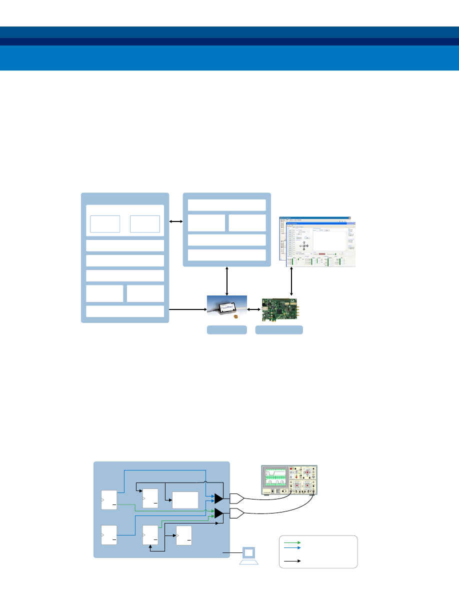
FPGA Design Flow
Design
Libero SoC
IP Catalog
Smart
Design
Simulation
Synthesis
Layout
Timing
Analysis
Power
Analysis
Hardware Debug
Embedded Design Flow
Complier
Debugger
Soft Console IDE
Firmware
Catalog
Sample
Projects
Programmer
Demo/Eval Board
Graphical Configurators
& Applications
Design Tools for Microsemi FPGAs and SoC FPGAs
SmartDebug
SmartDebug tool is a new approach to debug the Microsemi FPGAs and SERDES without using an integrated logic analyzer(ILA).
SmartDebug utilizes the dedicated and specialized probe points built into the FPGA fabric, which significantly accelerates and
simplifies the debug process. It also provides the ability to select different probe points without additional overhead and saves
significant recompile time. SmartDebug supports IGLOO2, SmartFusion2, and RTG4 FPGA families only. The enhanced debug
features implemented in these FPGAs give access to any logic element and enable designers to check the state of inputs and
outputs in real time, without any need to re-design.
• Uses minimal FPGA resources
for debug
• Active probes support static
and pseudo static signals
• Live probe supports dynamic
signals
• Requires no recompilation or
re-programming
• Has observability and
controllability features
• Allows on-the-fly changing
of probe points
Libero
®
SoC
Microsemi’s Libero SoC design suite offers high productivity with its comprehensive, easy-to-learn, easy-to-adopt development tools
that are used for designing with Microsemi’s power-efficient flash-based devices.
The Libero SoC design suite manages the entire design flow from design entry, synthesis, and simulation, through place-and-
route, timing, and power analysis, with enhanced integration of the embedded design flow. The suite integrates industry-standard
Synopsys Synplify Pro synthesis and Mentor Graphics ModelSim simulation with best-in-class constraints management, debug
capabilities, timing analysis, power analysis, secure production programming, and push button-design flow.
The Libero SoC design suite features an intuitive design flow with GUI wizards to guide the design process. Its easy-to-adopt,
single-click synthesis-to-programming flow integrates industry-standard third-party tools, and a rich IP library of DirectCores and
CompanionCores, and it supports complete reference designs and development kits.
19
Product Family
Device
Software
License Type
Libero
IDE
Libero
SoC
Libero
SoC
PolarFire
Eval
(Free)
Silver
(Free)
Gold
Platinum/
Standalone
PolarFire
MPF100T
×
×
×
×
×
MPF100, MPF200 (T & TS
devices), MPF300 packages on
eval boards only
×
×
×
×
All PolarFire devices
×
×
×
SmartFusion2, IGLOO2
M2S005, M2S010, M2S025
(T devices included) M2GL005,
M2GL010, M2GL025 (T devices
included)
×
×
×
×
×
All SmartFusion2 and IGLOO2
devices including S devices
×
×
×
×
SmartFusion, IGLOO,
ProASIC3, Fusion
All Devices
×
×
×
×
×
ProASIC and ProASIC
PLUS
All Devices
×
×
×
Axcelerator
AX125, AX250, AX500, AX1000
×
×
×
AX2000
×
×
SX-A, eX, MX
All Devices
×
×
×
Evaluation
Silver
Gold
Platinum
Standalone Archive
Standalone (1 yr)
Validity
30 days
1Yr
1Yr
1Yr
Permanent
(No Upgrades)
1Yr
DirectCores
Libero IP bundle
obfuscated and
selected RTL IPs
Libero IP bundle
obfuscated and
selected RTL IPs
Libero IP bundle
obfuscated and
selected RTL IPs
RTL for Libero IP
bundle cores
RTL for Libero IP
bundle cores
Libero IP bundle
obfuscated and
selected RTL IPs
Simulation
ModelSim ME
ProMixed lan-
guage simulation
ModelSim ME
Single language
simulation
ModelSim ME Pro
Mixed language
simulation
ModelSim ME Pro
Mixed language
simulation
Not applicable
Not applicable
Synthesis
Synplify Pro
Synplify Pro
Synplify Pro
Synplify Pro
Not applicable
Not applicable
Programming
Not Supported
Supported
Supported
Supported
Supported
Supported
Identify
Not Supported
Supported
Supported
Supported
Not Supported
Not Supported
Libero Device Support
License Types
Licensing Information
20
Part Number
Supported Device
Price
MPF300-EVAL-KIT-ES
MPF300TS-1FCG1152EES
$1495
Part Number
Supported Device
Price
MPF300-SPLASH-KIT-ES
MPF300TS-1FCG484EES
$699
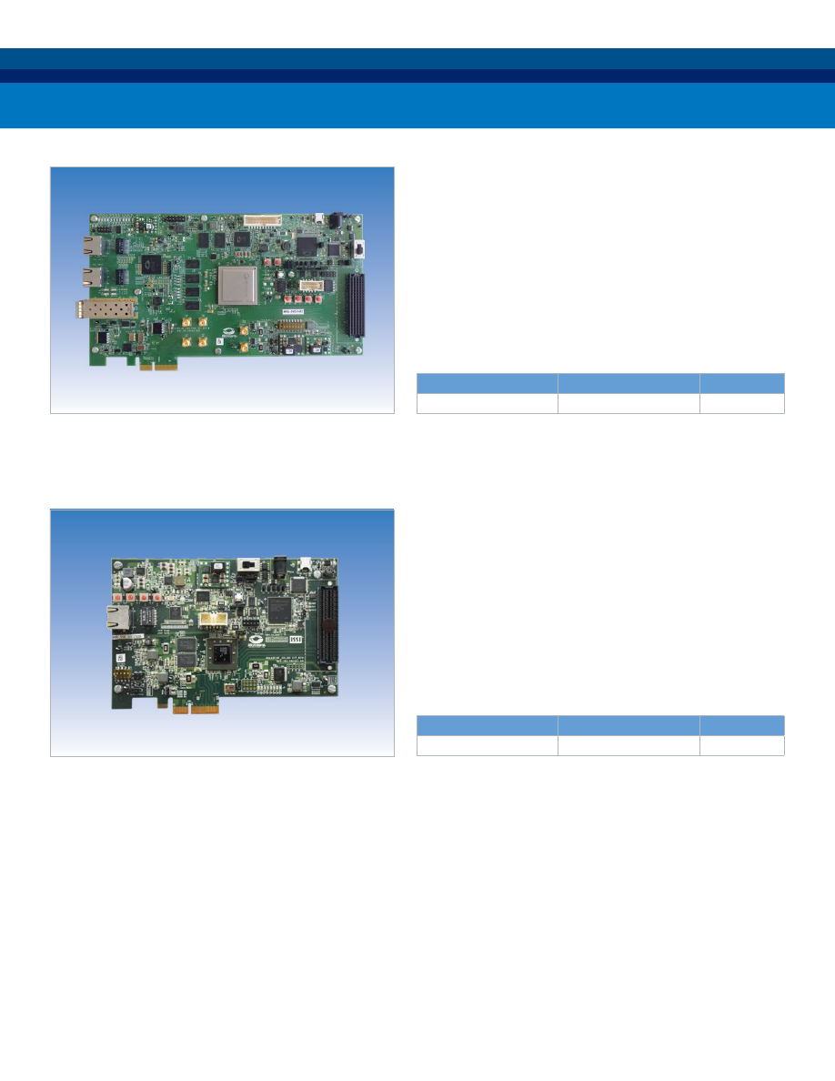
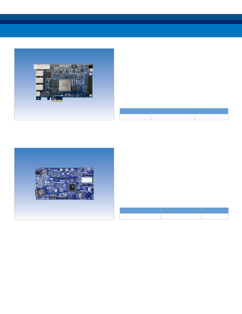
• RJ45 port with PHY for SGMII applications
• FMC connector (LPC)
• Prototype breadboard area
• PCI express (x4) edge connector
• On-board 50 MHz system clock
• 4GB 32-bit DDR4, 2GB 16-bit DDR3, and 1Gb SPI Flash Memory
• 2x RJ45 ports with PHY for Ethernet 1588 applications
• Support for SFP+ interface and IOG loopback
• High-speed SerDes interface
• 4x FMC connector (HPC)
• In-silicon temperature monitoring
• On-board 50 MHz system clock
PolarFire Evaluation Kit
PolarFire Splash Kit
Development Kits
21
Part Number
Supported Device
Price
AVMPF300TS-01
MPF300TS-FCG484EES
$179.95
Part Number
Supported Device
Price
AVMPF300TS-01
MPF300TS-1FCG1152EES
$499
Arrow PolarFire Everest Kit
• 1GbE interface with PHY (VSC8531)
• WiFi module
• Expansion connectors: Arduino Shield, MikroBus, PMOD
• DDR3 SDRAM (256Mx16)
• SFP cage
• 64 Mbit SPI Flash
• Other low-speed interfaces: UART and JTAG
• Triple 1GbE interface
• 1 × 10GbE SFP+ cage
• PCI express (x4) Gen2
• Dual DDR3L (x32 and x16)
• High-speed FMC (HPC) expansion
• HDMI output
• Expansion connectors: PMOD
• Other low-speed interfaces: UART, SPI, and I2C
Future PolarFire Avalanche Board
Development Kits
22
On/Off
Switch
50 Mhz
Oscillator
LPDDR
GPIO
Header
SW5
LEDs JTAG Programming
Header
Reset
Switch
ETM Trace
Debug
Header
RVI/IAR
Debug
Header
12 V Power
Supply Input
10/100/1000
Ethernet RJ45
Connector
USB-UART
Terminal
MicroUSB
OTG
SERDES
Reference
Clock
SW1
x1 PCle Edge
Connector
On Board
125 Mhz
SmartFusion2
SW4
SW2
SW3
SPI
Flash
Current Measurement
Current Measurement
TX/RX
SERDES
SMA
Pairs
I2C
Header
LP
Crystals
USB-UART
Terminal
10/100/1000
Ethernet RJ45
Connector Port0
10/100/1000
Ethernet RJ45
Connector Port1
USB Micro-AB
OTG Connector
Marvel
PHY
x4 PCIe
Edge Connector
DDR3
Memory
SmartFusion2 SPI
Flash
Debug
LEDS
Debug
Switch
RVI/IAR
Header
Power
Management
Reset
Switch
FT4232 Header
FMC Connecter
HPC
SERDES3
TX/RX
SMA Pairs
SERDES3
Reference
Clock
Bread
Board
Space
DIP
Switch
I2C
Header
On-Off
Switch
12V
Power Supply
Input
Debug
Switch
JTAG
Programming
Header
FMC
Connector
LPC
ETM Trace
Debug Header
User
Button
Reset
Button
64 MB
LPDDR
16 MB
SPI Flash
JTAG I/F
JP2
Ethernet
PHY
SmartFusion2
M2S SOM
(System-On-Module)
Breadboard
Area
Ethernet I/F
USBPower &
USB UART I/F
LEDs
JP3
JP1
HS USB
OTG
Interface
Part Number
Supported Device
Price
M2S090TS-EVAL-KIT
M2S090TS-FGG484
$399
Part Number
Supported Device
Price
SF2-STARTER-KIT
M2S050-FGG484
$299
SF2-484-STARTER-KIT
M2S010-FGG484
$299
SF2060-STARTER-KIT
M2S060-FGG484
$299
Part Number
Supported Device
Price
M2S150-ADV-DEV-KIT
M2S150TS-1FCG1152
$999
• Evaluate the data security features of
SmartFusion2 SoC FPGAs
• Develop and test PCI Express Gen2 x1
lane designs
• Test the signal quality of the FPGA
transceiver using full-duplex SERDES
SMA pairs
• Measure the low power consumption
of the SmartFusion2 SoC FPGA
• Quickly create a working PCIe link with
the included PCIe control plane demo
• Kit includes free 1-year Gold Libero
SoC license
• Board features
- 90 K LE SmartFusion2 device
- 64 Mbit SPI flash memory
- 512 MB LPDDR
- PCI Express Gen2 x1 interface
- Four SMA connector for testing of
full-duplex SERDES channel
- RJ45 interface for
10/100/1000 Ethernet
- JTAG/SPI programming interface
- Headers for I
2
C, SPI, GPIOs
- Push-button switches and LEDs
for demo purposes
- Current Measurement Test Points
• Full featured kit to develop
applications using SmartFusion2
SoC FPGAs
• Enables power measurement
• Two FMC connectors with HPC/LPC
pinout for expansion
• Various communication interfaces,
switches, and LEDs for prototyping
• Kit comes with free 1-year Gold Libero
SoC license
• Board features
- 150K LE SmartFusion2 device
- DDR3 SDRAM, SPI flash
- Current measurement test points
- A pair of SMA connectors, two FMC
connectors, PCIe x4 edge connector
- 2xRJ45 interface for 10/100/1000
Ethernet USB micro-AB connector
- FTDI programmer interface to
program the external SPI flash
- JTAG/SPI programming interface,
RVI header for application
programming, and debug
- Quad 2:1 MUX/DEMUX high-
bandwidth bus switch
- Dual in-line package (DIP) switches
for user application
- Push-button switches and LEDs
for demo purposes
• Cost-efficient development platform for
SmartFusion2 SoC FPGA
• Supports industry-standard interfaces,
including Ethernet, USB, SPI, I
2
C, and
UART
• Preloaded with uClinux image to
support Linux-based development
environments
• Comes with FlashPro4 programmer,
USB cables, and USB WiFi module
• Board features
- 50K LE or 10K LE
SmartFusion2 device
- JTAG interface for programming
and debug
- 10/100 Ethernet
- USB 2.0 On-The-Go
- 64 MB LPDDR, 16 MB SPI
flash memory
- Four LEDs and two push-button
switches
SmartFusion2 Starter Kit
SmartFusion2 Advanced Development Kit
SmartFusion2 Security Evaluation Kit
Development Kits
23
Current
Measurement
LP
Crystals
On Board
125 Mhz
12 V Power
Supply Input
On/Off
Switch
10/100/1000
Ethernet
RJ45
Connector
SERDES
Reference
Clock
MicroUSB
OTG
LPDDR
50 Mhz
Oscillator
GPIO
Header
LEDs
JTAG Programming
Header
Reset
Switch
SW3
SW4
SW2
SW5
IGLOO2
x1 PCIe Edge
Connector
SW1
RVI/IAR
Debug
Header
I2C
Header
ETM Trace
Debug
Header
SPI
Flash
USB-UART
Terminal
Tx/Rx
SERDES
SMA
Pairs
Part Number
Supported Device
Price
M2GL-EVAL-KIT
M2GL010T-1FGG484
$399
Part Number
Supported Device
Price
M2S010-MKR-KIT
M2S010-TQG144
$33.75
available from Digi-Key
Part Number
Supported Device
Price
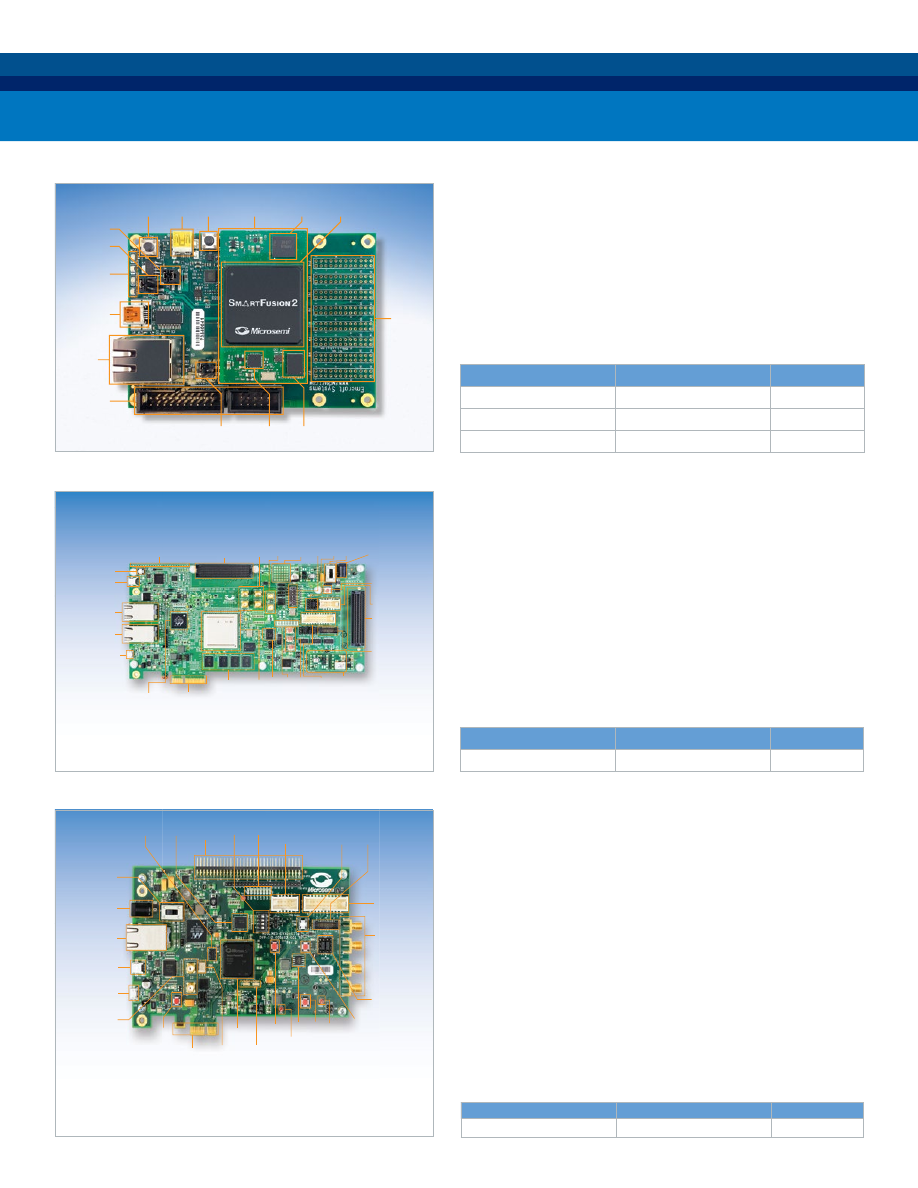
FUTUREM2GL-EVB
M2GL025
$99.95
(available from
Future Electronics)
www.microsemi.com/products/fpga-soc/design-resources/dev-kits-boards
Future’s IGLOO2 RISC-V Creative
Development Board includes
• Microsemi IGLOO2 FPGA
• Microsemi LX7167 DC/DC
• Alliance 32M × 16-bit DDR2
synchronous DRAM (SDRAM)
• Microchip 64 Mbit serial flash
• Microchip six synchronous sampling
16/24-bit resolution Delta-Sigma A/D
converters
• On-board FTDI USB-JTAG adaptor
• Arduino™-compatible expansion
headers
• MikroBUS™-compatible expansion
headers
• PMOD™-compatible expansion
connector
• User buttons and LED
• 25K (LE) FPGA, offering the lowest
cost-of-entry for both software and
hardware engineers who want to
evaluate and implement their own
unique designs
• Microsemi’s LX series power devices
Digikey SmartFusion2 Maker Board
• Gives designers access to IGLOO2
FPGAs that offer leadership in I/O
density, security, reliability, and low-
power for mainstream applications
• Supports industry-standard interfaces
including Gigabit Ethernet, USB 2.0
OTG, SPI, I
2
C, and UART
• Comes preloaded with a PCIe control
plane demo
• Can be powered by a 12 V power
supply or the PCIe connector, and
includes a FlashPro4 programmer
• Board features
- IGLOO2 FPGA in the FGG484
package (M2GL010T-1FGG484)
- JTAG/SPI programming interface
- Gigabit Ethernet PHY and
RJ45 connector
- USB 2.0 OTG interface connector
- 1 GB LPDDR, 64 MB SPI flash
- Headers for I
2
C, UART, SPI, GPIOs
- ×1 Gen2 PCIe edge connector
- Tx/Rx/Clk SMP pairs
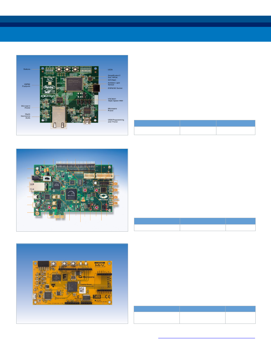
Devices: M2S010-MKR-KIT
• The SmartFusion2 M2S010 SoC FPGA
• USB Integrated FlashPro5
programming hardware
• The 10/100/1000BASE-T VSC8541
PHY
• Wurth Electronics RJ45 7499111221A
• Ambient Light Sensor
• 16Mbit SPI Flash
• USB port for UART communications
• 50 MHz clock source
IGLOO2 Evaluation Kit
Future IGLOO2 RISC-V Creative Development Board
Development Kits
24
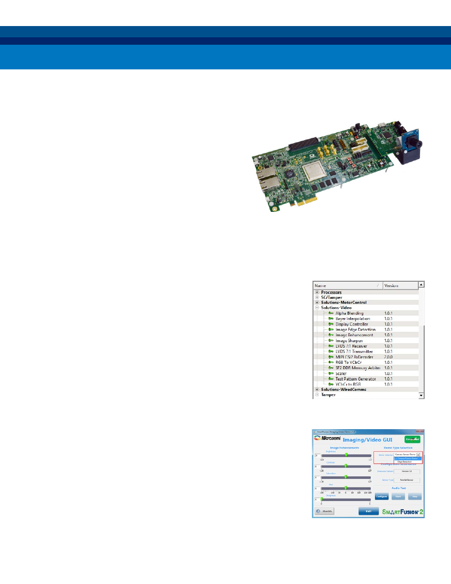
Microsemi provides a complete, easy-to-use development environment for designing low-power and secure video processing
applications. The solution includes an IP suite with modular IP, and FPGA mezzanine card (FMC) for the SmartFusion2 advanced
development kit, and a software GUI. The IP suite currently supports SmartFusion2 SoC FPGA and IGLOO2 FPGA product
families. Support for the PolarFire FPGA product family is currently in development.
Key Features
• Modular IP suite
• Support for MIPI CSI-2 or parallel sensor interfaces
• Display interface for 7:1 LVDS or HDMI
• The most secure FPGA to protect your design IP
• Easy-to-use software GUI for real-time audio and video configuration
Solution Overview
Hardware
• Imaging and video FMC daughter card with camera module options
• SmartFusion2 advanced development kit or PolarFire Evaluation Kit (Sold separately and includes a one-year Gold license of
Libero SoC software)
IP Suite
The following imaging and video processing IP cores are included in Libero® SoC,
a comprehensive software toolset for designing with Microsemi FPGAs and SoC FPGAs.
The IP suite supports SmartFusion2, IGLOO2 and RTG4 product families,
with PolarFire support currently in development
• Sensor interface—Parallel, MIPI CSI-2
• Bayer conversion
• Color-space conversion
• Image-edge detection
• Video scaler
• Alpha blending and overlay
• Image sharpening filter
• Image de-noising filter (under development)
• Display control (LVDS and parallel RGB-HDMI)
• Source code in Verilog (requires licensing fee)
Software GUI
Enables video and audio configurations
• GUI communicates with IP blocks through SmartFusion2 ARM
®
Cortex
®
-M3 processor
• Supports the following demos:
• Camera sensor to display
• Image edge detection
Software GUI for Imaging and Video Kit
Imaging and Video IP Cores in Libero SoC Catalog
MIPI CSI-2 or Parallel Sensor FMC daughter card options
(AR330 Image Sensor Board included)
Imaging and Video Solution
25
Field Oriented Control-System Diagram
Speed PI
Controller
Id-PI
Controller
Inverse Park
Transform
Inverse Clarko
Transform
SVPWM
Current
Measurement
Clarke
Transform
Park
Transform
Angle and
Speed
Estimation
Iq-PI
Controller
Speed
Ref
+
-
+
-
+
-
Speed
Actual
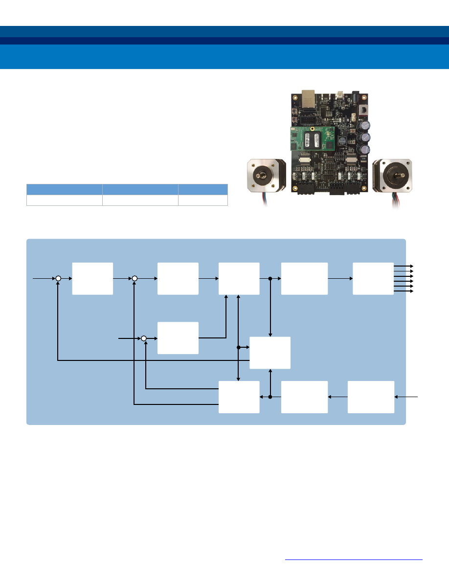
Id Actual
Id Actual
labc
l
αβ
θ
θ
Vd
Iq*
Iq*=0
Vq
V
αβ
Vabc
Ordering Code
Supported Device
Price
SF2-MC-STARTER-KIT
M2S010-FG484
$899
http://www.microsemi.com/applications/motor-control#overview
Reference Design Features
Build Safe and Reliable Deterministic Motor Control
Applications
Microsemi’s Deterministic Motor Control Solution is specially
designed to meet the challenging requirements of performance,
reliability, and safety in an easy-to-use environment. The solution is
compliant with industry coding standards for developing safe and
reliable software for embedded applications. Microsemi offers a
modular intellectual property (IP) portfolio, tools, reference designs,
kits, and software to control motors such as permanent-magnet
synchronous motor (PMSM)/brushless DC (BLDC), and stepper
motors.
• Dual-axis deterministic motor control on a single system-on-chip (SoC) field programmable gate array (FPGA)
• Efficient, reliable, and safe drive/motor control with product longevity
• Compact solution saves board space and reduces product size
• Motor performance is tested for speeds exceeding 100,000 RPM for sensorless field-oriented control (FOC)
• Low latency of 1 μs for FOC loop from ADC measurement to PWM enables switching frequencies up to 500 kHz
• Design flexibility with modular IP suite
• Advanced safety features, such as automatic motor restart and overcurrent protection
• SoC integration of system functions lowers total cost of ownership (TCO)
Motor Control Solution
26
Functionality
DirectCore Examples
Connectivity
UART,16550, 429, PCI, JESD204B
DSP
CIC, FFT, FIR, CORDIC, RS
Memory Controller
FIFO, DDR, QDR, SDR, MemCtrl, MMC
Processor
Cortex-M3, 8051, 8051s, ARM7TDMI
Ethernet
MII, RGMII, GMII, SGMII
Security
DES, 3DES, AES, SHA
Error Correction
EDAC, RC
Functionality
CompanionCore Examples
Connectivity
CAN, CANFD, PCIE, VME
DSP
FFT, JPEG, RS, DVBMOD
Memory Controller
SDRAMDDR, Flash, SD
Processor
80188, 80186, LEON3, 6809
Security
MD5, ARC4, RNG, ZUC, AES, SHA,
802.1ae (MACSec)
Error Correction
RS
Notes:
1. Additional cores and configurations can be found on the website and in core handbooks.
Product Name
Obfuscated RTL Available for Purchase
RTL Source Available for Purchase
CoreFFT
Not available
RTL source
Core1553BRM
Obfuscated RTL
RTL source
Core1553BRT, Core1553BRT_APB
Obfuscated RTL
RTL source
Core429, Core429_APB
Obfuscated RTL
RTL source
CorePCIF, CorePCIF_AHB
Obfuscated RTL
RTL source
CoreTSE, CoreTSE_AHB
Obfuscated RTL
RTL source
CoreCIC
Not available
RTL source
Microsemi enhances your design productivity by providing an extensive suite of proven and optimized IP Cores for use with
Microsemi FPGAs and SoC FPGA that covers key markets and applications. IPs are organized as either Microsemi-developed
DirectCores
TM
or third-party-developed CompanionCores.
TM
IP cores are searchable at:
http://soc.microsemi.com/products/ip/search/default.aspx
Microsemi DirectCore
Microsemi develops and supports DirectCore IP cores
for applications with the widest possible interest. Most
DirectCores are available for free within our Libero tool suite.
Common communications interfaces, peripherals, and
processing elements are all available as DirectCores. The
following table shows Microsemi’s DirectCore offerings.
Microsemi CompanionCore
Microsemi CompanionCore Partners use their detailed
system knowledge of common applications to craft
optimized solutions targeted for Microsemi FPGAs and SoC
FPGA. CompanionCores are available for purchase from
our partners and are easily integrated into your design using
our Libero tool suite. The following table shows examples of
CompanionCore Partners offerings.
Please contact your local Microsemi sales representative for information on price and licensing, as certain Microsemi IPs
may require a separate license. CompanionCores supported by Microsemi are available at:
http://www.microsemi.com/products/fpga-soc/design-resources/ip-cores#companioncores
Microsemi Intellectual Property
Microsemi IP Available for Use with Libero

27
PolarFire IP and Demo Designs
PolarFire IP (Available Now)
• AXI4Interconnect
• Core3DES
• CoreABC
• CoreAHBLite
• CoreAHBL2AHBL Bridge
• CoreAHBLTOAXI
• CoreAHBLSRAM
• CoreAHBtoAPB3
• CoreAPB3
• CoreAXI4DMA Controller
• CoreAXI4SRAM
• CoreAXItoAHBL
• CoreCORDIC
• CoreDDRMemCtrlr
• CoreDDS (NCO)
• CoreDES
• CoreFFT
• CoreFIFO
• CoreFIR
• CoreGPIO
• CoreI2C
• CoreJESD204BRX
• CoreJESD204BTX
• CoreMDIO_APB
• CorePCS
• CorePWM
• CoreRSDEC
• CoreRSENC
• CoreRISCV
• CoreRMII
• CoreSPI
• CoreSysServices_PF
• CoreUART
• CoreUART_APB
• CoreLSM
• CPRI (PHY only)
• CRYPTO
• DDR3
• DPSRAM
• DRI
• PCIe End Point
• TAMPER
• TPSRAM
• UPROM
• URAM
• 1GbE IO-CDR
• Core10GMAC 10GBASE-R
• Core429
• CoreSGMII
• CoreTSE, CoreTSE_AHB
• DDR4
• CoreRGMII
PolarFire IP (Soon to Be Released)
• CorePCIF/CorePCIF_AHB
• HD-SDI Tx/HD-SDI Rx (3G)
• CoreXAUI
• CoreRXAUI
• Core1553BRM
• Core1553BRT/Core1553BRT_APB
• PCIe Root Port
• CoreQDR
• 10GBASE-KR
• LPDDR3
• 10G NGPON
• CSI-2 Rx
• QSGMII
• 12G SDI
• CoreCIC
• CoreQSPI
• CSI-2 Tx
• CoreSquareRoot
• Fixed Point to Floating
Microsemi enhances your design productivity by providing an extensive suite of proven and optimized IP cores for use with
Microsemi FPGAs. Our extensive suite of IP cores covers all key markets and applications. Our cores are organized as either
Microsemi-developed DirectCores or third-party-developed CompanionCores. Most DirectCores are available for free within our
Libero tool suite and include common communications interfaces, peripherals, and processing elements.
PolarFire IP
MS2-004-15 55700049-06/1.18
©2018 Microsemi Corporation. All rights reserved.
Microsemi and the Microsemi logo are registered
trademarks of Microsemi Corporation. All other
trademarks and service marks are the property
of their respective owners.
Microsemi makes no warranty, representation, or guarantee regarding the information contained herein or the suitability of its products and services for any
particular purpose, nor does Microsemi assume any liability whatsoever arising out of the application or use of any product or circuit. The products sold
hereunder and any other products sold by Microsemi have been subject to limited testing and should not be used in conjunction with mission-critical equipment
or applications. Any performance specifications are believed to be reliable but are not verified, and Buyer must conduct and complete all performance and other
testing of the products, alone and together with, or installed in, any end-products. Buyer shall not rely on any data and performance specifications or parameters
provided by Microsemi. It is the Buyer’s responsibility to independently determine suitability of any products and to test and verify the same. The information
provided by Microsemi hereunder is provided “as is, where is” and with all faults, and the entire risk associated with such information is entirely with the Buyer.
Microsemi does not grant, explicitly or implicitly, to any party any patent rights, licenses, or any other IP rights, whether with regard to such information itself
or anything described by such information. Information provided in this document is proprietary to Microsemi, and Microsemi reserves the right to make any
changes to the information in this document or to any products and services at any time without notice.
Microsemi Corporation (Nasdaq: MSCC) offers a comprehensive portfolio of semiconductor and system solutions for aerospace
& defense, communications, data center and industrial markets. Products include high-performance and radiation-hardened
analog mixed-signal integrated circuits, FPGAs, SoCs and ASICs; power management products; timing and synchronization
devices and precise time solutions, setting the world’s standard for time; voice processing devices; RF solutions; discrete
components; enterprise storage and communication solutions, security technologies and scalable anti-tamper products;
Ethernet solutions; Power-over-Ethernet ICs and midspans; as well as custom design capabilities and services. Microsemi is
headquartered in Aliso Viejo, California and has approximately 4,800 employees globally. Learn more at www.microsemi.com.
Microsemi Corporate Headquarters
One Enterprise, Aliso Viejo, CA 92656 USA
Within the USA: +1 (800) 713-4113
Outside the USA: +1 (949) 380-6100
Fax: +1 (949) 215-4996
Email: sales.support@microsemi.com
www.microsemi.com
Microsemi is continually adding new products to its
industry-leading portfolio.
For the most recent updates to our product line and for detailed
information and specifications, please call, email, or visit our website.
Toll-free: 800-713-4113
sales.support@microsemi.com
www.microsemi.com