ETALDOC 339/8
Page 1 of 7
January 2001
PRODUCT DATA SHEET
ISDN S
o
INTERFACE TRANSFORMER
P2880
Features
Applications
∗
Ultra-low profile, 7mm
∗
Basic Rate ISDN
∗
Excellent pulse shape
∗
IEC 950, EN 60950 and EN 41003 certified
∗
CSA NRTL/C Certificate of Compliance
∗
BABT Certificate of Recognition
∗
Vacuum encapsulated
DESCRIPTION
P2880 is a microprofile transformer for ISDN S
o
applications requiring safety-critical isolation to
international standards.
P2880 is designed specifically for S
o
ISDN
interfaces complying with CCITT (ITU-T) I.430
Basic Rate requirements (2B + D at 192kbits/s).
P2880 is certified to safety standards IEC 950,
EN 60950 and EN 41003 for supplementary
insulation, 250V working voltage. P2880 is
supported by an IEC CB Test Certificate, CSA
Certificate of Compliance and BABT Certificate.
The requirements of I.430 are easily achieved
due to propriety construction which yields low
leakage inductance and coupling capacitance
whilst being fully compliant with international
safety requirements.
to Electronic Techniques
(Anglia) Limited
p2880-html.html
P2880
ETALDOC 339/8
Page 2 of 7
January 2001
SPECIFICATION
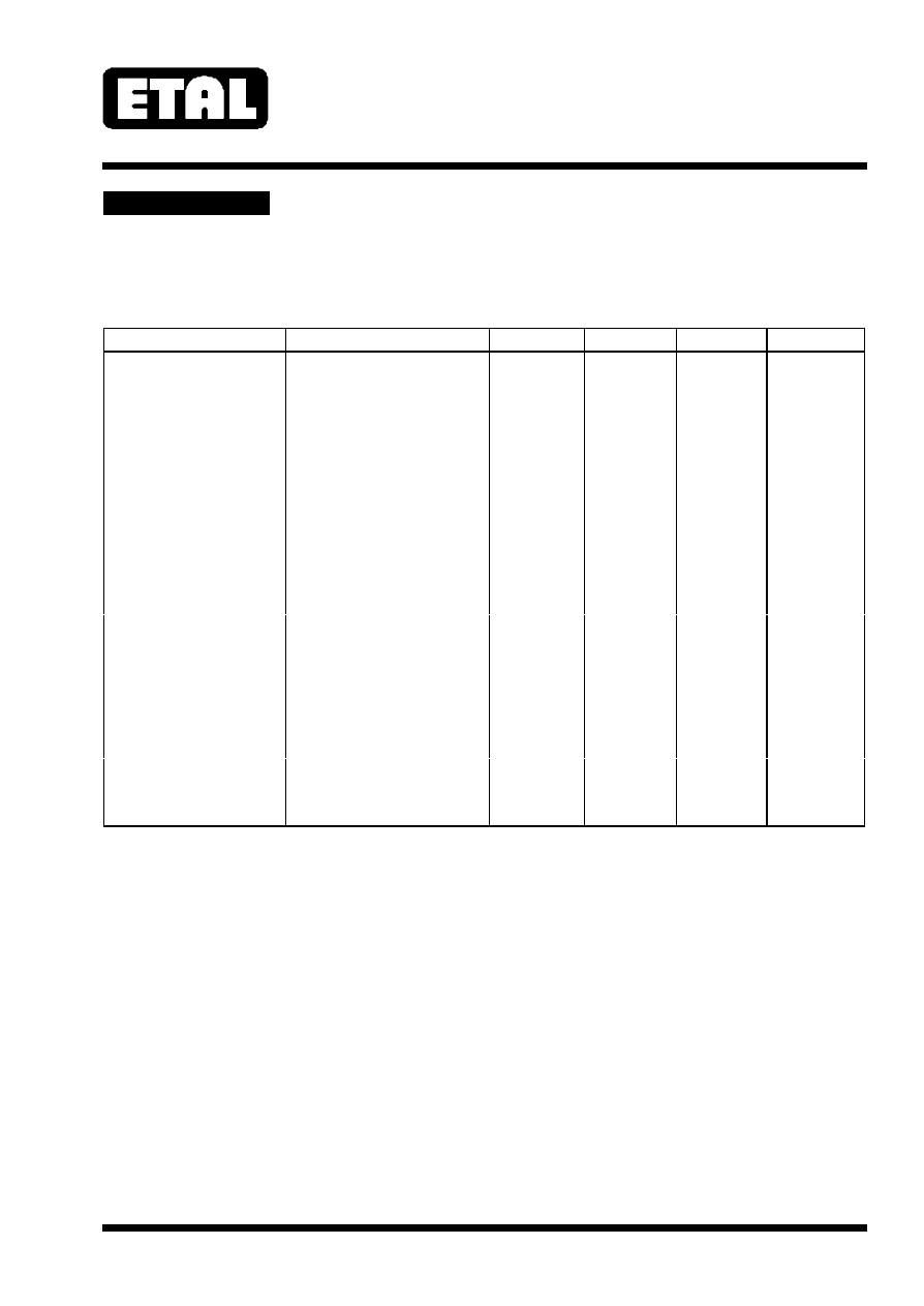
Electrical
At T = 25ºC and with pins 4 & 5 joined unless otherwise stated. The convention used in this datasheet is that
'primary' windings are on the line side and 'secondary' windings are on the IC side.
Parameter
Conditions
Min
Typ
Max
Units
Turns ratio
(1-2) : (3-5)+(4-6):
1.97
2.00
2.03
Primary inductance
3-6
2kHz, 100mV
10kHz, 100mV
20kHz, 100mV
23
23
22
36
32
32
-
-
-
mH
mH
mH
Leakage inductance
3-6 (1 and 2 linked) 10kHz
-
4
10
µH
Shunt loss
3-6
2kHz 100mV
10kHz 100mV
-
20
8
-
-
-
k
Ω
k
Ω
Winding DC resistance
3-6
1-2
-
-
3.6
4.0
-
-
Ω
Ω
Parallel capacitance
3-6
1-2
-
-
90
20
-
-
pF
pF
Interwinding
capacitance
1 & 2 linked to 3, 4, 5, 6
linked
-
30
-
pF
Voltage isolation
50Hz
DC
2.12
3.0
-
-
-
-
kVrms
kV
Operating range:
Functional
Storage
0
-40
-
-
+70
+125
ºC
ºC
p2880-html.html
P2880
ETALDOC 339/8
Page 3 of 7
January 2001
SPECIFICATION
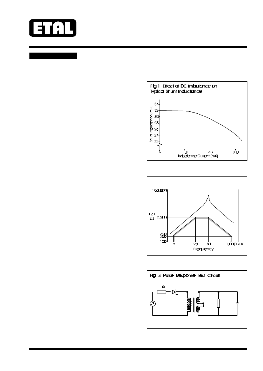
DC Imbalance
If required, P2880 will support a small degree of
DC current imbalance between its primary
windings, e.g. during phantom powering. DC
current imbalance, however, should be limited to
1mA if P2880 is fully to comply with its
specification. Fig 1 shows the effect of current
imbalance on typical primary inductance.
Input/Output impedance
In the inactive, powered down or binary ONE
transmission states the interface point must
present a high impedance in accordance with the
templates given in I.430 sections 8.5 and 8.6.
Fig 2 shows the typical primary impedance
characteristic of P2880 stimulated with 100mVrms
sinusoidal from 2kHz to 1MHz across pins 3 and 6
(4 & 5 linked) against the I.430 TE impedance
template.
Pulse response
Fig 3 shows the pulse response test circuit.
The schottky diode ensures that the source
presents a low impedance for a positive binary
ZERO and a high impedance for a binary ONE.
The 62Ù resistor and the winding resistances are
transformed into the primary circuit as 62/4 +4/4 +
3.6 = 20.1Ù, thus satisfying the I.430 requirement
for
≥
20Ù transmitter output impedance (para
8.5.1.1.(b)).
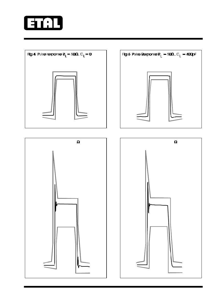
Pulse characteristics against I.430 pulse masks are
given for 50Ù and 400Ù terminations and for
50Ù//400pF and 400Ù//400pF loads, figs 4-7.
400pF represents a typical EMC capacitance fitted
across the primary in conjunction with a 10 metre
(maximum length) connecting cord with maximum
permissible capacitance of 350pF (I.430, 8.9(b)).
On the 400Ù//400pF combination, the pulse trailing
edge decay profile is almost completely determined
by the R
L
C
L
time constant (160ns).
Fig 2 Impedance Characteristic
C
L
R
L
2
3
4
5
6
BAT85
2:1
1
62
P2880
p2880-html.html
P2880
ETALDOC 339/8
Page 4 of 7
January 2001
Fig 7 Pulse Response R = 400 , C = 400pF
L
L
Fig 5 Pulse response R =400 , C =0
L
L
p2880-html.html
P2880
ETALDOC 339/8
Page 5 of 7
January 2001
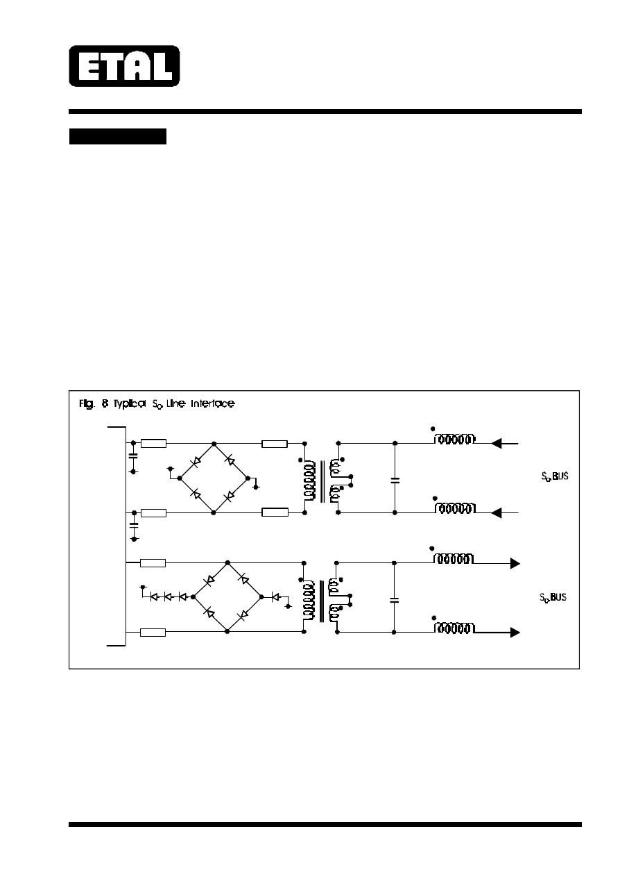
APPLICATION
Applications vary depending on chipset choice and
circuit requirements. A typical line interface will
address the following:
1.
Input/output high impedance masks which
must be satisfied even in the inactive and
powered-down mode.
2.
Output impedance in binary ZERO state
(
≥
20Ù).
3.
Pulse performance
4.
Longitudinal conversion loss (LCL) and
output signal balance (OSB).
5.
EMC.
6.
Overvoltage protection.
A starting point for a line-interface implementation
shown in figure 8.
The current-compensated quad choke is used to
achieve satisfactory LCL and OSB performance.
The diodes, which must be low capacitance type,
provide overvoltage protection. Each path to
supply rails is through at least 2 diodes to satisfy
the high impedance requirement in the presence
of signals.
At the chip RX inputs, 47pF capacitors in
conjunction with 10kÙ (max) series resistance
provide attenuation of high frequency noise.
The 33Ù resistors at the chip TX output set the
pulse amplitude in the bus to the correct level and
ensure an output impedance at the line of >20Ù.
1.8k
Ω
1.8k
Ω
8.2k
Ω
8.2k
Ω
56nF
47pF
47pF
RX1
RX2
RX2
TX2
TX1
RX1
2
3
1
7
8
2
5
6
1
0V
0V
P2880
Vcc
0V
33Ω
33Ω
56nF
4 X 4mH
ETAL P2910
TX+
TX-
2
3
4
3
5
6
4
5
6
1
0V
Vcc
P2880
p2880-html.html
P2880
ETALDOC 339/8
Page 6 of 7
January 2001
CHIPSET COMPATIBILITY
The 2:½+½ transformer ratio is suitable for a
number of chipsets including:
Siemens PEB 2080
Siemens PEB 2081
Siemens PEB 2085
Siemens PEB 2086
National TP 3420
Mitel MT 8930
AMD AM 79C30A
For chipsets requiring 1:½+½ transformer ratio
(e.g. Motorola MC145474), ETAL® P2881 is
available.
For volume applications, variants can be supplied
to satisfy the requirements of any other chipset.
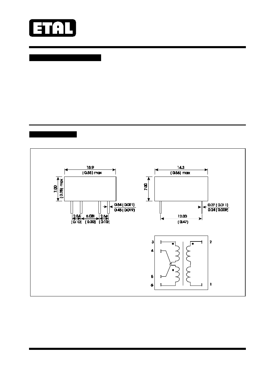
CONSTRUCTION
Dimensions shown are in millimetres (inches).
Geometric centres of outline and pin grid coincide within a tolerance circle of Ø0.6mm.
Recommended PCB hole size Ø0.8mm.
Terminal pins electroplated Sn Pb 60/40 µm min.
Fig 9 Mechanical Specification
p2880-html.html
P2880
ETALDOC 339/8
Page 7 of 7
January 2001
SAFETY
ABSOLUTE MAXIMUM RATINGS
(Ratings of components independent of circuit).
Short term isolation voltage (1s)
2.12kVrms
3.0kVDC
Storage temperature
-40ºC to
+125ºC
Constructed in accordance with IEC 950:1991,
EN 60950:1992 (BS 7002:1992), supplementary
insulation and BS EN 41003:1997, 250Vrms
working.
Lead temperature, 10s
260ºC
CERTIFICATION
COPYRIGHT
Certified by BSI to IEC 950:1991/A4:1996 (IEC CB
Test Certificate No. GB541W) sub-clauses 2.2.2,
2.9.2, 2.9.3, 2.9.4, 2.9.6, 2.9.7, 4.4, 4.4.3.2 (class
V-0) and 5.3 for a maximum working voltage of
250Vrms, nominal mains supply voltage not
exceeding 300Vrms and a maximum operating
temperature of +70ºC in Pollution Degree 3
environment, supplementary insulation.
CAN/CSA C22.2 No. 950-95/UL1950, certified by
CSA, Third Edition, including revisions through to
revision date March 1, 1998, based on Fourth
Amendment of IEC 950, Second Edition, maximum
working voltage 250Vrms, Pollution Degree 2,
supplementary insulation.
CSA Certificate of Compliance 1107696 (Master
Contract 1188107).
Certified by BABT to EN 60950.
BABT Certificate CR/0160.
Additionally, Profec Technologies certifies all
transformers as providing voltage isolation of
2.12kVrms, 3kV DC minimum. All shipments are
supported by a Certificate of Conformity to current
applicable safety standards.
ETAL and P2880 are Trade Marks of Profec
Technologies Ltd.
The Trade Mark and Service Mark ETAL are
registered at the UK Trade Marks Registry.
Profec Technologies Ltd. is the owner of the
design right under the Copyright Designs and
Patents Act 1988 and no rights or licences are
hereby granted or implied to any third party.
© 1995, 2000 Profec Technologies Ltd.
Reproduction prohibited.
T R A N S F O R M I N G T H E F U T U R E
Profec Technologies Ltd, 10 Betts Avenue, Martlesham Heath, Ipswich, IP5 3RH, England
Telephone: +44 (0) 1473 611422
Fax: +44 (0) 1473 611919
Websites: www.etal.ltd.uk
www.profec.com
Email:
info@etal.ltd.uk
sales@profec.com
ISO 9001
FM 25326