ETALDOC 591/8
Page 1 of 5
January 2001
PRODUCT DATA SHEET
LOW COST, LOW DISTORTION
P3356
LINE MATCHING TRANSFORMER
Features
Applications
∗
Low Cost
∗
V.90 and V.92 Modems
∗
Low Distortion
∗
V.34 Modems
∗
12.6mm (0.5”) Seated Height
∗
Fax Machines
∗
Industry Standard Pinout
∗
Instrumentation
∗
IEC 950, UL 1950 and EN 60950 Certified
∗
UL Recognized Component
∗
BABT Certificate of Recognition
∗
Extended Frequency Response
∗
Flat TX and RX Responses
∗
Simple Matching
∗
Low Insertion Loss
∗
High Thermal Stability
DESCRIPTION
P3356 is intended for V.90 and V.92 (56kbps)
modems and other high-speed applications where
ultra-low distortion at moderate power levels and
very low voiceband frequencies is required at a
most competitive price.
P3356 uses patented design and construction
methods to achieve excellent signal performance
and safety isolation to international standards at
truly low cost, making it the component of choice
for high-speed data applications throughout the
world. P3356 is certified to IEC 950,
EN 60950, EN 41003, and CAN/CSA C22.2
No. 950-95/UL1950. P3356 is a UL Recognized
Component, and is supported by a BABT
Certificate of Recognition and an IEC CB Test
Certificate.
P3356 has exceptionally flat frequency response
from 30Hz to 10kHz, a 3dB bandwidth of over
50kHz and requires only the very simplest of
matching to achieve good return loss and
transhybrid loss across the voiceband, with very
low levels of signal distortion at signal
frequencies as low as 150Hz.
P3356 also exhibits stable characteristics over its
full operating temperature range to maximize
data throughput under varying environmental
conditions without the need for modem
retraining.
Patented
E203175
to Electronic Techniques
(Anglia) Limited
p3356-html.html
P3356
ETALDOC 591/8
Page 2 of 5
January 2001
SPECIFICATIONS
Electrical
At T = 25ºC and as circuit Fig. 2 unless otherwise stated.
Parameter
Conditions
Min
Typ
Max
Units
Insertion Loss
f = 2kHz, R
L
= 600
Ω
-
1.5
-
dB
Frequency Response
LF -3dB cutoff
HF -3dB cutoff
100Hz – 4kHz
-
-
-
10
55
-
-
-
±
0.1
Hz
kHz
dB
Return Loss
(5)
200Hz – 4kHz
16
-
-
dB
Transhybrid Loss
(5)
200Hz – 4kHz
20
-
-
dB
Third Harmonic
Distortion
(1)
150Hz -3dBm in line
200Hz -10dBm in line
-
-
-70
-89
-
-
dBm
dBm
Voltage Isolation
(2)
50Hz
DC
2.12
3.0
-
-
-
-
kVrms
kV
Operating Range:
Functional
Storage
0
-40
-
-
+70
+85
ºC
ºC
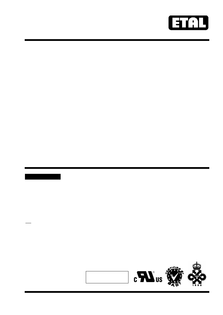
Lumped equivalent circuit parameters as Fig. 1
DC resistance
(3)
Primary resistance R
DCp
Secondary resistance R
DCs
70
95
-
-
87
120
Ω
Ω
Leakage inductance,
∆
L
3
3.9
5
mH
Shunt inductance, Lp
(4)
200Hz -43dBm
6
9
-
H
Shunt loss, Rp
200Hz -43dBm
12
15
-
k
Ω
Notes:
1. Third harmonic typically exceeds other
harmonics by 10dB.
2. Components are 100% tested at 3.25kVDC.
3. Caution: do not pass DC through windings.
Telephone line current must be diverted using
semiconductor line hold circuit or choke.
4. At signal levels greater than –20dBm, Lp will
increase and Rp will decrease slightly but the
effect is usually favourable to the return loss
characteristic.
5. Return loss and transhybrid loss can be
improved to 30dB in improved matching circuit.
The values shown relate to the simplest
configuration, Fig. 2.
Equivalent Circuit
Fig. 1
IDEAL
1:1
½ L
½ L
p3356-html.html
P3356
ETALDOC 591/8
Page 3 of 5
January 2001
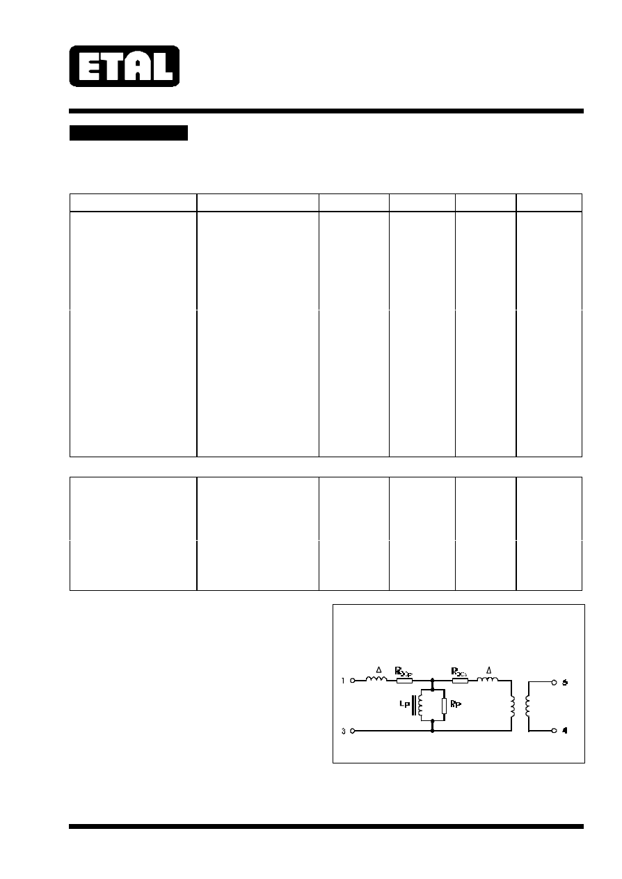
MATCHING RECOMMENDATIONS
The following recommendations start with the simplest implementations and progress to enhanced
performance utilizing additional components. Good performance is achieved even with the simplest
configurations. The implementations assume a low impedance balanced TX drive and a relatively high
impedance RX input, as is commonly available, though use with other TX/RX arrangements is
straightforward. Note that there are no changes to components on the line side, or in the hybrid, whether
600
Ω
or complex reference impedance selected, thus assisting country configuration. For complex
impedance, the matching circuits derived are suitable for reference impedances of the type 270 + 750//150nF
e.g. European CTR21 and 220 + 820//120nF (or 115nF) e.g. Australia, South Africa, etc., and yield similar
performance characteristics. For other impedances, please contact Profec Technologies.
Minimum Cost Implementations
Insertion Loss: 1.8dB @ 2kHz
Frequency Response : ±0.2dB 30Hz – 10kHz
Return Loss: 16dB 200Hz – 4kHz
Transhybrid Loss: 22dB 200Hz – 4kHz
Insertion Loss: 1.0dB @ 2kHz
Frequency Response : ±0.5dB 50Hz – 4kHz
Return Loss: 18dB 200Hz – 4kHz
Transhybrid Loss: 14dB 200Hz – 4kHz
Improved matching
Insertion Loss: 1.8dB @ 2kHz
Frequency Response : ±0.2dB 30Hz – 10kHz
Return Loss: 18dB 200Hz – 4kHz
Transhybrid Loss: 22dB 50Hz – 10kHz
Insertion Loss: 1.0dB @ 2kHz
Frequency Response : ±0.5dB 50Hz – 4kHz
Return Loss: 20dB 200Hz – 4kHz
Transhybrid Loss: 16dB 50Hz – 4kHz
600
Ω
Fig. 4
LINE
600
10nF
560
RXA
TXA2
TXA1
µ
2 2 F
600
Ω
Fig. 2
LINE
600
560
RXA
TXA2
TXA1
µ
2 2 F
10nF
LINE
270
(220)
750
(820)
µ
2 2 F
150nF
(120nF)
750
100nF*
*Note: 100nF capacitor should have a temperature stable dielectric
120
European CTR21/(Australia, etc.)
Fig. 5
RXA
TXA2
TXA1
LINE
270
(220)
750
(820)
150nF
(120nF)
820
100nF*
*Note: 100nF capacitor should have a temperature stable dielectric
100
European CTR21/(Australia, etc.)
Fig. 3
RXA
TXA2
TXA1
µ
2 2 F
Patented
p3356-html.html
P3356
ETALDOC 591/8
Page 4 of 5
January 2001
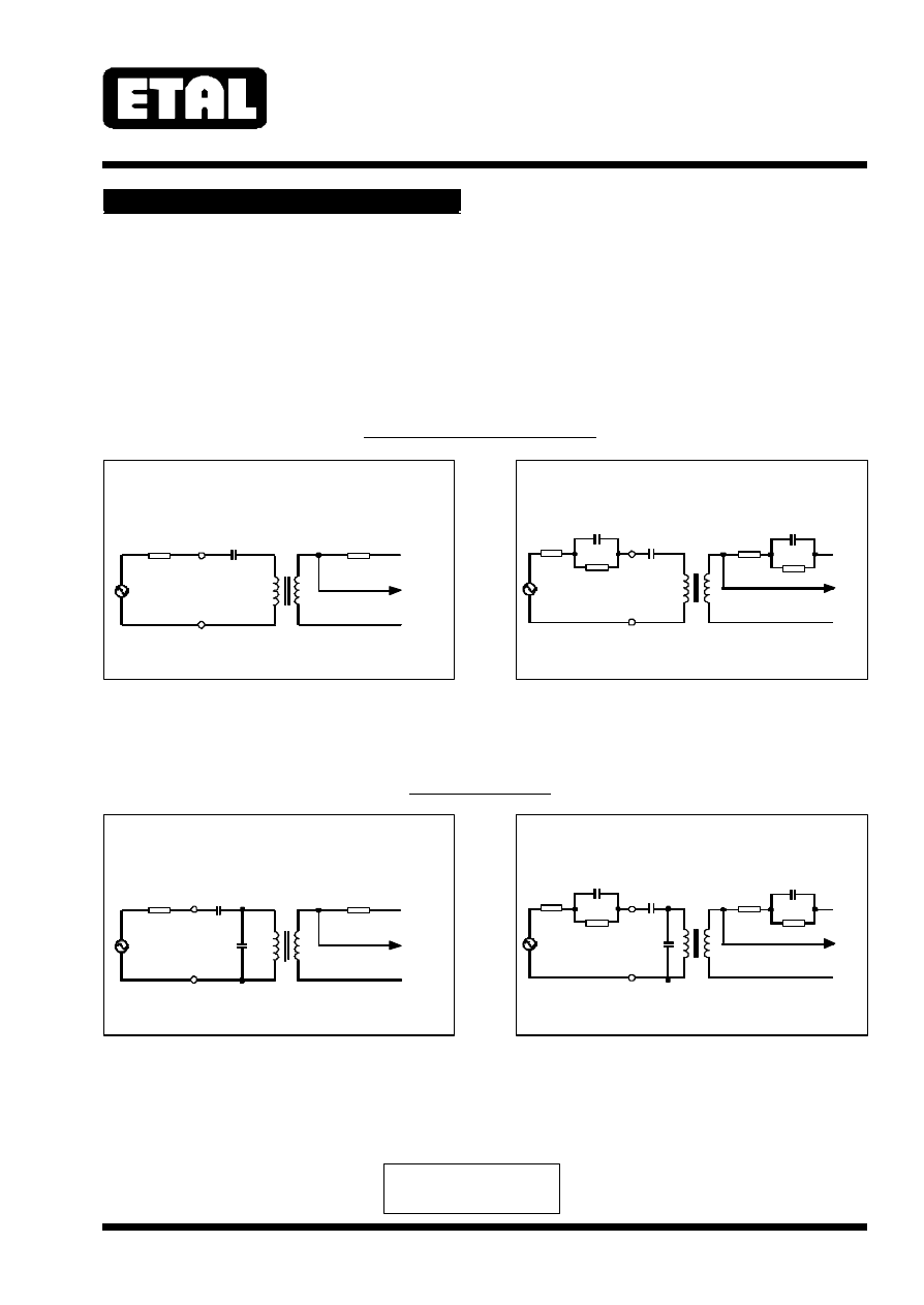
Improved matching and hybrid
Insertion Loss (Line to RXA): 2.8dB @ 2kHz
Frequency Response : ±0.2dB 30Hz – 10kHz
Return Loss: 20dB 200Hz – 4kHz
Transhybrid Loss: 30dB 50Hz – 10kHz
Insertion Loss (Line to RXA): 2.2dB @ 2kHz
Frequency Response : ±0.5dB 50Hz – 4kHz
Return Loss: 20dB 200Hz – 4kHz
Transhybrid Loss: 18dB 200Hz – 4kHz
600
Ω
Ω
Instrumentation
CERTIFICATION
Insertion Loss: 1.5dB @ 2kHz
Frequency Response : ±0.2dB 20Hz – 20kHz
Return Loss: 16dB 20Hz – 20kHz
SAFETY
Constructed in accordance with IEC 950:1991,
EN 60950:1992 (BS7002:1992) to amendment 5,
and UL1950 3rd Edition, supplementary insulation,
250Vrms maximum working voltage, flammability
class V-0.
There are no special installation requirements
(beyond attending to usual PCB track separations)
since the integral cover provides supplementary
insulation from its external faces to internal core
and windings.
Certified under the IEC CB scheme (Certificate
GB445W) to IEC 950:1991, up to amendment 4,
sub-clauses 1.5, 1.5.1, 1.5.3, 2.2, 2.2.3, 2.2.4, 2.9.2,
2.9.3, 2.9.4, 4.4, 4.4.3.2 (class V-0) and 5.3 for a
maximum working voltage of 250Vrms, nominal
mains supply voltage not exceeding 300Vrms
and a maximum operating temperature of 70ºC
in Pollution Degree 2 environments.
Recognized under the Component Recognition
Program of Underwriters Laboratories Inc. to US and
Canadian requirements CAN/CSA C22.2
No. 950-95/UL1950, Third Edition, including
revisions through to revision date March 1, 1998,
based on Fourth Amendment of IEC 950, Second
Edition, maximum working voltage 180Vrms
(creepage), 420V peak (clearance), Pollution
Degree 2, supplementary insulation.
UL File number E203175.
Approved and certified by BABT to EN 60950
and EN 41003.
BABT Certificate of Recognition 608755
Additionally, Profec Technologies certifies all
transformers as providing voltage isolation of
2.12kVrms, 3kV DC minimum. All shipments are
supported by a certificate of conformity to current
applicable safety standards.
600
Ω
Fig. 6
LINE
600
10nF
560
1k
1nF
10k
RXA
TXA2
TXA1
µ
2 2 F
10nF
1nF
LINE
270
(220)
750
(820)
µ
2 2 F
150nF
(120nF)
750
100nF*
*Note: 100nF capacitor should have a temperature stable dielectric
120
European CTR21/(Australia, etc.)
Fig. 7
RXA
TXA2
TXA1
1k
10k
µ
µ
47 F*
µ
47 F*
600
Ω
Fig. 8
600
Ω
600
Ω
6.8nF
6.8nF
* If no DC block required, one of these capacitors can be removed and
the other set to 22 F, or, if preferred, both capacitors can be eliminated.
Patented
p3356-html.html
P3356
ETALDOC 591/8
Page 5 of 5
January 2001
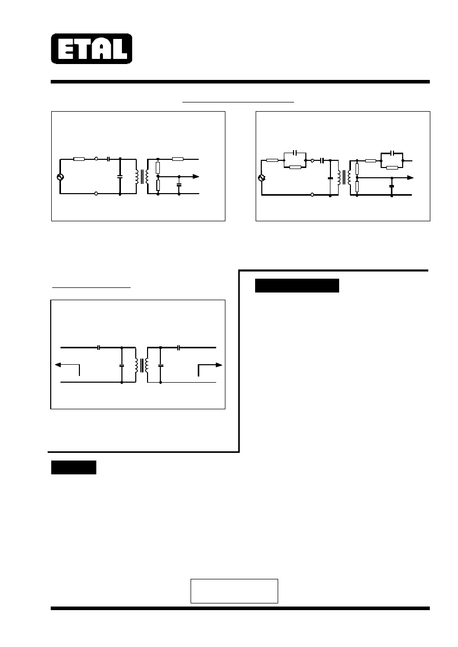
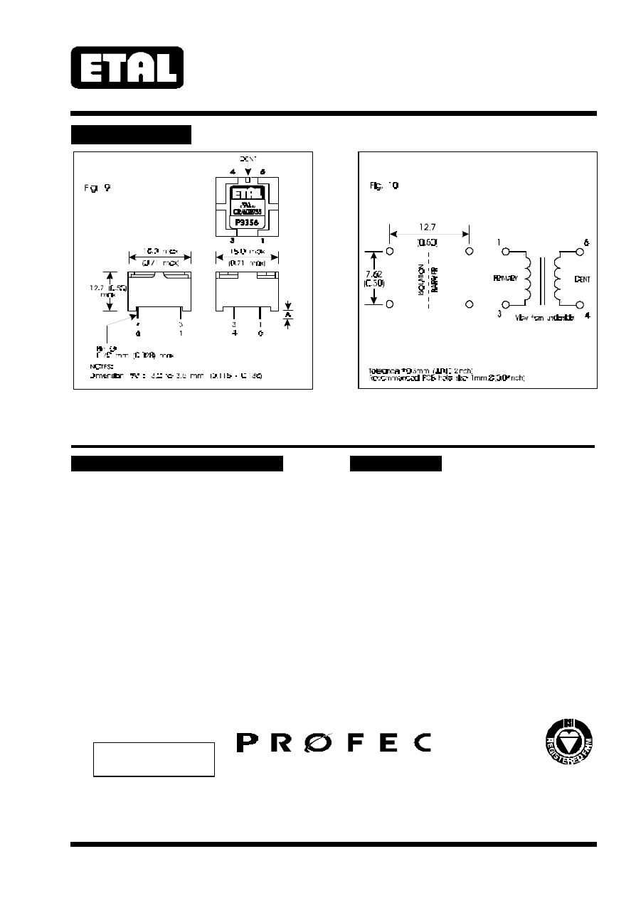
CONSTRUCTION
Dimensions shown are in millimetres (inches).
Geometric centres of outline and pin grid coincide within a tolerance circle of 0.6mmØ.
Windings may be used interchangeably as primary or secondary.
Total weight typically 6.3g.
ABSOLUTE MAXIMUM RATINGS
COPYRIGHT
(Ratings of components independent of circuit).
Short term isolation voltage (1s)
DC current
Storage temperature
Lead temperature, 10s
2.12kVrms,
3.0 kVDC
100
µ
A
-40ºC to
+85ºC
260ºC
ETAL and P3356 are Trade Marks of Profec
Technologies Ltd.
The Trade Mark ETAL is registered at the UK
Trade Marks Registry.
Profec Technologies Ltd. is the owner of the
design right under the Copyright Designs and
Patents Act 1988 and no rights or licences are
hereby granted or implied to any third party.
P3356 design and construction are protected by
patents and registered design.
British Patent No. 2333646.
British Patent No. 2340667.
UK Registered Design No. 2077360.
French Registered Design No. 991512.
Germany Registered Design 49902311.0.
United States Registered Design 426, 815.
Other patents and registered designs pending.
© 1998 - 2000 Profec Technologies Ltd.
Reproduction prohibited.
T R A N S F O R M I N G T H E F U T U R E
Profec Technologies Ltd., 10 Betts Avenue, Martlesham Heath, Ipswich, IP5 3RH, England
Telephone: +44 (0) 1473 611422
Fax: +44 (0) 1473 611919
Websites: www.etal.ltd.uk
www.profec.com
Email:
info@etal.ltd.uk
sales@profec.com
Patented
Connections
ISO 9001
FM 25326
Dimensions