MAXIMUM RATINGS AND ELECTRICAL CHARACTERISTICS
Ratings at 25
o
C ambient temperature unless otherwise specified.
Single phase, half wave, 60 Hz, resistive or inductive load.
For capacitive load, derate current by 20%.
SE6
THRU
SE1
SOD-123F
MAXIMUM RATINGS
(@ T
A
=25
O
C unless otherwise noted)
ELECTRICAL CHARACTERISTICS
(@T
A
=25
O
C unless otherwise noted)
Dimensions in inches and (millimeters)
RATINGS
Maximum Recurrent Peak Reverse Voltage
Maximum RMS Voltage
Maximum DC Blocking Voltage
Maximum Average Forward Rectified Current
at T
A
= 55
O
C
Peak Forward Surge Current 8.3 ms single half sine-wave
superimposed on rated load (JEDEC method)
Typical Thermal Resistance (Note 1)
Typical Junction Capacitance (Note 2)
SYMBOL
V
RRM
V
DC
I
FSM
C
J
T
STG
V
RMS
UNITS
Volts
Volts
Volts
Amps
1.0
15
130
15
10
Amps
0
C/W
0
C/W
0
C
Storage Temperature Range
R
q
J A
Typical Thermal Resistance (Note 1)
30
R
q
J L
I
O
pF
Operating Temperature Range
T
J
SE1
50
150
-55 to + 150
0
C
SE3
SE4
150
200
35
105
140
50
SE2
100
70
100
150
200
SE5
300
210
300
SE6
SE1
SE3
SE4
SE2
SE5
SE6
400
400
280
2006-12
CHARACTERISTICS
Maximum Average Reverse Current
at Rated DC Blocking Voltage
V
F
SYMBOL
I
R
m
A
Maximum Instantaneous Forward Voltage at 1.0A DC
Volts
5
350
@T
A
= 25
o
C
@T
A
= 100
o
C
m
A
UNITS
0.95
1.25
trr
Maximum Reverse Recovery Time (Note 4)
nSec
35
NOTES : 1. Thermal Resistance :Mounted on PCB.
2. Measured at 1 MHz and applied reverse voltage of 4.0 volts.
3. "Fully ROHS compliant","100% Sn plating (Pb-free)".
4. Test Conditions: I
F
= 0.5A, I
R
= -1.0A, I
RR
= -0.25A.
SURFACE MOUNT SUPER FAST RECTIFIER
VOLTAGE RANGE 50 to 400 Volts CURRENT 1.0 Ampere
FEATURES
* High reliability
* Low leakage
* Low forward voltage
* High current capability
* Super fast switching speed
* High surge capability
* Good for switching mode circuit
MECHANICAL DATA
* Case: Molded plastic
* Epoxy: Device has UL flammability classification 94V-O
* Lead: MIL-STD-202E method 208C guaranteed
* Mounting position: Any
* Weight: 0.016 gram
.150 (3.8)
.142 (3.6)
.035 (0.90)
.028 (0.70)
.053 (1.35)
.047 (1.20)
.077 (1.95)
.069 (1.75)
.030 (0.75)
.022 (0.55)
.008 (0.20)
.114 (2.9)
.106 (2.7)
AMBIENT TEMPERATURE, (
O
C)
IN
ST
AN
TA
NE
O
US
R
EV
ER
SE
C
UR
RE
NT
, (
uA
)
25
1.0
0
0
0.8
0.6
0.4
0.2
75
50
175
100
125
150
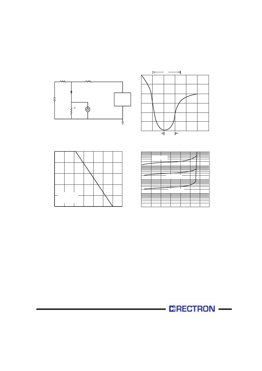
RATING AND CHARACTERISTICS CURVES ( SE1 THRU SE6 )
FIG.2 TYPICAL FORWARD CURRENT
DERATING CURVE
FIG.1 TEST CIRCUIT DIAGRAM AND REVERSE RECOVERY TIME CHARACTERISTIC
PERCENT OF RATED PEAK REVERSE VOLTAGE, (%)
AV
ER
AG
E
FO
RW
AR
D
CU
RR
EN
T,
(A
)
0
0.1
10
1.0
1000
100
60
20
40
80
100
120
140
FIG.3 TYPICAL REVERSE
CHARACTERISTICS
trr
+0.5A
50
W
NONINDUCTIVE
10
W
NONINDUCTIVE
0
-0.25A
-1.0A
1cm
SET TIME BASE FOR 14/1 ns/cm
NOTES: 1 Rise Time = 7ns max. Input Impedance =
1 megohm. 22pF.
2. Rise Time = 10ns max. Source Impedance =
50 ohms.
D.U.T
25 Vdc
(approx)
( - )
( - )
( + )
( + )
1
NON-
INDUCTIVE
OSCILLOSCOPE
(NOTE 1)
PULSE
GENERATOR
(NOTE 2)
Single Phase
Half Wave 60Hz
Resistive or
Inductive Load
T
A
= 25
O
C
T
A
= 75
O
C
T
A
= 100
O
C
NUMBER OF CYCLES AT 60Hz
PE
AK
F
O
RW
AR
D
SU
RG
E
CU
RR
EN
T,
(A
)
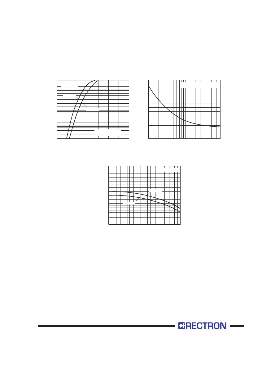
INSTANTANEOUS FORWARD VOLTAGE, (V)
1
1
3
2
5
10
20
IN
ST
AN
TA
NE
O
US
F
O
RW
AR
D
CU
RR
EN
T,
(A
)
1.0
0.3
0.1
0.03
0.01
3.0
10
20
10
5
50
100
2.5
2.0
1.5
1.0
0.5
0
3.0
3.5
RATING AND CHARACTERISTICS CURVES ( SE1 THRU SE6 )
FIG.4 TYPICAL INSTANTANEOUS FORWARD
CHARACTERISTICS
FIG.5 MAXIMUM NON-REPETITIVE FORWARD
SURGE CURRENT
REVERSE VOLTAGE, (V)
JU
NC
TI
O
N
CA
PA
CI
TA
NC
E,
(p
F)
4
6
40
20
10
60
200
100
0.2
0.1
2
1
0.4
2
1.0
4
10
20
40
100
FIG.6 TYPICAL JUNCTION CAPACITANCE
8.3ms Single Half Sine-Wave
(JEDED Method)
Pulse Width=300uS
1% Duty Cycle
T
J
= 25
O
C
T
J
= 25
O
C
SE1~SE4
SE1~SE4
SE5~SE6
SE5~SE6
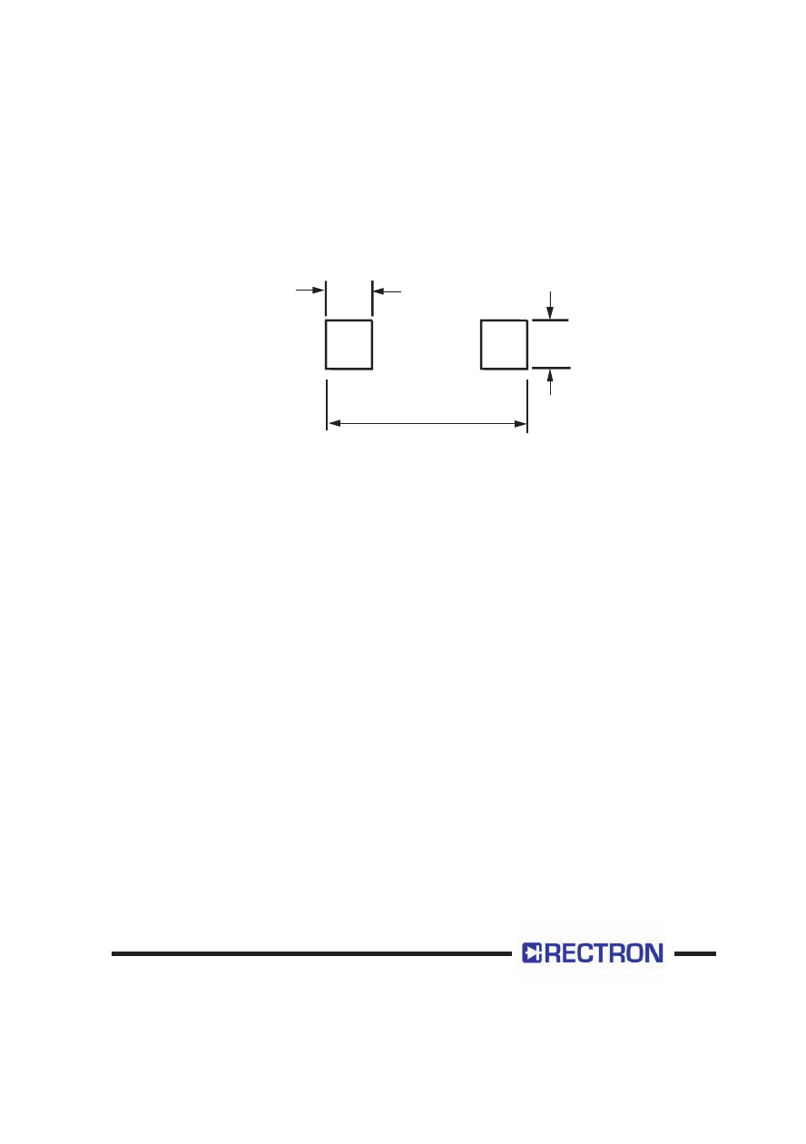
Mounting Pad Layout
Dimensions in inches and (millimeters)
0.035MIN.
(0.90 MIN.)
0.165
0.030 MIN.
(0.75 MIN.)
(4.19) REF

Rectron Inc reserves the right to make changes without notice to any product
specification herein, to make corrections, modifications, enhancements or other
changes. Rectron Inc or anyone on its behalf assumes no responsibility or liabi-
lity for any errors or inaccuracies. Data sheet specifications and its information
contained are intended to provide a product description only. "Typical" paramet-
ers which may be included on RECTRON data sheets and/ or specifications ca-
n and do vary in different applications and actual performance may vary over ti-
me. Rectron Inc does not assume any liability arising out of the application or
use of any product or circuit.
Rectron products are not designed, intended or authorized for use in medical,
life-saving implant or other applications intended for life-sustaining or other rela-
ted applications where a failure or malfunction of component or circuitry may di-
rectly or indirectly cause injury or threaten a life without expressed written appr-
oval of Rectron Inc. Customers using or selling Rectron components for use in
such applications do so at their own risk and shall agree to fully indemnify Rect-
ron Inc and its subsidiaries harmless against all claims, damages and expendit-
ures.
DISCLAIMER NOTICE