background image

SURFACE MOUNT

GLASS PASSIVATED  SILICON RECTIFIER

VOLTAGE  RANGE 50 to 1000 Volts  CURRENT 1.0 Ampere 

MAXIMUM RATINGS AND ELECTRICAL CHARACTERISTICS

Ratings at 25

O

C ambient temperature unless otherwise specfied.

Single phase, half wave, 60 Hz, resistive or inductive load.
For capacitive load, derate current by 20%.

SM4007

THRU

SM4001

MAXIMUM RATINGS 

(@ T

A

=25

O

C unless otherwise noted)

ELECTRICAL CHARACTERISTICS 

(@T

A

=25

O

C unless otherwise noted)

RATINGS

Maximum Recurrent Peak Reverse Voltage
Maximum RMS Voltage
Maximum DC Blocking Voltage
Maximum Average Forward Rectified Current

at Ambient Temperatur e
Peak Forward Surge Current 8.3 ms single half sine-wave

superimposed on rated load (JEDEC method)
Typical Thermal Resistance (Note 1)

Typical Junction Capacitance (Note 2)

SYMBOL

V

RRM

V

DC

I

FSM

C

J

 T

STG

V

RMS

UNITS

Volts

Volts

Volts

Amps

1.0

30

50

15

Amps

0

C/W

0

C/W

0

C

Storage Temperature Range

R

q

J A

Typical Thermal Resistance (Note 1)

20

R

q

J C

I

O

pF

Operating Temperature Range

T

J

SM4001

50

150

-55 to + 150

0

C

SM4002

SM4003

SM4004

SM4005

SM4006

100

200

400

600

35

70

140

280

420

50

100

200

400

600

SM4007

SM4001

SM4002

SM4003

SM4004

SM4005

SM4006

SM4007

800

1000

800

1000

560

700

2007-3

CHARACTERISTICS

Maximum Average Reverse Current
at Rated DC Blocking Voltage

V

F

SYMBOL

I

R

uA

Maximum Instantaneous Forward Voltage at 1.0A DC

Volts

5.0

100

@T

= 25

o

C

@T

= 100

o

C

uA

UNITS

1.1

NOTES : 1. Thermal Resistance :Mounted on PCB.

2. Measured at 1 MHz and applied reverse voltage of 4.0 volts.
3. "Fully ROHS compliant","100% Sn plating (Pb-free)". 

FEATURES

* Glass passivated device
* Ideal for surface mounted applications
* Low leakage current
* Metallurgically bonded construction
* Mounting position: Any
* Weight: 0.015 gram 

* Epoxy : Device has UL flammability classification 94V-0
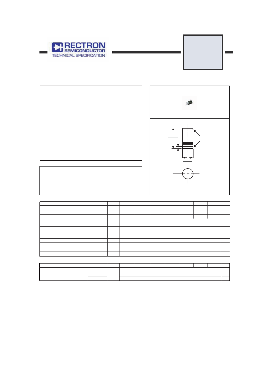
MECHANICA

DISCONTINUED-

L DATA

MELF

Dimensions in inches and (millimeters)

.205 ( 5.2 )

.190 ( 4.8 )

.024 ( 0.6 )

.016 ( 0.4 )

.106 ( 2.7 )

.095 ( 2.4 )

SOLDERABLE

ENDS

Disc

onti

nue

d

"This series is replaced by the FM400X series that meets to the same

fit and function parameters and share the same solder pad layout.

The FM400X series is preferred for error-free vacuum pick-up and

PCB assembly.

sm4001-sm4007-html.html
background image

PERCENT OF RATED PEAK REVERSE VOLTAGE,  (%)

INSTANTANEOUS  FORWARD VOLTAGE,  (V)

( ,

TN

ER

RU

DR

A

WR

OF 

SU

OE

NA

TN

AT

SNI

m

)A

AMBIENT TEMPERATURE, (

O

C)

0

0.01

1.0

0.1

10

100

1000

)A(

 ,

TN

ER

RU

DR

A

WR

OF 

E

GA

RE

VA

C

J

)F

p( ,

EC

NA

TI

CA

PA

N

OI

TC

NU

J ,

0

0.5

1.0

1.5

2.0

20

40

60

80

100

120

140

175

125

150

50

25

75

100

0

0

0.5 1.0

2.5

3.5 4.0 4.5

2.0

0.1

1.0

10

20

1.5

3.0

5.0

RATING AND CHARACTERISTICS CURVES ( SM4001 THRU SM4007 ) 

FIG.3 TYPICAL INSTANTANEOUS  FORWARD

FIG.3 TYPICAL INSTANTANEOUS  FORWARD

              CHARACTERISTICS

              CHARACTERISTICS

FIG.1 TYPICAL FORWARD CURRENT

FIG.1 TYPICAL FORWARD CURRENT

           DERATING CURVE

           DERATING CURVE

FIG.2 TYPICAL REVERSE

FIG.2 TYPICAL REVERSE

   CHARACTERISTICS

   CHARACTERISTICS

REVERSE VOLTAGE,  (V)

)A(

 ,

TN

ER

RU

ES

RE

VE

SU

OE

NA

TN

AT

SNI

0.1

1

8

6

4

2

10

20

40

40

0.4 1.0

4

10

80

FIG.4 TYPICAL JUNCTION CAPACITANCE 

FIG.4 TYPICAL JUNCTION CAPACITANCE 

NUMBER OF CYCLES AT 60Hz

)A(

 ,

TN

ER

RU

E

GR

US 

DR

A

WR

OF 

 K

AE

P

1

10

0

15

25

30

20

2

4

6 8 10

20

40

80 100

FIG.5 MAXIMUM NON-REPETITIVE FORWARD

FIG.5 MAXIMUM NON-REPETITIVE FORWARD

                SURGE CURRENT

                SURGE CURRENT

Single Phase Half Wave 60Hz

Resistive or Inductive Load

0.375" (9.5mm) Lead Length

T

J

 = 25 

O

C

Pulse width=300 S

1% Duty Cycle

T

J

 = 25 

O

C

8.3mS Single Half Sine-Wave

JEDEC Method

T

A

 = 25 

O

C

T

A

 = 75 

O

C

T

A

 = 100 

O

C

sm4001-sm4007-html.html
background image

Mounting Pad Layout

Dimensions in inches and (millimeters)


.100 (2.54)

.200 (5.08)

.300 (7.62)

.100 (2.54)

.100 (2.54)

F-SLOT WIDTH
OPTIMUM PAD SIZE

sm4001-sm4007-html.html
background image


                 Rectron Inc reserves the right to make changes without notice to any product 

              specification herein, to make corrections, modifications, enhancements or other 

              changes. Rectron Inc or anyone on its behalf assumes no responsibility or liabi-

              lity for any errors or inaccuracies.  Data sheet specifications and its information 

              contained are intended to provide a product description only. "Typical" paramet-

              ers which may be included on RECTRON data sheets and/ or specifications ca-

              n and do vary in different applications and actual performance may vary over ti-

              me.  Rectron Inc does not assume any liability arising out of the application or 

              use of any product or circuit.  

                 Rectron products are not designed, intended or authorized for use in medical,

              life-saving implant or other applications intended for life-sustaining or other rela-

              ted applications where a failure or malfunction of component or circuitry may di-

              rectly or indirectly cause injury or threaten a life without expressed written appr-

              oval of Rectron Inc.  Customers using or selling Rectron components for use in 

              such applications do so at their own risk and shall agree to fully indemnify Rect-

              ron Inc and its subsidiaries harmless against all claims, damages and expendit-

              ures.  

DISCLAIMER NOTICE