Walsin Technology Corporation
for CHIP-R and MLCC
Soldering Joint Criteria
Page 2
Screen or Stencil Printing of Solder Paste
Placement Accuracy
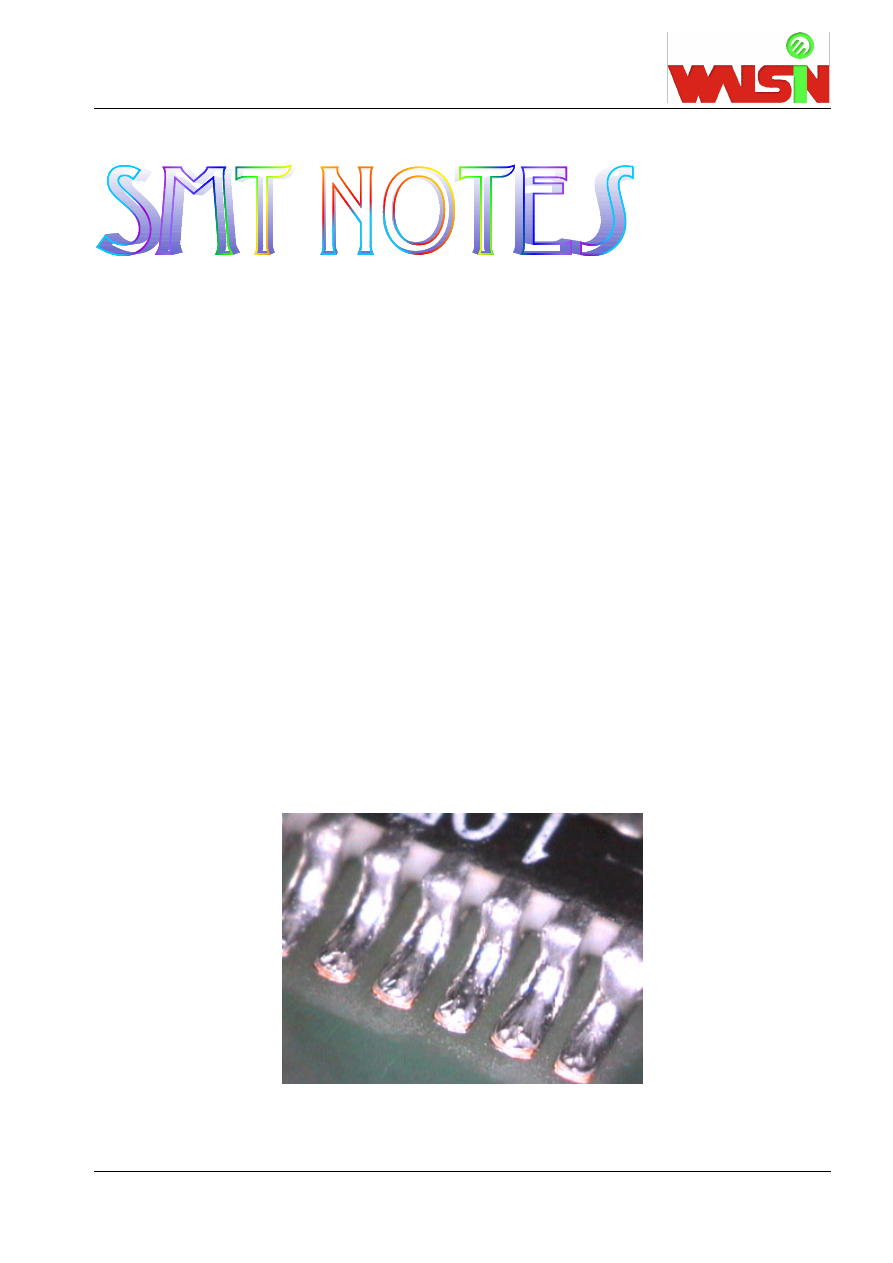
Visual inspection of soldered joints
Guidelines for Footprint Design
Page 7
Footprint design for Discrete CHIP-R / 8P4R Array Resistor
Footprint design for 10P8R network Resistor
Footprint design for Discrete MLCC / 8P4CArray Capacitor
Stencil thickness
Reflow soldering
Page 11
Wave soldering
Page 14
Adhesive and Adhesive Application
Page 16
PCB design guidelines
Page 18
Precaution of handling
Page 21
Surface Mounted Technology Notes
Page
1
2002a