Ceramic Surface Mount
Mounting Pad
Dimensions and Considerations
The objective of this document is to introduce the IPC-SM-782 methodology for
solder reflow land patterns. The methodology will be extended to all NOVACAP
standard and non-standard part sizes including assumptions for pick & place
accuracy along with desired solder fillets. NOVACAP strongly recommends the
user review the IPC-SM-782 document and visit their web site at
www.ipc.org
.
We remind the user they are responsible for all additional modifications needed
for solder fillet visual requirements and level of robustness.
The amount of solder applied to the chip capacitor will influence the reliability of
the device. Excessive solder can create thermal and tensile stresses on the
component that could lead to fracturing of the chip or the solder joint itself.
Insufficient or uneven solder application can result in weak bonds, rotation of the
device off line or lifting of one terminal off the pad (tombstoning).
The volume of solder is process and board pad size dependent. The following
pad sizes are represented for solder reflow and vapor phase processes. WAVE
SOLDERING exposes the devices to a large solder volume, hence the pad size
area must be restricted to accept an amount of solder that is not detrimental to
the chip size utilized. Typically the pad width is 66% of the component width, and
the length is .030 (.760 mm) longer than the termination band on the chip. A
0805 chip, which is .050 wide and has a .020 termination band, therefore
requires a pad .033 wide by .050 in length. Opposing pads should be identical in
size to preclude uneven solder fillets and mismatched surface tension forces,
which can misalign the device. It is preferred that the pad layout results in
alignment of the long axis of the chips at right angles to the solder wave, to
promote even wetting of all terminals. Orientation of components in line with the
board travel direction may require dual waves with solder turbulence to preclude
cold solder
25111

joints on the trailing terminals of the devices, as these are blocked from full
exposure to the solder by the body of the capacitor. Restrictions in chip
alignment do not apply to SOLDER REFLOW or VAPOR PHASE processes,
where the solder volume is controlled by the solder paste deposition on the
circuit pads. Pads are designed to match or slightly exceed the width of the
capacitor, with length .030 (.760 mm) greater than the chip terminal band width,
to provide a wetting area for a full solder fillet.
Most of the ceramic surface mount capacitors may not be wave soldered. The
0402 size capacitors will likely experience solder bridging due to the close
proximity of the terminations. The 0603 can be wave soldered however the glue
dots must be accurately placed and the wave controlled to prevent bridging.
Ceramic capacitors larger than 1210 should not be wave soldered. Large
thermal gradients are present as well as robustness issues due to board flex
problems. Some design layouts have required wave soldering of the 1812 size.
This should be done with extreme caution.
There are practical limitations on capacitor sizes that prohibit reliable direct
mounting of chip capacitors larger than 2225 to a substrate. Without mechanical
restriction, thermally induced stresses are released once the capacitor attains a
steady state condition, at any given temperature. Capacitors bonded to
substrates, however, will retain some stress, due primarily to the mismatch of
expansion of the component to the substrate; the residual stress on the chip is
also influenced by the ductility and hence the ability of the bonding medium to
relieve the stress. Unfortunately, the thermal expansions of chip capacitors differ
significantly from those of substrate materials. At 25°C to 300°C, capacitors
typically range in expansion coefficient from 8.3 x 10
-6
to 12.2 x 10
-6
in/in/°C,
while 99% Alumina is approximately 6.0 x 10
-6
in/in/°C and P.C. board is typically
16.0 x 10
-6
in/in/°C.
The IPC-SM-782 formulas and calculation were adopted to determine the pad
sizes for the “J” and “L” leaded configurations. An industry standard does not
exist for these leaded configurations. The tab dimension and tolerances
replacing the endband numbers determined the dimensions. The capacitor
thickness range was remained constant at .010”-.070” for the toe, heel, and side
solder fillet calculations.
All statements, information and data given within this document are believed to
be accurate and reliable, but are presented without guarantee, warranty, or
responsibility of any kind, expressed or implied. Specifications are typical and
may not apply to all applications.
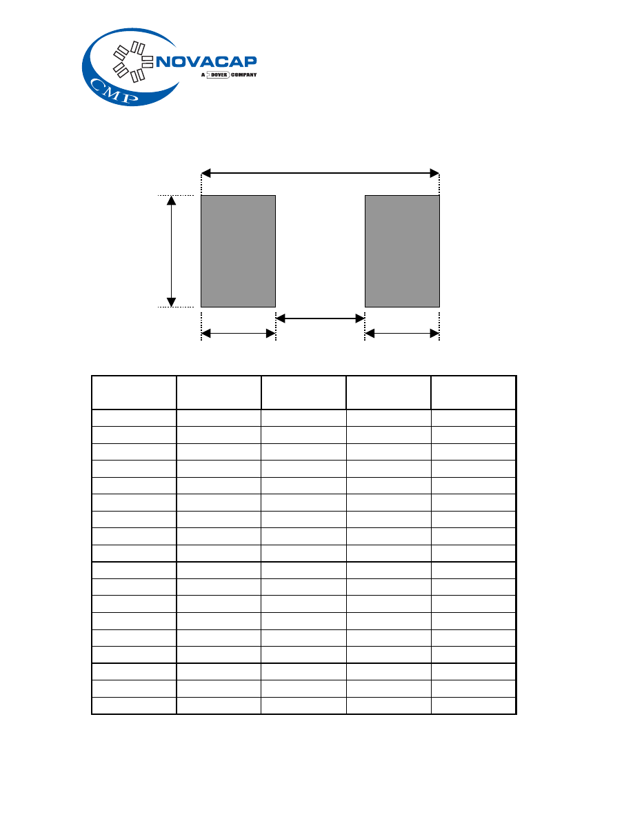
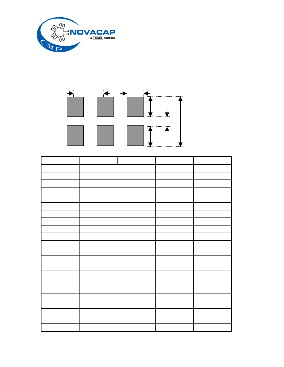
Footprint Design For Surface Mount Capacitors
D
A
C
B B
SIZE
A
B
C
D
Width
Pad
Spacing
Length
0402
0.028
0.035
0.018
0.088
0403
0.038
0.035
0.018
0.088
0504
0.048
0.036
0.026
0.098
0603
0.038
0.040
0.030
0.110
0805
0.060
0.045
0.035
0.125
1005
0.060
0.055
0.040
0.150
1206
0.068
0.065
0.045
0.175
1209
0.100
0.065
0.045
0.175
1210
0.110
0.065
0.045
0.175
1515
0.165
0.070
0.060
0.200
1808
0.090
0.075
0.080
0.230
1812
0.135
0.075
0.080
0.230
1825
0.265
0.075
0.080
0.230
2020
0.215
0.075
0.100
0.250
2211
0.120
0.085
0.105
0.275
2215
0.160
0.085
0.105
0.275
2221
0.225
0.085
0.105
0.275
2225
0.265
0.085
0.105
0.275
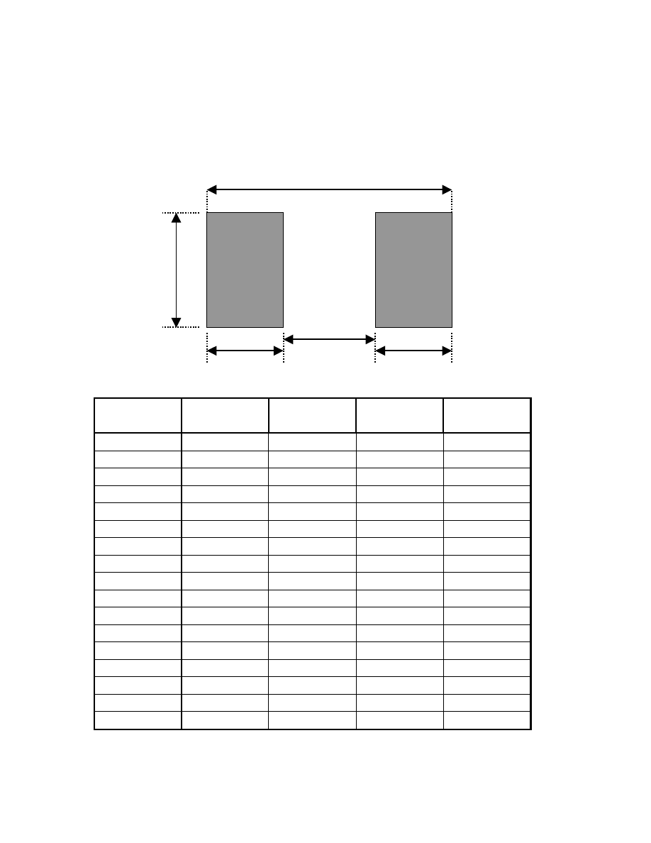
Footprint Design For Large Surface Mount Capacitors
(NOVACAP does not recommend direct mounting of chip capacitors larger
than 2225 to a substrate. Pad sizes are presented to satisfy requests. Care
must be taken in use for differences of thermal expansion.)
D
A
C
B B
SIZE
A
B
C
D
Width
Pad
Spacing
Length
2520
0.215 0.085 0.130 0.300
3030
0.315 0.085 0.180 0.350
3040
0.420 0.085 0.180 0.350
3333
0.350 0.090 0.210 0.390
3520
0.215 0.090 0.230 0.410
3530
0.315 0.090 0.230 0.410
3540
0.420 0.090 0.230 0.410
3545
0.475 0.090 0.230 0.410
3640
0.420 0.090 0.240 0.420
4020
0.215 0.105 0.250 0.460
4040
0.420 0.105 0.250 0.460
4540
0.420 0.105 0.300 0.510
5040
0.420 0.110 0.345 0.565
5440
0.420 0.110 0.390 0.610
5550
0.525 0.110 0.400 0.620
6560
0.630 0.115 0.490 0.720
7565
0.685 0.120 0.590 0.830
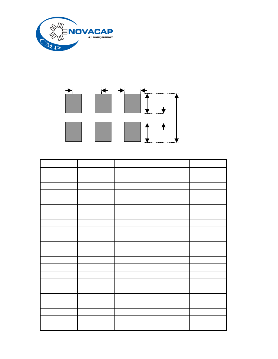
Footprint Design for “J” leaded Capacitors
.100” Typ. .040” Typ
B
C D
B
Size
# Leads
B
C
D
1812
2
0.100
0.050
0.250
1825
3
0.100
0.050
0.250
2020
2
0.100
0.070
0.270
2221
2
0.105
0.085
0.295
2225
3
0.105
0.085
0.295
2520
2
0.105
0.115
0.325
3030
3
0.105
0.165
0.375
3040
4
0.105
0.165
0.375
3333
3
0.110
0.185
0.405
3520
2
0.110
0.205
0.425
3530
3
0.110
0.205
0.425
3540
4
0.110
0.205
0.425
3545
5
0.110
0.205
0.425
3640
4
0.110
0.215
0.435
4020
2
0.110
0.260
0.480
4040
4
0.110
0.260
0.480
4540
4
0.115
0.300
0.530
5040
4
0.115
0.355
0.585
5440
4
0.115
0.395
0.625
5550
5
0.120
0.395
0.635
6560
6
0.120
0.500
0.740
7565
6
0.125
0.595
0.845
Footprint Design for “L” leaded Capacitors
.100” Typ. .040” Typ
B
C D
B
Size
# Leads
B
C
D
1812
2
0.100
0.150
0.350
1825
3
0.100
0.150
0.350
2020
2
0.100
0.170
0.370
2221
2
0.105
0.185
0.395
2225
3
0.105
0.185
0.395
2520
2
0.105
0.215
0.425
3030
3
0.105
0.265
0.475
3040
4
0.105
0.265
0.475
3333
3
0.110
0.285
0.505
3520
2
0.110
0.305
0.525
3530
3
0.110
0.305
0.525
3540
4
0.110
0.305
0.525
3545
5
0.110
0.305
0.525
3640
4
0.110
0.315
0.535
4020
2
0.110
0.360
0.580
4040
4
0.110
0.360
0.580
4540
4
0.115
0.400
0.630
5040
4
0.115
0.455
0.685
5440
4
0.115
0.495
0.725
5550
5
0.120
0.495
0.735
6560
6
0.120
0.600
0.840
7565
6
0.125
0.695
0.945