SURFACE MOUNT GLASS PASSIVATED
SUPER FAST SILICON RECTIFIER
VOLTAGE RANGE 50 to 200 Volts CURRENT 2.0 Amperes
MAXIMUM RATINGS AND ELECTRICAL CHARACTERISTICS
Ratings at 25
o
C ambient temperature unless otherwise specified.
Single phase, half wave, 60 Hz, resistive or inductive load.
For capacitive load, derate current by 20%.
UFM204L
THRU
UFM201L
SMBL
MAXIMUM RATINGS
(@ T
A
=25
O
C unless otherwise noted)
ELECTRICAL CHARACTERISTICS
(@T
A
=25
O
C unless otherwise noted)
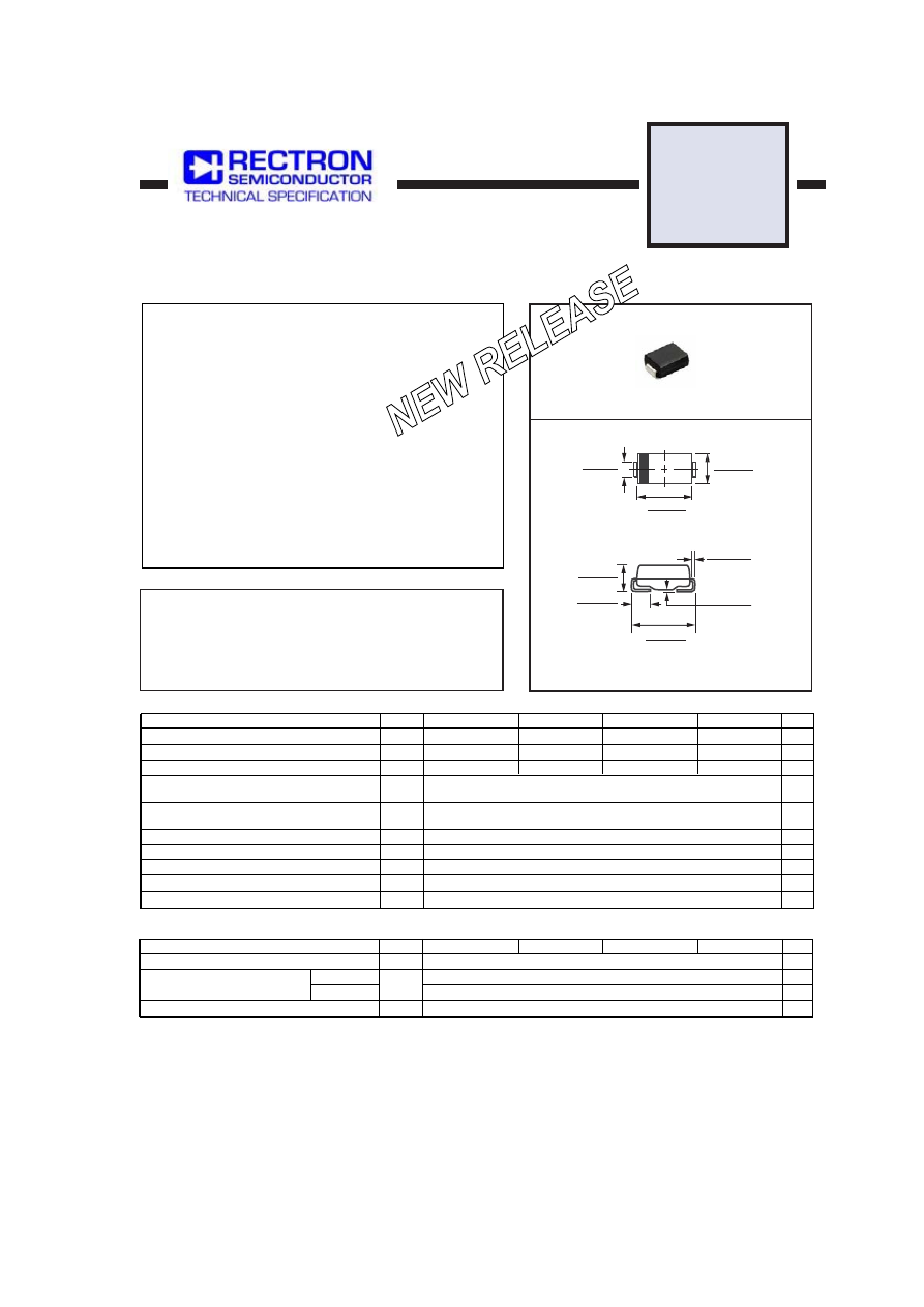
Dimensions in inches and (millimeters)
RATINGS
Maximum Recurrent Peak Reverse Voltage
Maximum RMS Voltage
Maximum DC Blocking Voltage
Maximum Average Forward Rectified Current
at T
A
= 55
O
C
Peak Forward Surge Current 8.3 ms single half sine-wave
superimposed on rated load (JEDEC method)
Typical Thermal Resistance (Note 1)
Typical Junction Capacitance (Note 2)
SYMBOL
V
RRM
V
DC
I
FSM
C
J
T
STG
V
RMS
UNITS
Volts
Volts
Volts
Amps
2.0
50
75
18
Amps
0
C/W
0
C/W
0
C
Storage Temperature Range
R
q
J A
Typical Thermal Resistance (Note 1)
20
R
q
J L
I
O
pF
Operating Temperature Range
T
J
UFM201L
50
150
-55 to + 150
0
C
UFM202L
UFM203L
100
150
35
70
105
50
100
150
UFM204L
UFM201L
UFM202L
UFM203L
UFM204L
200
200
140
2006-12
CHARACTERISTICS
Maximum Average Reverse Current
at Rated DC Blocking Voltage
V
F
SYMBOL
I
R
m
A
Maximum Instantaneous Forward Voltage at 2.0A DC
Volts
5
350
@T
A
= 25
o
C
@T
A
= 100
o
C
m
A
UNITS
0.9
trr
Maximum Reverse Recovery Time (Note 4)
nSec
20
FEATURES
* Glass passivated device
* For surface mounted applications
* Ultrafast recovery times dor high efficiency
* Low forward voltage, low power loss
* Low leakage current
* Epoxy: Device has UL flammability classification 94V-O
* Metallurgically bonded construction
* Mounting position: Any
* Weight: 0.098 gram
0.083 (2.11)
0.077 (1.96)
0.155 (3.94)
0.130 (3.30)
0.180 (4.57)
0.160 (4.06)
0.085 (2.15)
0.061 (1.55)
0.060 (1.52)
0.030 (0.76)
0.220 (5.59)
0.205 (5.21)
0.012 (0.305)
0.006 (0.152)
0.008 (0.203)
0.004 (0.102)
MECHANICAL DATA
NOTES : 1. Thermal Resistance :Mounted on PCB.
2. Measured at 1 MHz and applied reverse voltage of 4.0 volts.
3. "Fully ROHS compliant","100% Sn plating (Pb-free)".
4. Test Conditions: I
F
= 0.5A, I
R
= -1.0A, I
RR
= -0.25A.