PH10 TECHNOLOGY
Build your own solution with UMS
The UMS 0.1
µ
m GaAs Very High Frequency
pHEMT Process
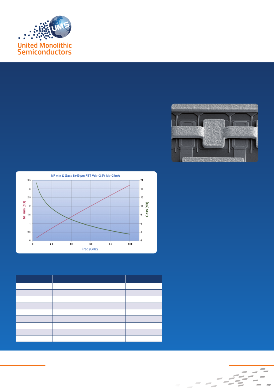
PH10 process is optimised for low noise amplification up
to 110GHz with a typical Ft of 130GHz, a power density
above 300mW/mm at 3V and a typical noise figure of
2.3dB @ 70GHz. It includes two metal interconnect layers,
precision TaN resistors, high values TiWSi resistors, MIM
capacitors, air-bridges, via-holes and gold plated back
side. PH10 is available with BCB encapsulation.
www.ums-rf.com
Process main characteristics
Element
Parameter
Typical Value
Condition
FET
Idss (mA/mm)
280
Vds=2.0V, Gm_max
Gm_max (mS/mm)
725
Vds=2.0V, Gm_max
Vbds (V)
6
Ids= Idss/100
Noise Figure (dB)
2.3
@ 70GHz
MIM Capacitor
Density (pF/mm2)
330
@ 1MHz
Resistor
TaN
30
Ohms/sq
TiWSI
1000
Ohms/sq
GaAs
120
Ohms/sq
Substrate
Thickness
70
µm
PH10 offers a very wide
range of applications
among them:
• E-Band point-to-point
communication
• W-Band radar
• Fiber Optics
• Security sensors
• Space instrumentation
• …
Typical UMS product
references are:
• LNA 71-86GHz: CHA2080-98F
• MPA 71-76GHz: CHA3080-98F
• MPA 81-86GHz: CHA3090-98F
• Down-converter CHR1080a98F