GaN TECHNOLOGY
GH15 GaN process is optimized for applications up to 40GHz
for high power, high PAE and high linearity.
Supported by a thermally dissipative SiC substrate, the power density reaches
4.2W/mm. This MMIC process includes MIM capacitors, inductors, air
bridges, metallic resistors, via through the substrate and two metal layers for
interconnections.
GH15 is the ideal process
to design:
• High power and high PAE amplifiers
up to 40GHz
• Robust LNA
• High Power switches
Build your own solution with UMS
www.ums-rf.com
0.15µm
GaN HEMT
process
>>>
Industrial technologies
qualified for
Space
UMS 2024/2025
- Printed on PEFC paper - Smith Corporate : 01 69 59 1
1 30 - www
.smithcorporate.fr
Contact us:
Worldwide distributor:
Richardson RFPD
www.richardsonrfpd.com
UMS SAS - EMEA
Ph: +33 1 69 86 32 00
mktsales@ums-rf.com
UMS USA Inc. - America
Ph: +1 781 791 5078
philippe.labasse@ums-rf.com
UMS - Asia
Ph: +65 9298 8316
thomas.vacher@ums-rf.com
www.ums-rf.com
Process Design Kits (PDK) will include non-linear electro-thermal models, noise model, diodes
& switches models, passive models, all with associated library elements.
Applications targeted
with GH15:
• Pt to Pt radio
• 5G
• Satcom
• Radar
• Broadband amplification
• Hi-Rel products
Element
Typical Value
Vt
-3,2 V
Power Density
4.2W/mm
Ids+
1.45 A/mm
Gm
405 mS/mm
VdsDC
Up to 25V
NF/Gass
1.5dB / 11dB @ 15GHz
Fmax
> 100 GHz
MIM density
175 pF/mm
2
(and 355 pF/mm
2
for GH15-11)
Metallic resistors
30 and 1000 Ohms/sq
Max freq use
40GHz
Process main features
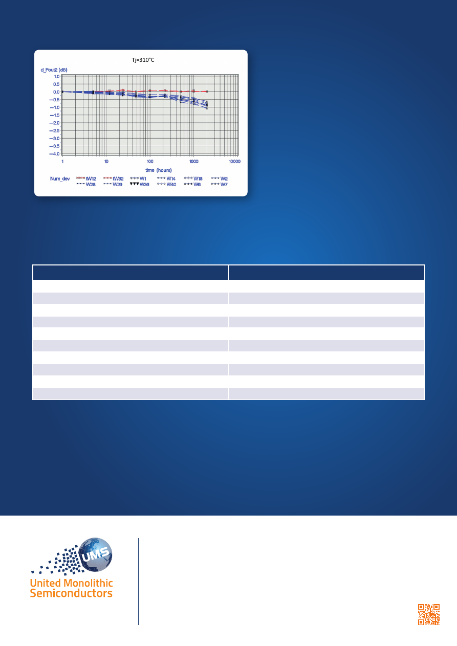
Proven reliability
GH15 is available in four technology versions:
• GH15-10, Space evaluated
• GH15-11, providing additional options, such as High Density MIM 355pF/mm2 and BCB
mechanical protection for compatibility with plastic molded packaging.
• GH15-12, providing mechanical and humidity protection
• GH15-13, with thinner substrate specially optimized for Q-band applications