background image

Rev. 1.3 (December 2009)                                           1                                              © DLP Design, Inc.


D

D

L

L

P

P

-

-

U

U

S

S

B

B

1

1

2

2

3

3

2

2

H

H


LEAD-FREE


H

H

I

I

G

G

H

H

-

-

S

S

P

P

E

E

E

E

D

D


U

U

S

S

B

B


A

A

D

D

A

A

P

P

T

T

E

E

R

R


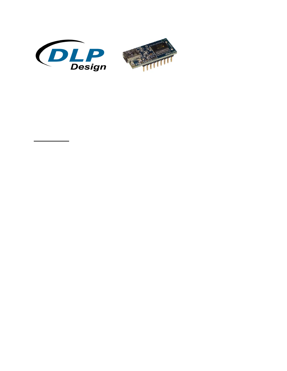
The DLP-USB1232H is DLP Design’s premier USB-to-UART/FIFO interface module

 based on 

FTDI’s 5

th 

generation USB 2.0 High Speed (480Mb/s) silicon

.  The DLP-

USB1232H is available in a lead-free, RoHS-compliant, compact 18-pin, 0.1-inch spaced 
standard DIP footprint. 
 

FEATURES: 

 
The DLP-USB1232H has the capability of being configured in a variety of 
industry standard serial or parallel interfaces supporting these features: 
 

• Entire USB protocol handled on the module. No USB specific firmware programming required. 
• USB 2.0 High Speed (480Mbits/Second) and Full Speed (12Mbits/Second) compatible. 
• Multi-Protocol Synchronous Serial Engine (MPSSE) to simplify synchronous serial protocol 
(USB to JTAG, I2C, SPI or bit-bang) design. 
• RS232/RS422/RS485 UART Transfer Data Rate up to 12Mbaud. (RS232 Data Rate limited by 
external level shifter). 
• USB to parallel FIFO transfer data rate up to 8 Mbyte/Sec. 
• CPU-style FIFO interface mode simplifies CPU interface design. 
• FTDI’s royalty-free Virtual Com Port (VCP) and Direct (D2XX) drivers eliminate the 
requirement for USB driver development in most cases. 
• Adjustable receive buffer timeout. 
• Transmit and receive LED drive signals. 
• FT245B-style FIFO interface option with bidirectional data bus and simple 4 wire 
handshake interface. 
• Asynchronous serial UART interface option with full hardware handshaking and modem 
interface signals. 
• Fully assisted hardware or X-On / X-Off software handshaking. 
• UART Interface supports 7/8 bit data, 1/2 stop bits, and Odd/Even/Mark/Space/No Parity. 
• Auto-transmit enable control for RS485 serial applications using TXDEN pin. 
• Operational configuration mode and USB Description strings configurable in on-boardl 
EEPROM over the USB interface. 
• Configurable I/O drive strength (4, 8, 12 or 16mA) and slew rate. 
• Low operating and USB suspend current. 
• Supports bus powered, self powered and high-power bus powered USB configurations. 
• UHCI/OHCI/EHCI host controller compatible. 
• USB Bulk data transfer mode (512 byte packets in High Speed mode). 
• +3.3V I/O interfacing (+5V Tolerant). 
• Extended -40°C to 85°C industrial operating temperature range. 

usb1232h-ds-v13-html.html
background image

Rev. 1.3 (December 2009)                                           2                                              © DLP Design, Inc.


APPLICATION AREAS: 


• Upgrading legacy peripherals to USB 
• Interfacing MCU/PLD/FPGA-based designs to USB 
• USB to UART (RS232, RS422 or RS485) 
• USB to FIFO 
• USB to JTAG 
• USB to SPI 
• USB to I2C 
• USB to Bit-Bang 
• USB to CPU target interface (as memory) 
• PDA to USB data transfer 
• USB Smart Card Readers 
• USB Instrumentation 
• USB Industrial Control 
• USB MP3 Player Interface 
• USB FLASH Card Reader / Writers 
• Set Top Box PC - USB interface 
• USB Digital Camera Interface 
• USB Bar Code Readers 
• USB audio and low-bandwidth video data transfer 
• USB hardware modems 
• USB wireless modems 
 

DRIVER SUPPORT: 


Royalty-Free Virtual COM Port (VCP) Drivers for: 

 
• Windows 2000, Server 2003, Server 2008 
• Windows XP and XP 64-bit 
• Windows Vista and Vista 64-bit 
• Windows XP Embedded 
• Windows CE 4.2, 5.0, 5.2 and 6.0 
• Mac OS-X 
• Linux 2.6.9 or later 
 

Royalty-Free D2XX Direct Drivers (USB Drivers + DLL S/W Interface) for:


• Windows 2000, Server 2003, Server 2008 
• Windows XP and XP 64-bit 
• Windows Vista and Vista 64-bit 
• Windows XP Embedded 
• Windows CE 4.2, 5.0, 5.2 and 6.0 
• Linux 2.4 or later and Linux x86_64  
 
The drivers listed above are all available for free download from the DLP Design website 

www.dlpdesign.com

 and FTDI website 

www.ftdichip.com

 
Various third-party drivers are also available for other operating systems; see the FTDI website 

www.ftdichip.com

 for details. 

usb1232h-ds-v13-html.html
background image

Rev. 1.3 (December 2009)                                           3                                              © DLP Design, Inc.


ABSOLUTE MAXIMUM RATINGS 


• 

Storage 

Temperature     -65°C 

to 

+150°C 

• Ambient Temperature (Power Applied)  


-40 to +85°C 

• VCC Supply Voltage  


-0.5V to +6.00V 

• DC Input Voltage:  Inputs    


-0.5V to VCC + 0.5V 

• DC Input Voltage:  High-Impedance Bidirectionals  

-0.5V to VCC + 0.5V 

• DC Output Current:  Outputs  


16mA 


D.C. CHARACTERISTICS (AMBIENT TEMPERATURE:  -40 TO 85°C) 


• VCC Operating-Supply Voltage 


4.0 - 5.5V 

• VCCIO Digital IO Voltage 


3.3V 

• Operating Supply Current   


75mA (Normal Operation) 

• 

Operating 

Supply 

Current 

    500uA 

USB 

Suspend 


1.0  GENERAL DESCRIPTION 


The DLP-USB1232H USB 2.0 High Speed (480Mb/s) to UART/FIFO uses FTDI’s 5th generation 
USB silicon. It has the capability of being configured in a variety of industry standard serial or 
parallel interfaces. The DLP-USB1232H can be configured for UART, FIFO, JTAG, SPI, I2C or 
bit-bang mode. In addition to these, the DLP-USB1232H supports a CPU interface FIFO mode. 
 
Refer to the FT2232H datasheet for additional detail on how to set up and use the supported 
modes. 


usb1232h-ds-v13-html.html
background image

Rev. 1.3 (December 2009)                                           4                                              © DLP Design, Inc.


2.0 PIN DESCRIPTIONS 

 
This section describes the operation of the DLP-USB1232H pins.  The function of the I/O pins is 
determined by the configuration that is stored in the EEPROM connected to the FT2232H USB 
IC. 
 
The following table details the function of each pin for the specified mode.  Note that the 
convention used throughout this document for active low signals is the signal name followed by 
a #.  Pins marked ** default to tri-stated inputs with an internal 75K Ohm (approx) pull up 
resistor to VCCIO (3.3V). 


DLP-USB1232H 

Pin 

Pin Functions For Each Supported Mode 

Pin # 

Pin Name 

ASYNC 

Serial 

(RS232) 

245 FIFO 

ASYNC 

Bit-bang 

SYNC 

Bit-bang 

MPSSE 

CPU 

Target 

Channel A 

18 ADBUS0 TXD 

D0 

D0 

D0 TCK/SK D0 

16 ADBUS1 RXD 

D1 

D1 

D1  TDI/DO D1 

2 ADBUS2 

RTS# 

D2 

D2 

D2 TDO/DI D2 

5 ADBUS3 

CTS# 

D3 

D3 

D3 TMS/CS D3 

17 ADBUS4 DTR# 

D4 

D4 

D4 GPIOL0 D4 

4 ADBUS5 

DSR# 

D5 

D5 

D5 GPIOL1 D5 

13 ADBUS6 DCD# 

D6 

D6 

D6 GPIOL2 D6 

3 ADBUS7 RI# 

D7 

D7 

D7 GPIOL3 D7 

15 ACBUS0 

TXDEN  RXF# 

** 

**  GPIOH0 CS# 

14 ACBUS1   

TXE# 

WRSTB# WRSTB# 

GPIOH1 A0 

11 ACBUS2   

RD# 

RDSTB#  RDSTB# 

GPIOH2 

RD# 

12 ACBUS3 

TXLED#  WR# 

** 

**  GPIOH3 

WR# 

7 ACBUS4 

RXLED# SIWUA 

SIWUA  SIWUA 

GPIOH4 

SIWUA 

usb1232h-ds-v13-html.html
background image

Rev. 1.3 (December 2009)                                           5                                              © DLP Design, Inc.


2.0  TIMING DIAGRAMS - 245 FIFO MODE 


T

T

I

I

M

M

E

E


D

D

E

E

S

S

C

C

R

R

I

I

P

P

T

T

I

I

O

O

N

N


M

M

I

I

N

M

M

A

A

X

X


U

U

N

N

I

I

T

T1 

RD# Active Pulse Width 

50 - 

nS 

T2 

RD# to RD# Pre-Charge  

T5 + T6 

nS 

T3 

RD# Active to Valid Data* 

20 50 

nS 

T4 

Valid Data Hold Time from RD# Inactive* 

0 - 

nS 

T5 

RD# Inactive to RXF# output active 

0 25 

nS 

T6 

RXF# Inactive After RD Cycle 

33 67 

nS 


         *Load = 30pF 


T

T

I

I

M

M

E

E


D

D

E

E

S

S

C

C

R

R

I

I

P

P

T

T

I

I

O

O

N

N


M

M

I

I

N

M

M

A

A

X

X


U

U

N

N

I

I

T

T7 

WR Active Pulse Width 

10 - 

nS 

T8 

WR to WR Pre-Charge Time 

50 - 

nS 

T9 

Valid Data Setup to WR Falling Edge* 

20 - 

nS 

T10 

Valid Data Hold Time from WR Inactive* 

10 - 

nS 

T11 

WR Inactive to TXE# 

10 25 

nS 

T12 

TXE# Inactive After WR Cycle 

49 84 

nS 


         *Load = 30pF 


       T6 


T5


   RXF# 


    T1  


       T2 

     RD# 


               T3                                 


  T4


 Description Min Max Unit 


Valid data 

D[7 ..0] 


Valid data

D[7 ..0] 

T 10

T 9

TXE# 

WR 

T11 

T12

T7

T8 

usb1232h-ds-v13-html.html
background image

Rev. 1.3 (December 2009)                                           6                                              © DLP Design, Inc.


3.0  APPLICATION NOTES 


USB devices transfer data in packets.  If data is to be sent from the PC, a packet is built up by 
the application program and is sent via the device driver to the USB scheduler.  This scheduler 
adds a request to the list of tasks that the USB host controller will perform.  This will typically 
take at least 1 millisecond to execute because it will not pick up the new request until the next 
USB frame (the frame period is 1 millisecond).  There is, therefore, sizeable overhead 
(depending upon your required throughput) associated with moving data from the application to 
the USB device.  If data is sent one byte at a time by an application, this will severely limit the 
overall throughput of the system. 
 
It must be stressed that in order to achieve maximum throughput, application programs should 
send or receive data using buffers and not individual characters. 


4.0  DRIVER SOFTWARE 


FTDI's VCP (Virtual COM Port) USB driver files are provided royalty free on the condition that 
they are only used with designs incorporating an FTDI device (i.e. the FT2232H and DLP-
USB1232H).  The latest version of the drivers can be downloaded from either 

www.dlpdesign.com

 or 

www.ftdichip.com

 
The CDM driver download file is a combined set of drivers for the Windows operating system 
and contains both the VCP and D2XX driver versions.  To download, simply unzip the file to a 
folder on your PC.  (The drivers can coexist on the same floppy disk or folder since the INF files 
determine which set of drivers to load for each operating-system version.)  Once loaded, the 
VCP drivers will allow your application software—running on the host PC—to communicate with 
the DLP-USB1232H as though it were connected to a COM (RS-232) port. 
 
In addition to VCP drivers, FTDI's D2XX direct drivers for Windows offer an alternative solution 
to the VCP drivers that allow application software to interface with the FT2232H device using a 
DLL instead of a Virtual COM Port.  The architecture of the D2XX drivers consists of a Windows 
WDM driver that communicates with the FT2232H device via the Windows USB stack and a 
DLL that interfaces with the application software (written in VC++, C++ Builder, Delphi, VB, etc.) 
to the WDM driver. 
 
The D2XX direct drivers add support for simultaneous access and control of multiple DLP-
USB1232H devices.  The extended open function (FT_OpenEx) allows the device to be opened 
either by its product description or serial number, both of which can be programmed to be 
unique.  The list devices function (FT_ListDevices) allows the application software to determine 
which devices are currently available for use, again by either product description or serial 
number.  
 
Download FTDI Application Notes AN_103 and AN_104 for detailed instructions on how to 
install the drivers on XP and Vista platforms. 


usb1232h-ds-v13-html.html
background image

Rev. 1.3 (December 2009)                                           7                                              © DLP Design, Inc.


5.0  EEPROM WRITE UTILITY 


The DLP-USB1232H has the option to accept manufacturer-specific information that is written 
into EEPROM memory.  Parameters that can be programmed include the VID and the PID 
identifiers, the manufacturer's product string and a serial number. 
 
MPROG is the latest EEPROM programming utility for the FT2232H device.  You must install 
the latest release of the CDM drivers in order to run this application.  If you have CDM drivers 
installed on the PC that is to perform the EEPROM write process, you can run MPROG and 
update the EEPROM contents with either mode (VCP or D2XX) active. 


6.0  QUICK START GUIDE 


This guide requires the use of a Windows XP/Vista PC that is equipped with a USB port. 

 
1.  Download the latest CDM device drivers from either 

www.dlpdesign.com

 or 

www.ftdichip.com

.  Unzip the drivers into a folder on the hard drive. 

 
2.  Connect the DLP-USB1232H module to the PC via a USB ‘A’ to mini-B cable. This action 

initiates the loading of the USB drivers.  When prompted, select the folder where the device 
drivers were stored in Step 1.  Windows will then complete the installation of the device 
drivers for the DLP-USB1232H module.  The next time the DLP-USB1232H module is 
attached, the host PC will immediately load the correct drivers without any prompting.  
Reboot the PC if prompted to do so. 

 
At this point, the DLP-USB1232H is ready for use.  Note that if the DLP-USB1232H is 
configured for 245 FIFO mode that it will appear non-responsive if data sent from the host PC is 
not read by an attached microcontroller, microprocessor, DSP, FPGA, ASIC, etc. 


7.0  PINOUT DESCRIPTION


USB

Pin 9

Pin 10

Top View

(Interface Headers on bottom of PCB)

Pin 1

Pin 18

usb1232h-ds-v13-html.html
background image

Rev. 1.3 (December 2009)                                           8                                              © DLP Design, Inc.


P

P

I

I

N

N


#

#


P

P

A

A

R

R

A

A

L

L

L

L

E

E

L

L


S

S

I

I

G

G

N

N

A

A

L

L


U

U

S

S

A

A

G

G

E

D

D

E

E

S

S

C

C

R

R

I

I

P

P

T

T

I

I

O

O

N

1 GROUND 

DB2

 - FIFO Data Bus Bit 2 

DB7

 - FIFO Data Bus Bit 7 

DB5

 - FIFO Data Bus Bit 5 

DB3

 - FIFO Data Bus Bit 3 

PWREN

 - 

Active low power-enable output. 

                  PWREN# = 0: Normal operation. 
                  PWREN# = 1: USB SUSPEND mode or device has not been configured. 
                  This can be used by external circuitry to power down logic when device is in USB 
                  suspend or has not been configured.

SIWUA

 -The Send Immediate / WakeUp signal combines two functions on a single pin. If 

USB is in suspend mode (PWREN# = 1) and remote wakeup is enabled in the EEPROM, 
strobing this pin low will cause the device to request a resume on the USB Bus.  
Normally, this can be used to wake up the Host PC.  During normal operation (PWREN# 
= 0), if this pin is strobed low any data in the device TX buffer will be sent out over USB 
on the next Bulk-IN request from the drivers regardless of the pending packet size. 
This can be used to optimize USB transfer speed for some applications. Tie this pin to 
VCCIO if not used.  

EXTVCC

 - Use for applying main power (4.5 to 5.25 volts) to the module.  Connect to 

PORTVCC (Pin 9) if the module is to be powered by the USB port (typical configuration). 

PORTVCC

 - Power from the USB port.  Connect to EXTVCC (Pin 8) if the module is to 

be powered by the USB port (typical configuration).  500mA is the maximum current 
available to the USB adapter and target electronics if the USB device is configured for 
high power. 

10 GROUND 

11 

RD#

 - When pulled low, RD# takes the 8 data lines from a high-impedance state to the 

current byte in the FIFO’s buffer. Taking RD# high returns the data pins to a high- 
impedance state and prepares the next byte (if available) in the FIFO to be read. 

12 

WR

 - When taken from a high to a low state, WR reads the 8 data lines and writes the 

byte into the FIFO’s transmit buffer.  Data written to the transmit buffer is sent to the host 
PC within the TX buffer timeout value (default 16mS) and placed in the buffer that was 
created when the USB port was opened.  The FT245R allows the TX buffer timeout value 
to be reprogrammed to a value between 1 and 255mS. 

13 

DB6

 - FIFO Data Bus Bit 6 

14 

TXE#

 - When high, do not write data into the FIFO.  When low, data can be written into 

the FIFO by strobing WR high, then low.  During reset this signal pin is tri-state.  Data is 
latched into the FIFO on the falling edge of the WR pin. 

15 

RXF#

 - When low, at least 1 byte is present in the FIFO’s receive buffer and is ready to 

be read with RD#.  RXF# goes high when the receive buffer is empty.  During reset this 
signal pin is tri-state.  If the Remote Wakeup option is enabled in the internal EEPROM, 
during USB Suspend Mode (PWREN#=1) RXF# becomes an input.  This can be used to 
wake up the USB host from Suspend Mode by strobing this pin low for a minimum of 
20ms which will cause the device to request a resume on the USB bus. 

16 

DB1

 - FIFO Data Bus Bit 1 

17 

DB4

 - FIFO Data Bus Bit 4 

18 

DB0 

- FIFO Data Bus Bit 0 


usb1232h-ds-v13-html.html
background image

Rev. 1.3 (December 2009)                                           9                                              © DLP Design, Inc.


P

P

I

I

N

N


#

#


S

S

E

E

R

R

I

I

A

A

L

L


S

S

I

I

G

G

N

N

A

A

L

L


U

U

S

S

A

A

G

G

E

E


D

D

E

E

S

S

C

C

R

R

I

I

P

P

T

T

I

I

O

O

N

1 GROUND 

RTS

 - Request to Send Control Output/Handshake Signal 

RI

 - Ring Indicator Control Input.  When remote wake-up is enabled in the internal 

EEPROM taking RI# low (20ms active low pulse), this can be used to resume the PC 
USB host controller from Suspend. 

DSR

 - Data Set Ready Control Input/Handshake Signal 

CTS

 - Clear To Send Control Input/Handshake Signal  

PWREN

 - 

Active low power-enable output. 

                  PWREN# = 0: Normal operation. 
                  PWREN# = 1: USB SUSPEND mode or device has not been configured. 
                  This can be used by external circuitry to power down logic when device is in USB 
                  suspend or has not been configured.

RXLED

 - 

Receive signaling output. Pulses low when receiving data via USB. This should be 

connected to an LED.


EXTVCC

 - Use for applying main power (4.5 to 5.25 volts) to the module.  Connect to 

PORTVCC (Pin 9) if the module is to be powered by the USB port (typical configuration). 

PORTVCC

 - Power from the USB port.  Connect to EXTVCC (Pin 8) if the module is to 

be powered by the USB port (typical configuration).  500mA is the maximum current 
available to the USB adapter and target electronics if the USB device is configured for 
high power. 

10 GROUND 
11 

RDSTB# 

-  

12 

TXLED#

 - 

Transmit signaling output. Pulses low when transmitting data via USB. This should be 

connected to an LED.


13 

DCD#

 - Data Carrier Detect Control Input 

14 

WRSTB#

  -  

15 

TXDEN

 - 

(TTL level). For use with RS485 level converters.


16 

RXD

 - Receiving Asynchronous Data Input 

17 

DTR#

 - Data Terminal Ready Control Output/Handshake Signal 

18 

TXD

 - Transmit Asynchronous Data Output 


usb1232h-ds-v13-html.html
background image

Rev. 1.3 (December 2009)                                           10                                              © DLP Design, Inc.


8.0  DEVICE CONFIGURATION EXAMPLES 


USB Bus-Powered and Self-Powered Configurations 


Figure 1. 


The figure above illustrates a typical USB bus-powered configuration.  A USB bus-powered 
device gets its power from the USB bus.   


Figure 2. 


Figure 2 illustrates a typical USB self-powered configuration.  A USB self-powered device gets 
its power from its own power supply and does not draw current from the USB bus.   


Figure 3. 


Figure 3 shows how to configure the DLP-USB1232H to interface with a microcontroller via the 
parallel 245 FIFO interface mode.  In this example, the target electronics can operate at from 
3.3 - 5 volts since the DLP-USB1232H interface I/O pins are 5 volt tolerant.  


9

7
8

Bus-Powered

5V System

9

7
8

Self-Powered

5V System

5.0V

Bus-Powered

5V System with

3.3V Logic Interface

8 Data Lines

3.3 - 5V

Microcontroller

9

7
8

WR

RXF#

RD#

TXE#

usb1232h-ds-v13-html.html
background image

Rev. 1.3 (December 2009)                                           11                                              © DLP Design, Inc.


Figure 4. 


Figure 4 shows how to configure the DLP-USB1232H to interface with a 3.3V logic device via 
the ASYNC serial mode.  In this example, the target electronics provide the 3.3 volts to power 
the microcontroller. 


9.0  BUS-POWERED CIRCUIT WITH POWER CONTROL 


USB bus-powered circuits need to be able to power down in USB Suspend Mode in order to 
meet the Suspend current requirement (including external logic): 


Figure 4. 


Figure 4 shows how to use a discrete P-Channel MOSFET to control the power to external logic 
circuits.  This “soft-start” circuit accommodates designs that draw more than 100mA at power 
up. 


PWREN#

Power Controlled by

PWREN#

Microcontroller

P-Channel

Power MOSFET

S

G

D

9

7
8

10K

.1uF

1K

VCC

Bus-Powered

5V System with

3.3 Volt Logic Interface

RXD

TXD

3.3V

9

7
8

usb1232h-ds-v13-html.html
background image

Rev. 1.3 (December 2009)                                           12                                              © DLP Design, Inc.


10.0  MECHANICAL DRAWINGS  (PRELIMINARY) INCHES 
(MILLIMETERS) UNLESS OTHERWISE NOTED 


11.0  DISCLAIMER


© DLP Design, Inc., 2009  
 
Neither the whole nor any part of the information contained herein nor the product described in 
this manual may be adapted or reproduced in any material or electronic form without the prior 
written consent of the copyright holder. 
 
This product and its documentation are supplied on an as-is basis, and no warranty as to their 
suitability for any particular purpose is either made or implied.  DLP Design, Inc. will not accept 
any claim for damages whatsoever arising as a result of the use or failure of this product. Your 
statutory rights are not affected.  This product or any variant of it is not intended for use in any 

0.23 typ

(5.8 typ)

0.21 typ

(5.3 typ)

Side View

0.37 typ

(9.4 typ)

0.60 typ

(15.2 typ)

0.22 typ

(5.6 typ)

1.26 typ

(32.1 typ)

0.43 typ

(10.9 typ)

0.09 typ

(2.3 typ)

0.30 typ

(7.6 typ)

0.10 typ

(2.5 typ)

(square post)

0.025 typ

(0.64 typ)

usb1232h-ds-v13-html.html
background image

Rev. 1.3 (December 2009)                                           13                                              © DLP Design, Inc.


medical appliance, device or system in which the failure of the product might reasonably be 
expected to result in personal injury. 
This document provides preliminary information that may be subject to change without notice. 


12.0  CONTACT INFORMATION  


DLP Design, Inc. 
1605 Roma Lane 
Allen, TX  75013 
 
Phone: 469-964-8027 
Fax:  

415-901-4859  

 
Email Sales:     sales@dlpdesign.com  
Email Support:   support@dlpdesign.com  
Website URL:     http://www.dlpdesign.com 


usb1232h-ds-v13-html.html
background image

5

5

4

4

3

3

2

2

1

1

D

D

C

C

B

B

A

A

DLP-USB1232H

Note: Only one J1 is present. Two

connectors are shown here to show

the functional use models - one for

parallel and one for serial.

FT2232H

Q

 pi
n defi

n

itio

ns: 

PIN 

NAME/232/245/MPSSE

v1.2

Parallel or Serial Mode

245 or 232 mode

EESK

EECS

EED

ATA

DB7 or RI#

DB4 or DTR#

DB0 or TXD

T

X

E

# or WRSTB#

DB6 or DCD#

DB3 or CTS#

DB2 or RTS#

DB5 or DSR#

DB1 or RXD

PORTVCC

SIWUA

RXF# or TX

D

E

N

EXTVC

C

PORTVCC

EXTVC

C

WR# or TXLED#

PWREN

RD# or RDSTB#

DB5

WR#

DB2

DB7

DB3

DB6

DB0

TXE#

RXF

#

PWREN

DB4

RD#

DB1

VPLL

VPHY

VPLL

VPHY

PWREN

RTS#

RXD

DSR#

DTR#

TXD

TXLE

D

#

CTS#

RXL

E

D

#

PORTVCC

RI#

TXD

E

N

DCD#

EXTVC

C

SIWUA or RXLED#

P5V0

P5V0

P3V3

P3V3

P3V3

P3V3

P3V3

P3V3

P3V3

C6

1.0uF/0603

C13

.1uF

J1

Parallel Signal Usage

1

2

3

4

5

6

7

8

9

18

17

16

15

14

13

12

11

10

C10

.1uF

C2

.01

C15

.1uF

R3

1K

CN1

USB B Conn

1

2

3

4

5

Y1

12MHz

C9

.1uF

FB2

2

4

0

-1018-1

1

2

C16

.1uF

R6

10K

C8

10uF/10V

R2

2K2

C3

.1uF

R7

0

U1

FT1232HQ

51

47

42
56

8

62

31

20

64

37

12

9

4

50

7

10

1
5
11
15
25
35

59

58

57

55

54

53

52

48

16

17

18

19

21

22

23

24

26

27

28

29

30

32

33

34

38

39

40

41

43

44

45

46

3

2

14

6

49

63

61

13

60

36

GND

GND

VCCIO
VCCIO

DP

EECLK

VCCIO

VCCIO

VCORE

VCORE

VCORE

VPLL

VPHY

VREGIN

DM

AGND

GND
GND
GND
GND
GND
GND

BCBUS7/PWRSAV#/PWRSAV#/GPIOH7

BCBUS6/-/-/GPIOH6

BCBUS5/-/-/GPIOH5

BCBUS4/RXLED#/SIWUB/GPIOH4

BCBUS3/TXLED#/WR#/GPIOH3

BCBUS2/RDSTB#/RD#/GPIOH2

BCBUS1/WRSTB#/TXE#/GPIOH1

BCBUS0/TXDEN/RXF#/GPIOH0

ADBUS0/TXD/D0/TCK SK

ADBUS1/RXD/D1/TDI DO

ADBUS2/RTS#/D2/TDO DI

ADBUS3/CTS#/D3/TMS CS

ADBUS4/DTR#/D4/GPIOL0

ADBUS5/DSR#/D5/GPIOL1

ADBUS6/DCD#/D6/GPIOL2

ADBUS7/RI#/D7/GPIOL3

ACBUS0/TXDEN/RXF#/GPIOH0

ACBUS1/WRSTB#/TXE#/GPIOH1

ACBUS2/RDSTB#/RD#/GPIOH2

ACBUS3/TXLED#/WR#/GPIOH3

ACBUS4/RXLED#/SIWUA/GPIOH4

ACBUS5/-/CLKOUT/GPIOH5

ACBUS6/-/OE#/GPIOH6

ACBUS7/-/-/GPIOH7

BDBUS0/TXD/DO/TCK SK

BDBUS1/RXD/D1/TDI DO

BDBUS2/RTS#/D2/TDO DI

BDBUS3/CTS#/D3/TMS CS

BDBUS4/DTR#/D4/GPIOL0

BDBUS5/DSR#/D5/GPIOL1

BDBUS6/DCD#/D6/GPIOL3

BDBUS7/RI#/D7/GPIOL4

OSCO

OSCI

RESET#

REF

VREGOUT

EECS

EEDATA

TEST

PWREN#

SUSPEND#

C19

.1uF

C1

10/10 Tant

FB3

2

4

0

-1018-1

1

2

FB1

2

4

0

-1018-1

1

2

C11

.1uF

C7

.1uF

C17

.1uF

R5

10K

C18

4.7uF/10V

C22

27pF

U3

93LC46

1

2

3

4

8

7

6

5

CS

SK

DIN

DOUT

VCC

NC

NC/ORG

GND

C12

4.7uF

R4

12K

C21

.1uF

R

1

10K

C20

4.7uF/10V

U2

NCP605-3.3V

4

1

5

2

6

3

VOUT

VIN

SENSE

GND

VIN

EN

J1

Serial Signal Usage

1

2

3

4

5

6

7

8

9

18

17

16

15

14

13

12

11

10

C14

.1uF

C23

27pF