Description
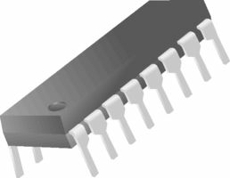
Vishay Siliconix SI9120DJ Current Mode PWM Controller 125mA 16-Pin PDIP Si9120 Series 13.5 V 0.15 mA Universal Input Switchmode Controller – SOIC-16
FEATURES
to 450-V Input Range· Current-Mode Control· 125-mA Output Drive· Internal Start-Up Circuit· Internal Oscillator (1 MHz)· SHUTDOWN and RESET
DESCRIPTION
The is a BiC/DMOS integrated circuit designed for use in low-power, high-efficiency off-line power supplies. High-voltage DMOS inputs allow the controller to work over a wide range of input voltages to 450-VDC). Current-mode PWM control circuitry is implemented in CMOS to reduce quiescent current to less than 1.5 mA. A CMOS output driver provides high-speed switching for MOSFET devices with gate charge, Qg, to 25 nC, enough to supply W of output power at 100 kHz. These devices, when combined with an output MOSFET and transformer, can be used to implement single-ended power converter topologies (i.e., flyback and forward). The Si9120 is available a 16-pin plastic DIP and SOIC packages, and is specified over the industrial, D suffix to 85°C) temperature range.
Applications information may also be obtained via FaxBack, request document #70580 and #70578.
Voltages Referenced to -VIN (Note: VCC < +VIN 0.3 V) VCC. 15 V +VIN. 450 V Logic Inputs (RESET SHUTDOWN, OSC IN, OSC OUT). V to VCC 0.3 V Linear Input (FEEDBACK, SENSE, BIAS, V HV Pre-Regulator Input Current (continuous).5 mAa Continuous Output Current (Source or Sink). 125 mA Storage Temperature. to 150°C Operating Temperature. to 85°C Junction Temperature (TJ). 150°C Power Dissipation (Package)b 16-Pin Plastic DIP (J Suffix)c. mW 16-Pin SOIC (Y Suffix)d. 900 mW Thermal Impedance (JA) 16-Pin Plastic 16-Pin SOIC.140°C/W Notes a. Continuous current may be limited by the applications maximum input voltage and the package power dissipation. b. Device mounted with all leads soldered or welded to PC board. c. Derate 6 mW/°C above 25°C. d. Derate 7.2 mW/°C above 25°C.
Voltages Referenced to -VIN 450 V fOSC. 40 kHz to 1 MHz ROSC. 1 M Linear Inputs. 0 to VCC 3 V Digital Inputs. 0 to VCC
Test Conditions Unless Specified Parameter Reference
Output Voltage Output Impedancee Short Circuit Current Temperature Stabilitye VR ZOUT ISREF TREF VREF = -VIN OSC = – VIN (OSC Disabled) 10 M Room Full Room Full k µA mV/°C
Maximum Frequencye Initial Accuracy Voltage Stability Temperature Coefficient
Feedback Input Voltage Input BIAS Current Input OFFSET Voltage Open Loop Voltage Gaine Unity Gain Bandwidthe Dynamic Output Impedancee Output Current Power Supply Rejection VFB IFB VOS AVOL BW ZOUT IOUT PSRR FB Tied to COMP OSC = – VIN (OSC Disabled) OSC = – VIN, VFB 4 V OSC = – VIN OSC = – VIN OSC = – VIN Error Amp configured for 60 dB gain Source VFB 3.4 V Sink VFB 9.5 V VCC 13.5 V Room mV dB MHz mA dB
Test Conditions Unless Specified Parameter Current Limit
Threshold Voltage Delay to Outpute VSOURCE td VFB 0 V VSENSE 1.5 V, See Figure 1. IIN 10 µA VCC 9.4 V IPRE-REGULATOR 10 µA Room V ns
Input Voltagef Input Leakage Current VCC Pre-Regulator Turn-Off Threshold Voltage Undervoltage Lockout VREG -VUVLO +VIN +IIN VREG VUVLO VDELTA Room V µA
Supply Current Bias Current ICC IBIAS pF at Pin 5 Room mA µA
SHUTDOWN Delaye SHUTDOWN Pulse Widthe RESET Pulse Widthe Latching Pulse Width SHUTDOWN and RESET Lowe Input Low Voltage Input High Voltage Input Current Input Voltage High Input Current Input Voltage Low tSD tSW tRW tLW VIL VIH IIH IIL VIN 10 V VIN 0 V See Figure 3. Room = 500 pF, VSENSE = -VIN See Figure 2. Room 50 100
Output High Voltage Output Low Voltage Output Resistance Rise Timee Fall Time Notes a. Refer to PROCESS OPTION FLOWCHART for additional information. b. Room = 25°C, Cold and Hot = as determined by the operating temperature suffix. c. The algebraic convention whereby the most negative value is a minimum and the most positive a maximum, is used in this data sheet. d. Typical values are for DESIGN AID ONLY, not guaranteed nor subject to production testing. e. Guaranteed by design, not subject to production test. f. 250V +VIN 380V place ¼ W resistor in series with +VIN (Pin 1). 380V +VIN 450V place ¼ W resistor in series with +VIN (Pin 1). Connect 0.01 µd capacitor between +VIN (Pin 1) and -VIN (Pin 6).
Manufacturer:Siliconix
Datasheet:Vishay/si9120.pdf


