Description
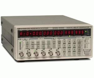
DG645/1 SRS Stanford Research Systems Pulse Generators 30.0V 10.00MHz Option 01 Eight delay channels (5V)
Stanford Research Systems DG645 Overview
The DG645 is a versatile digital delay/pulse generator that provides precisely defined pulses at repetition rates up to 10 MHz. The instrument offers several improvements over older designs lower jitter, higher accuracy, faster trigger rates, and more outputs. The DG645 also has Ethernet, GPIB and RS-232 interfaces for computer or network control of the instrument.
All digital delay generators measure time intervals by counting cycles of a fast clock (typically 100 MHz). Most digital delay generators also have short programmable analog delays to achieve time intervals with finer resolution than the clock period. Unfortunately, one clock cycle of timing indeterminacy (typically 10 ns) can occur if the trigger is not in phase with the clock.
The DG645 eliminates timing indeterminacy by measuring the timing of triggers with respect to the internal clock and compensating the analog delays. This approach reduces the jitter by about 100 and allows the internal rate generator to operate at any rate not just a sub-multiple of the clock frequency.
The DG645 has many trigger modes. An internal rate generator, with less than 100 ps period jitter, may be set from 100 Hz to 10 MHz with 1 Hz resolution. An external trigger input, with adjustable threshold and slope, can trigger a timing cycle, a burst of cycles, or a single shot. A single shot can be triggered with a key press. A line trigger operates synchronously with the AC mains. A rear-panel trigger inhibit input can disable the trigger or any of the pulse outputs during a timing cycle.
Specifications
| Channels | 4 independent pulses controlled in position and width. 8 delay channels available as an option (see Output Options). |
| Range | 0 to 2000 s |
| Resolution | 5 ps |
| Accuracy | 1 ns + (timebase error × delay) |
| Jitter (rms) | |
| Ext. trig. to any output | |
| T0 to any output | |
| Trigger delay | 85 ns (ext. trig. to T0 output) |
| Timebase | Std, crystal, 10–8, 2 × 10⁻⁶, 5 |
| Opt. 4, OCXO, 10–11, 1 × 10⁻⁹, 0.2 | |
| Opt. 5, Rb, 10–11, 1 × 10⁻¹⁰, 0.0005 | |
| External input | 10 MHz ± 10 ppm, sine >0.5 Vpp, 1 kΩ impedance |
| Output | 10 MHz, 2 Vpp sine into 50 Ω |
| External Trigger | |
| Rate | DC to 1/(100 ns + longest delay)(maximum of 10 MHz) |
| Threshold | ±3.50 VDC |
| Slope | Trigger on rising or falling edge |
| Impedance | 1 MΩ + 15 pF |
| Internal Rate Generator | |
| Trigger modes | Continuous, line or single shot |
| Rate | 100 µHz to 10 MHz |
| Resolution | 1 µHz |
| Accuracy | Same as timebase |
| Jitter (rms) | |
| Burst Generator | |
| Trigger to first T&sub0; | |
| Range | 0 to 2000 s |
| Resolution | 5 ps |
| Period between pulses | |
| Range | 100 ns to 42.9 s |
| Resolution | 10 ns |
| Delay cycles per burst | 1 to 2³² – 1 |
| Resolution | 5 ps |
| Outputs (T0, AB, CD, EF and GH) | |
| Source impedance | 50 Ω |
| Transition time | |
| Overshoot | |
| Offset | ±2 V |
| Amplitude | 0.5 to 5.0 V (level + offset <6.0 v=”” td=””> |
| Accuracy | 100 mV + 5 % of pulse amplitude |
| General | |
| Computer interfaces | GPIB (IEEE-488.2), RS-232 and Ethernet. All instrument functions can be controlled through the interfaces. |
| Non-volatile memory | Nine sets of instrument configurations can be stored and recalled. |
| Power | |
| Dimensions | 8.5″ × 3.5″ × 13″ (WHL) |
| Weight | 9 lbs. |
| Warranty | One year parts and labor on defects in materials & workmanship |
| Output Options | |
| Option 1 (8 Delay Outputs on Rear Panel) | |
| Outputs (BNC) | T0, A, B, C, D, E, F, G and H |
| Source impedance | 50 Ω |
| Transition time | |
| Overshoot | |
| Level | +5 V CMOS logic |
| Pulse characteristics | |
| Rising edge | At programmed delay |
| Falling edge | 25 ns after longest delay |
| Option 2 (8 High-Voltage Delay Outputs on Rear Panel) | |
| Outputs (BNC) | T0, A, B, C, D, E, F, G and H |
| Source impedance | 50 Ω |
| Transition time | |
| Levels | 0 to 30 V into high impedance, 0 to 15 V into 50 Ω (amplitude decreases by 1 %/kHz) |
| Pulse characteristics | |
| Rising edge | At programmed delay |
| Falling edge | 100 ns after the rising edge |
| Option 3 (Combinatorial Outputs on Rear Panel) | |
| Outputs (BNC) | T0, AB, CD, EF, GH, (AB+CD), (EF+GH), (AB+CD+EF), (AB+CD+EF+GH) |
| Source impedance | 50 Ω |
| Transition time | |
| Overshoot | |
| Pulse characteristics | |
| T0, AB, CD, EF, GH | Logic high for time between delays |
| (AB+CD), (EF+GH) | Two pulses created by the logic OR of the given channels |
| (AB+CD+EF) | Three pulses created by the logic OR of the given channels |
| (AB+CD+EF+GH) | Four pulses created by the logic OR of the given channels |
| Option SRD1 (Fast Rise Time Module) | |
| Rise time | |
| Fall time | |
| Offset | -0.8 V to -1.1 V |
| Amplitude | 0.5 V to 5.0 V |
| Load | 50 Ω |
Manufacturer:Electronic Components
Datasheet:DG645c.pdf


